Advances in Solid State Part 2 pdf
Bạn đang xem bản rút gọn của tài liệu. Xem và tải ngay bản đầy đủ của tài liệu tại đây (631.9 KB, 30 trang )
CMOS Nonlinear Signal Processing Circuits
21
shows the rank-order function, whereas Fig. 22(b) shows the function of the k-WTA. On the
average, the accuracy of whole circuit was approximated 150 mV. The performance of the
chip was degraded by many factors such as the mismatch in comparator cells, the different
capacitance at input terminals of the evaluation cells, and the clock feed-through error. Due
to these non-ideal effects, each rank-order function was finished in 20 μs. After increasing
supply voltage up to 1.5 V and proper biasing voltage V
bias
adjusting, the performance of the
circuit can be improved. Including power consumption of the input/output pads, the static
power consumption of the chip was 1.4 mW.
Many factors such as precision, speed, process variation, and chip area must be considered
for design of a low-power low-voltage rank order extractor.
1.
Limitations of low voltage and low power
The average power consumption of the circuit is expressed by
currentshort
static
dynamic
PPPP
_
+
+
=
DDscDD
leakage
oDD
VfQVIIVCf +++= )(
2
(11)
where f is the frequency, C is the capacitance in the circuit, V
DD
is the voltage supply, I
o
is the
standby current, I
leakage
is the leakage current, and the Q
sc
is the short-current charge during
the clock transient period. In order to reduce the power consumption, the voltage supply
V
DD
must be reduced, and the standby current in the comparator and evaluation cell must
be designed as small as possible. In mask layout, the clock and its complementary are
generated locally to reduce delay and mismatch. Thus, the probability of a short current
occurring in the circuit is minimized.
2.
Speed and precision
The accuracy of the comparators determines the resolution of the circuit. For the comparator
design, the smallest differential voltage, that is, distinguished correctly is influenced by two
factors. One is the charge-injection error in analog switches, and the other is the parasitic
capacitor C
p
effect. The effect is reduced by enlarging the sampling capacitor C
s
and making
the switches dimension as small as possible. In the design, the response time
τ
of the
extractor is the summation of the auto-zero time
az
τ
, the comparison time
cmp
τ
, and the
evaluation time
eval
τ
.
eval
cmpaz
τ
τ
τ
τ
+
+
=
(12)
Reducing
az
τ
,
cmp
τ
and
eval
τ
will improve the response time
τ
. The minimum auto-zero
time
az
τ
is required to sample the input voltage correctly at sampling capacitor C
s
and to
bias the inverter properly at high gain region. The switches shown in Fig. 19 with larger
dimension reduce auto-zero time
az
τ
. However, the clock feed-through error and charge
injection error will also be enlarged during the clock transition. In the same situation, the
smaller sample capacitor C
s
will reduce the time
az
τ
. Unfortunately, it will reduce the
effective magnitude of the difference voltage; thus, the comparator accuracy is degraded.
The comparison time
cmp
τ
dominates the response time
τ
, especially when the input levels
are close each other. Since the amplification in the transition region of a CMOS inverter
operated at low voltage supply is not high enough, the comparator must take a long time to
Advances in Solid State Circuits Technologies
22
identify which input variable has a larger level. The evaluation time
eval
τ
is defined so that
the time interval between the comparator cells generates the proper currents and the
extractor has finished finding the desired rank order. Time
eval
τ
is a function of the current
I
unit
. The maximum number M of input variables is also influenced by the current I
unit
.
Although reducing the magnitude of the current I
unit
is able to reduce the power
consumption, however, the relationship among
eval
τ
, I
unit
, and M in this architecture is a
complicated function.
3.
Process variation analysis
With contemporary technology, process variation during fabrication cannot be completely
eliminated; as a result, mismatch error must be noticed in VLSI circuit design. The match in
dimension of the binary-weight MOS in the evaluation cell (M1 - M8 in Fig. 20) is an
important factor for the circuit operation. If the mismatch error induces an error current I
err
larger (or smaller) than half of the unit current I
unit
, decision of the evaluation cell fails. Thus,
a rough estimated constraint for I
err
is
2/
uniterr
II
<
. (13)
5. Conclusion
The chapter describes various nonlinear signal processing CMOS circuits, including a high
reliable WTA/LTA, simple MED cell, and low-voltage arbitrary order extractor. We focus
the discussion on CMOS analog circuit design with reliable, programmable capability, and
low voltage operation. It is a practical problem when the multiple identical cells are required
to match and realized within a single chip using a conventional process. Thus, the design of
high-reliable circuit is indeed needed. The low-voltage operation is also an important design
issue when the CMOS process scale-down further. In the chapter, Section 1 introduces
various CMOS nonlinear function and related applications. Section 2 describes design of
highly reliable WTA/LTA circuit by using single analog comparator. The analog
comparator itself has auto-zero characteristic to improve the overall reliability. Section 3
describes a simple analog MED cell. Section 4 presents a low-voltage rank order extractor
with k-WTA function. The flexible and programmable functions are useful features when
the nonlinear circuit will integrate with other systems. Depend on various application
requirements, we must have different design strategies for design of these nonlinear signal
process circuits to achieve the optimum performance. In state-of-the-art process, small chip
area, low-voltage operation, low-power consumption, high reliable concern, and
programmable capability still have been important factors for these circuit realizations.
6. References
Aksin, D. Y. (2002). A high-precision high-resolution WTA-MAX circuit of O(N) complexity.
IEEE Trans. Circuits Syst. II, Analog Digit. Signal Process., vol. 49, no. 1, 2002, pp. 48–
53.
Cilingiroglu, U. & Dake, L. E. (2002). Rank-order filter design with a sampled-analog
multiple-winners-take-all core. IEEE J. Solid-State Circuits, vol. 37, Aug. 2002, pp.
978 – 984.
CMOS Nonlinear Signal Processing Circuits
23
Demosthenous, A.; Smedley, S. & Taylor, J. (1998). A CMOS analog winner-take-all network
for large-scale applications. IEEE Trans. Circuits Syst. I, Fundam. Theory Appl., vol.
45, no. 3, 1998, pp. 300–304.
Diaz-Sanchez, A.; Jaime Ramirez-Angulo; Lopez-Martin, A. & Sanchez-Sinencio, E. (2004). A
fully parallel CMOS analog median filter. IEEE Trans. Circuits Syst. II, vol. 51,
March 2004, pp. 116 – 123.
He, Y. & Sanchez-Sinencio, E. (1993). Min-net winner-take-all CMOS implementation.
Electron. Lett., vol. 29, no. 14, 1993, pp. 1237–1239.
Hosotani, S.; Miki, T.; Maeda, A. & Yazawa, N. (1990). An 8-bit 20-MS/s CMOS A/D
converter with 50-mW power consumption. IEEE J. Solid-State Circuits, vol. 25, no.
1, Feb. 1990, pp. 167-172.
Hung, Y C. & Liu, B D. (2002). A 1.2-V rail-to-rail analog CMOS rank-order filter with k-
WTA capability. Analog Integr. Circuits Signal Process., vol. 32, no. 3, Sept. 2002, pp.
219-230.
Hung, Y C. & Liu, B D. (2004). A high-reliability programmable CMOS WTA/LTA circuit
of O(N) complexity using a single comparator. IEE Proc.—Circuits Devices and Syst.,
vol. 151, Dec. 2004, pp. 579-586.
Hung, Y C.; Shieh, S H. & Tung, C K. (2007). A real-time current-mode CMOS analog
median filtering cell for system-on-chip applications. Proceedings of IEEE Conference
on Electron Devices and Solid-State Circuits (EDSSC), pp. 361 – 364, Dec. 2007, Tainan,
Taiwan.
Lazzaro, J.; Ryckebusch, R.; Mahowald, M. A. & Mead, C. A. (1989). Winner-take-all
networks of O(N) complexity. Advances in Neural Inform. Processing Syst., vol. 1,
1989, pp. 703-711.
Lippmann, R. (1987). An introduction to computing with neural nets. IEEE Acoust., Speech,
Signal Processing Mag., vol. 4, no. 2, Apr. 1987, pp. 4-22.
Opris, I. E. & Kovacs, G. T. A. (1994). Analogue median circuit. Electron. Lett., vol. 30, no. 17,
Aug. 1994, pp. 1369-1370.
Opris, I. E. & Kovacs, G. T. A. (1997). A high-speed median circuit. IEEE J. Solid-State
Circuits, vol. 32, June 1997, pp. 905-908.
Semiconductor Industry Association. (2008). International technology roadmap for
semiconductors 2008 update. [Online]. Available:
Smedley, S.; Taylor, J. & Wilby, M. (1995). A scalable high-speed current mode winner-take-
all network for VLSI neural applications. IEEE Trans. Circuits Syst. I, Fundam. Theory
Appl., vol. 42, no. 5, 1995, pp. 289–291.
Starzyk, J.A. & Fang, X. (1993). CMOS current mode winner-take-all circuit with
both excitatory and inhibitory feedback. Electron. Lett., vol. 29, no. 10, 1993, pp. 908–
910.
Vlassis, S. & Siskos, S. (1999). CMOS analogue median circuit.
Electron. Lett., vol. 35, no. 13,
June 1999, pp. 1038-1040.
Yamakawa, T. (1993). A fuzzy inference engine in nonlinear analog mode and its
applications to a fuzzy logic control. IEEE Trans. Neural Netw., vol. 4, no. 3, May
1993, pp. 496–522.
Advances in Solid State Circuits Technologies
24
Yuan, J. & Stensson, C. (1989). High - speed CMOS circuit technique. IEEE J. Solid-State
Circuits, vol. 24, no. 1, Feb. 1989, pp. 62-69.
2
Transconductor
Ko-Chi Kuo
Department of Computer Science and Engineering,
National Sun Yat-sen University Kaohsiung,
Taiwan
1. Introduction
The transconductor is a versatile building block employed in many analog and mixed-signal
circuit applications, such as continuous-time filters, delta-sigma modulators, variable gain-
amplifier or data converter. The transconductor is to perform voltage-to-current conversion.
Linearity is one of most critical requirements in designing transconductor. Especially in
designing delta-sigma modulators for high resolution Analog/Digital converters, it needs
high linearity transconductors to accomplish the required signal-to-(noise+distortions) ratio.
The tuning ability of transconductor is also mandated to adjust center frequency and quality
factor in filter applications.
The portable electronic equipments are the trend in comsumer markets. Therefore, the low
power consumption and low supply voltage becomes the major challenge in designing
CMOS VLSI circuitry. However, designing for low-voltage and highly linear
transconductor, it requires to consider many factors. The first factor is the linear input range.
The range of linear input is justified by the constant transconductance, G
m
. Since the
distortion of transconductor is determined by the ratio of output currents versus input
voltage. The second factor is the control voltage of transconductor. This voltage can greatly
impact the value of transconductance, linear range, and power consumption. For example,
when the control voltage increases, the transconductance also increase but the linear input
range of transconductor is reduced and power consumption is increased. Hence it is critical
in designing transconducotr operated at low supply voltage. The third factor is the
symmetry of the two differential outputs. If the transconductance of the positive and
negative output is G
m+
=I
O+
/V
i
and G
m−
=I
O−
/V
i
, then how close G
m+
and G
m−
should be is a
critical issue, where I
O+
is the positive output current, I
O−
is the negative output current, and
V
i
is the input differential voltage. This factor is the major cause of common-mode distortion
of transconductor which occurs at outputs.
In general, the design of differential transconductor can be classified into triode-mode and
saturation-mode methods depending on operation regions of input transistors. Triode-mode
transconductor has a better linearity as well as single-ended performance. On the other
hand, saturation-mode transconductor has better speed performance. However, it only
exhibits moderate linearity performance. Furthermore, the single-ended transconductor of
saturation-mode suffers from significant degradation of linearity. Several circuit design
techniques for improving the linearity of transconductors have been reported in literatures.
The linearization methods include: source degeneration using resistors or MOS transistors
Advances in Solid State Circuits Technologies
26
[Krummenacher & Joeh, 1988; Leuciuc & Zhang, 2002; Leuciuc, 2003; Furth & Andreou,
1995], crossing-coupling of multiple differential pairs [Nedungadi & Viswanathan, 1984;
Seevinck & Wassenaar, 1987] class-AB configuration [Laguna et al., 2004; Elwan et al., 2000;
Galan et al., 2002], adaptive biasing [Degrauwe et al., 1982; Ismail & Soliman, 2000;
Sengupta, 2005], constant drain-source voltages [Kim et al., 2004; Fayed & Ismail, 2005;
Mahattanakul & Toumazou, 1998; Zeki, 1999; Torralba et al., 2002; Lee et al., 1994;
Likittanapong et al., 1998], pseudo differential stages [Gharbiya & Syrzycki, 2002], and shift
level biasing [Wang & Guggenbuhl, 1990].
Source degeneration using resistors or MOS transistors is the simplest method to linearize
transconductor. However, it requires a large resistor to achieve a wide linear input range. In
addition, MOS used as resistor exhibits considerable varitions affected by process and
temperture and results in the linearity degradation. Crossing-coupling with multiple
differential pairs is designed only for the balanced input signals. The Class-AB configuration
can achieve low power consumption. On the other hand, the linearity is the worst due to the
inherited Class-AB structure. The adaptive biasing method generates a tail current which is
proportional to the square of input differential voltage to compensate the distortion caused
by input devices. However, the complication of square circuitry makes this technique hard
to implement. The constant drain-source voltage of input devices is a simple structure. It can
achieve a better linearity with tuning ability. However, it needs to maintain V
DS
of input
devices in low voltage and triode region. Therefore, this technique is difficult to implement
in low supply voltage. Hence, a new transconductor using constant drain-source voltage in
low voltage application is proposed to achieve low-voltage, highly linear, and large tuning
range abilities.
In section 2, basic operatrion and disadvantage of the linerization techniques are described.
The proposed new transconductor is presented in section 3. The simulation results and
conclusion are given in section 4 and 5.
2. Linearization techniques
In this section, reviews of common linearization techniques reported in literatures are
presented. The first one is the transconductor using constant drain-source voltage. The
second one is using regulated cascode to replace the auxiliary amplifier. The third one is
transconductor with source degeneration by using resistors and MOS transistors. The last
one is the linear MOS transconductor with a adaptive biasing scheme. Besides introducing
their theories and analyses, the advantages and disadvantages of these linearization
techniques are also discussed.
2.1 Transconductor using constant drain-source voltage
The idea of transconductors using constant drain-source voltages is to keep the input
devices in triode region such that the output current is linearized. The schematic of this
method is shown in Fig. 1. Considering that transistors M
1
, M
2
operate at triode region, M
3
,
M
4
are biased at saturation region, channel length modulation, body effect, and other
second-order effects are ignored, the drain current of M
1
and M
2
is given by
()
⎥
⎦
⎤
⎢
⎣
⎡
−−=
2
2
DS
DSTGSD
V
VVVI
β
(1)
Transconductor
27
where
β
=
μ
n
C
OX
(W/L), V
GS
is the gate-to-source voltage, V
T
is the threshold voltage, and V
DS
is the drain-to-source voltage. If the two amplifiers in Fig. 1 are ideal amplifiers, then
CDSDS
VVV
=
=
21
(2)
Fig. 1. Transconductor using constant drain-source voltage
The transfer characteristic of this transconductor is given by
() ()
⎥
⎦
⎤
⎢
⎣
⎡
−−=
⎥
⎦
⎤
⎢
⎣
⎡
−−=
22
2
1
2
1
111
C
CTGS
DS
DSTGSout
V
VVV
V
VVVI
ββ
() ()
⎥
⎦
⎤
⎢
⎣
⎡
−−=
⎥
⎦
⎤
⎢
⎣
⎡
−−=
22
2
2
2
2
222
C
CTGS
DS
DSTGSout
V
VVV
V
VVVI
ββ
(
)
2121 ininCoutoutout
VVVIII
−
=
−
=
β
(3)
The transconductance value is
Cm
VG
β
=
(4)
In fact, it is difficult to design an ideal amplifier implemented in this circuits. However, it
can force
V
DS1
=V
DS2
=V
DS
by using two auxiliary amplifiers controlled with the same V
C
to
keep V
DS
at the constant value. Therefore, the transfer characteristic of this transconductor is
changed as follows:
() ()
⎥
⎦
⎤
⎢
⎣
⎡
−−=
⎥
⎦
⎤
⎢
⎣
⎡
−−=
22
2
1
2
1
111
DS
DSTGS
DS
DSTGSout
V
VVV
V
VVVI
ββ
() ()
⎥
⎦
⎤
⎢
⎣
⎡
−−=
⎥
⎦
⎤
⎢
⎣
⎡
−−=
22
2
2
2
2
222
DS
DSTGS
DS
DSTGSout
V
VVV
V
VVVI
ββ
Advances in Solid State Circuits Technologies
28
(
)
2121 ininDSoutoutout
VVVIII
−
=
−
=
β
(5)
, where V
GS1
= V
in1
and V
GS2
= V
in2
.
Therefore, the new transconductance value is
DSm
VG
β
=
(6)
The linearity of this transconductor is moderated. It is also easy to implement in circuit.
However,
V
DS
of the input devices must be small enough to keep transistors in triode region.
The following condition has to be satisfied:
TGSDS
VVV −<
(7)
On the other hand, the auxiliary amplifiers need to design carefully to reduce the overhead
of extra area and power.
2.2 Transconductor using regulated cascode to replace auxiliary amplifier
In Fig. 2(a) regulating amplifier keeps
V
DS
of M
1
at a constant value determined by V
C
. It is
less than the overdrive voltage of M
1
. The voltage can be controlled from V
C
so as to place
M
3
in current-voltage feedback, thereby increasing output impedance. The concept is to
drive the gate of M
3
by an amplifier that forces V
DS1
to be equal to V
C
. Therefore, the voltage
variations at the drain of M
3
affect V
DS1
to a lesser extent because amplifiers “regulate” this
voltage. With the smaller variations at V
DS1
, the current through M
1
and hence output
current remains more constant, yielding a higher output impedance [Razavi, 2001]
133 OOmout
rrAgR ≈
(8)
(a) (b)
Fig. 2. (a)Basic triode transconductor structure (b) Simple RGC triode transconductor
Transconductor
29
It is one of solutions using regulated cascode to replace the auxiliary amplifier in order to
overcome restrictions on Fig. 1. The circuit in Fig. 2(b) proposed in [Mahattanakul &
Toumazou, 1998] uses a single transistor, M
5
, to replace the amplifier in Fig. 2(a). This circuit
called regulated cascode which is abbreviated to RGC. The RGC uses M
5
to achieve the gain
boosting by increasing the output impedance without adding more cascode devices.
V
DS1
is
calculated by follows: Assuming M
5
is in saturation region in Fig. 2(b). It can be shown that
()
2
55
2
1
TGSC
VVI −=
β
=>
5
5
15
2
T
C
CDSGS
V
I
VVV +=−=
β
=>
5
5
1
2
T
C
CDS
V
I
VV ++=
β
(9)
From (6)
⎟
⎟
⎠
⎞
⎜
⎜
⎝
⎛
++==
5
5
111
2
T
C
CDSm
V
I
VVG
β
ββ
. Thus, G
m
can be tuned by using a controllable
voltage source V
C
or current source I
C
. However, it is preferable in practice to use a
controllable voltage source
V
C
for lowering power consumption since V
DS1
only varies as a
square root function of I
C
.
Simple RGC transconductor using a single transistor to achieve gain boosting can reduce
area and power wasted by the auxiliary
amplifiers. However, it still has some
disadvantages. First, it will cause an excessively high supply-voltage requirement and also
produce an additional parasitic pole at the source of transistors. Therefore, it can not apply
to the low-supply voltage design. Second, the tuning range of
V
DS1
is restricted. The smallest
value of
V
DS1
is
T
C
V
I
+
5
2
β
when V
C
= 0. In other words, V
DS1
can not be set to zero. Owing
to the restriction of (7),
V
DS
is as low as possible and the best value is zero. Third, V
T
dependent
G
m
may be a disadvantage due to the substrate noise and V
T
mismatch problems
[Lee et al., 1994].
In Fig. 3, another RGC transconductor that can apply to the low-voltages applications is
proposed in [Likittanapong et al., 1998]. The circuit overcomes the disadvantages mentioned
above is to utilize PMOS transistor that can operate in saturation region as gain boosting.
The use of this PMOS gain boosting in the feedback path can result in a circuit with a wide
transconductance tuning range even at the low supply voltage. In [Likittanapong et al.,
1998], it mentions that at the maximum input voltage, M
3
may be forced to enter triode
region, especially if the dimension of M
2
is not properly selected, resulting in a lower
dynamic range. Besides, β
2
may be chosen to be larger for a very low distortion
transconductor. It means that the tradeoff between linearity and bandwidth of
transconductor is controlled by
β
2
. Therefore, β
2
should be selected to compromise these two
characteristics for a given application.
V
DS1
is calculated by follows. Assuming M
3
is in saturation region in Fig. 3.
Advances in Solid State Circuits Technologies
30
()
2
333
2
1
TGSC
VVI −=
β
=>
3
3
13
2
T
C
DSCGS
V
I
VVV +=−=
β
=>
⎟
⎟
⎠
⎞
⎜
⎜
⎝
⎛
+−=
3
3
1
2
T
C
CDS
V
I
VV
β
(10)
From (6)
⎥
⎥
⎦
⎤
⎢
⎢
⎣
⎡
⎟
⎟
⎠
⎞
⎜
⎜
⎝
⎛
+−==
3
3
111
2
T
C
CDSm
V
I
VVG
β
ββ
. It shows that V
DS1
can be set to zero when
3
3
2
T
C
C
V
I
V +=
β
. Therefore, this transconductor has a wider tuning range compared to that of
RGC transconductor and is capable of working in low-supply voltage (3V). However, this
transconductor still has some drawbacks. The major drawback is the tuning ability. For
example, it is difficult to control
3
3
2
T
C
C
V
I
V +=
β
if V
DS1
is set to zero. The minor drawback
is that V
T
depends on the G
m
. It also may cause substrate noise and V
T
mismatch problems
[Lee et al., 1994].
I
C
V
in
V
C
I
out
M
1
M
2
M
3
Fig. 3. RGC transconductor with PMOS gain stage
2.3 Transconductor using source degeneration
A simple differential transconductor is shown in Fig. 4(a). Assuming that M
1
and M
2
are in
saturation and perfectly matched, the drain current is given by
()
2
2
TGSD
VVI −=
β
(11)
Transconductor
31
The transfer characteristic using (5) is given by
()
TGS
i
iSS
SS
i
iSSoutoutout
VV
V
VI
I
V
VIIII
−
−=−=−=
4
12
8
12
22
21
β
β
β
(12)
, where V
i
= (V
in1
−V
in2
)
If V
GS
is large enough, the higher linearity can be achieved. Unfortunately, it can not be used
in the low-voltage application and the linear input range is limited. Simplest techniques to
linearize the transfer characteristic of MOS transconductor is the one with source
degeneration using resistors as shows in Fig. 4(b). The circuit is described by
21 GSGSouti
VVRIV −=−
(13)
A transfer characteristic derived from (13) is given by
()
()
SS
outi
outiSSout
I
RIV
RIVII
8
12
2
−
−−=
β
β
(14)
The transconductance G
m
is
Rg
g
G
m
m
m
+
≈
1
(15)
where g
m
is the transconductance of transistor M
1
and M
2
.
We should notice that in (14), the nonlinear term depends on V
i
− RI
out
rather than V
i
. Higher
linearity can be achieved when R >> 1/g
m
. The disadvantage of this transconductor is that
large resistor value is needed in order to maintain a wider linear input range. Owing to
G
m
≈ 1/R, the higher transconductance is limited by the smaller resistor. Hence, there is a
tradeoff between wide linear input range and higher transconductance which is mainly
determined by a resistor.
1in
V
2in
V
SS
I
2out
I
1out
I
SS
I
1out
I
2out
I
1in
V
2in
V
SS
I2
1
M
1
M
2
M
2
M
(a) (b)
Fig. 4. (a) Simple differential MOS transconductor (b) MOS transconductor with resistive
source degeneration
Advances in Solid State Circuits Technologies
32
Another method to linearize the transfer characteristic of MOS transconductor is using source
degeneration to replace the degeneration resistor with two MOS transistors operating in triode
region. The circuit is shown in Fig. 5. Notice that the gates of transistor M
3
and M
4
connect to
the differential input voltage rather than to a bias voltage. To see that M
3
and M
4
are generally
in triode region, we look at the case of the equal input signals (V
in1
=V
in2
), resulting in
11 GSinyx
VVVV
−
=
=
(16)
Therefore, the drain-source voltages of M
3
and M
4
are zero. However, V
DS
of M
3
and M
4
equal those of M
1
and M
2
. Owing to (7), M
3
and M
4
are indeed in triode region. Assuming
M
3
, M
4
are operating in triode region, the small-signal drain-source resistance of M
3
, M
4
is
given by
()
TGS
dsds
VV
rr
−
==
13
43
1
β
(17)
It must be noted that in this circuit the effect of varying V
DS
of M
1
and M
2
can not be ignored
since the drain currents are not fixed to a constant value. The small-signal source resistance
of M
1
, M
2
is given by
()
1111
21
11
TGSm
ss
VVg
rr
−
===
β
(18)
Using small-signal T model, the small-signal output current, i
o1
, is
equal to
()
4321
21
1
||
dsdsss
inin
o
rrrr
VV
i
++
−
=
=>
()()
2111
31
31
1
4
2
ininTGSo
VVVVi −−
+
=
ββ
ββ
(19)
Assuming M
1
is in saturation region, the drain current of M
1
is given by
()
2
111
2
1
TGSSS
VVI −=
β
=>
()
1
11
2
β
SS
TGS
I
VV =−
(20)
Using (20) substitutes for (19), that leads to
()
21
131
31
1
2
4
2
inin
SS
o
VV
I
i −
+
=
βββ
ββ
(21)
The transconductance G
m
is
131
31
2
4
2
βββ
ββ
SS
m
I
G
+
= (22)
Transconductor
33
Linearity can be enhanced (assuming r
ds3
>> r
s1
) compared to that of a simple differential
pair because transistors operated in triode region exhibits higher linearity than the source
resistances of transistors operated in saturation region. When the input signal is increased,
the small-signal resistance in one of two triode transistors in parallel, M
3
or M
4
, is reduced.
Meanwhile, the reduced resistance results in the lower linearity and the larger
transconductance. As discussed in [Krummenacher & Joeh, 1988], if the proper size ratio of
β
1
/
β
3
is chosen, the balance between higher linearity and stable transconductance can be
achieved. How to choose the optimum size ratio of
β
1
/
β
3
for the best linearity performance
becomes slightly dependent on the quiescent overdrive voltage, V
GS
−V
T
. The size ratio of
β
1
/
β
3
=6.7 is used to achieve the best linearity performance.
According to (22), the transconductance can be tuned by changing I
SS
and size ratio of
β
1
/
β
3
.
Nevertheless, the nonlinearity error is up to 1% for I
out
/I
SS
< 80%. It is required to have a
better linearity so as to achieve a THD of -60 dB or less in some filtering applications [Kuo &
Leuciuc, 2001].
1in
V
1
M
2
M
3
M
4
M
SS
I
SS
I
1out
I
2out
I
2
in
V
Fig. 5. Transconductor with source degeneration using MOS transistors
2.4 Transconductor using adaptive biasing
The transconductor using adaptive biasing is shown in Fig. 6. All transistors are assumed to
be operated in saturation region, neglecting channel lengh modulation effect. First,
transistor M
3
is absent, and output current as a function of two input voltages V
in1
and V
in2
is
obtained as
()
2
11
2
TGS
VVI −=
β
()
2
22
2
TGS
VVI −=
β
=>
()
(
)
SS
inin
ininSSout
I
VV
VVIIII
4
1
2
21
2121
−
−−=−=
β
β
(23)
Advances in Solid State Circuits Technologies
34
, where I
SS
is a tail current and equals I
B
.
An adaptive biasing technique is using a tail current containing an input dependent
quadratic component to cancel the nonlinear term in (23). Consequently, the circuit in Fig. 6
changes the tail current by adding transistor M
3
. The tail current will be changed by
CBSS
III +=
(24)
()
2
21
4
ininC
VVI −=
β
(25)
, where I
B
is tail current of differential pair and I
C
is the compensating tail current that cancel
nonlinear term.
Therefore, the transfer characteristic is changed by
(
)
21 ininSSout
VVII −=
β
(26)
1
M
2
M
3
M
4
M
5
M
6
M
1in
V
2
in
V
C
V
B
V
out
I
VDD
C
I
B
I
Fig. 6. Transconductor with adaptive biasing
3. New transconductor
The conventional structure which uses the constant drain source-voltage such as RGC with
NMOS or PMOS can not operate at 1.8V or below. The main reason is that auxiliary amplifier
under the low supply voltage can’t provide enough gain to keep the constant drain-source
voltage. Therefore, we propose a triode transconductor which uses new structure to replace
the auxiliary amplifier. Fig. 7 shows the proposed triode transconductor structure.
MOS M
5
, M
7
, M
9
and M
11
are made up a two-stage amplifier to replace the auxiliary
amplifier. The two-stage amplifier is implemented using M
9
with the active loads M
11
formed the first stage and M
5
with the active load M
7
formed the second stage. The first and
second stages exhibit gains equal to
(
)
11
1
991
||
Om
rggmA
−
= (27)
(
)
7552
||
OO
rrgmA =
(28)
Transconductor
35
1
M
3
M
5
M
7
M
1in
V
9
M
11
M
C
V
1out
I
1Bias
V
2Bias
V
13
M
Fig. 7. Proposed triode transconductor
Therefore, the overall gain is
(
)
(
)
75511
1
9921
||||*
OOOmv
rrgmrggmAAA
−
== (29)
The proposed transconductor is shown in Fig. 8.
C
V
2
M
8
M
12
M
C
V
1in
V
1
M
2in
V
3
M
4
M
7
M
5
M
9
M
6
M
10
M
11
M
2out
I
1out
I
Bias
V
13
M
14
M
15
M
16
M
Fig. 8. The proposed transconductor
Considering that the large gain is achieved and is able to keep transistors M
1
and M
2
in
triode region, the drain current of M
1
and M
2
is given by
()
⎥
⎦
⎤
⎢
⎣
⎡
−−=
2
2
1
11111
DS
DSTGSout
V
VVVI
β
(30)
()
⎥
⎦
⎤
⎢
⎣
⎡
−−=
2
2
2
22222
DS
DSTGSout
V
VVVI
β
(31)
The transfer characteristic is given by
Advances in Solid State Circuits Technologies
36
(
)
211121 ininDSoutoutout
VVVIII
−
=
−
=
β
(32)
, where
β
1
=
β
2
, V
T1
=V
T2
, and V
DS1
= V
DS2
. Assuming that current I
9
flows from M
11
through
M
9
and MOS M
9
is in saturation region, V
DS1
can be found in (33)
713 DSDSGS
VVV
=
+
77 DSTC
VVV =−
=>
713 TCDSGS
VVVV
−
=
+
371 GSTCDS
VVVV −−=
(33)
According to (32)
(
)
(
)
(
)
213712111 ininGSTCininDSout
VVVVVVVVI
−
−
−
=
−
=
β
β
(34)
The transconductance G
m
is
(
)
371 GSTCm
VVVG
−
−
=
β
(35)
From (35), the transconductance can be tuned by control voltage V
C
To keep M
1
and M
2
in
triode region, the relation (36) needs to be satisfied.
111 TGSDS
VVV −< (36)
Using (33) to substitute (36)
1137 TGSGSTC
VVVVV
−
≤
−
−
)(
7131 TTGSGSC
VVVVV
−
−
+
≤
=
> (37)
The proposed transconductor is suitable for low supply voltage and we choose 1.8V to
achieve a wide linear range. Moreover, M
9
is needed to obtain a negative feedback to keep
the drain-source voltage of M
1
, V
DS1
, constant. This new structure can provide enough gain
to keep V
DS1
constant at 1.8V supply voltage. It has a low control voltage V
C
between
0.69V~0.72V and the large transconductance tuning range depending on applications.
Besides, it has a simple structure so as to save area.
4. Simulation results
The circuits in Fig. 8 have been designed by using TSMC CMOS 0.18μm process with a
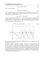
single 1.8V supply voltage and simulated by Hspice. Fig. 9. shows the curve of input voltage
transferring to the output current at V
C
= 0.7V. The slope of the curve is linear when the
input voltage varies from −1V to 1V. The slope in Fig. 9. is equal to the transconductance in
Fig. 10. In order to verify the performance of the proposed transconductor, we define
transconductance error (equation 39) as the linearity of the transconductance’s output
current. The transconductance error is less than 1% among ±0.9V input voltage, so the input
linear range is up to 1.8V.
(
)
(
)
()
100*
0
0
(%)
m
midm
G
GVG
TE
−
= (39)
Transconductor
37
Fig. 9. V-I transfer characteristic
Fig. 10. The simulated transconductance at V
C
=0.7V
In Fig. 11. it shows the drain-source voltage of the input transistors M
1
and M
2
, V
DS1
and
V
DS2
, changes with the input voltage. Within ±1V input voltage, V
DS1
and V
DS2
are very
small. According to equation (40), V
DS1
and V
DS2
are too small such that transistors M
1
and
M
2
can be set in triode region. Once the input voltage exceeds ±1V, V
DS1
and V
DS2
will
increase rapidly. It results in that transistors M
1
and M
2
enter in saturation region. In other
words, when M
1
and M
2
entering saturation region the proposed transconductor can not
maintain the high linearity.
TGSDS
VVV
−
<
(40)
When V
C
is set between 0.69V and 0.72V, the linear input range is up to 2.6V and the
transconductance error is less than 1%. The smallest transconductance is 3.4μs and linear
input range is 1.2V when V
C
is 0.720V. The highest transconductance is 542μs and linear
input range is 1.4V when V
C
is 0.690V. Table 1 shows the linear input range and the
transconductance tuned by different V
C
. Therefore, the proposed transconductor achieve a
large tuning range.
Advances in Solid State Circuits Technologies
38
Fig. 11. The drain-source voltage of input transistor M
1
and M
2
V
C
(V)
Linear input range
(V)
Transconductance
(μS)
0.690 1.4 542
0.695 1.8 434
0.700 1.8 326
0.705 2.2 219
0.710 2.4 122
0.715 2.6 42
0.720 1.2 3.4
Table 1. V
C
versus Linear input range
In Fig. 12., the simulated THD as a function of the input frequency and input signal
amplitude is plotted. The best THD is achieved at the low input voltage and the low
frequency. When V
C
is 0.7V, the linearity of the proposed transconductor is less than −60dB
for 0.7Vpp at 100KHz.
Fig. 12. Simulated THD for different input frequencies
Fig. 13. shows the linearity of transconductor in three linearization techniques. The
transconductor using source degeneration with resistor is shown in Fig. 4(b), and the
transconductance in Fig. 13(a) is tuned by different resistors. The transconductor using
Transconductor
39
source degeneration with MOS transistors is shown in Fig. 5, and the transconductance in
Fig. 13(b) is tuned by the different size ratio of
β
1
/
β
3
. The transconductor using adaptive
biasing is shown in Fig. 6, and the transconductance in Fig. 13(c) is tuned by the different
compensating tail current, I
C
. Fig. 14. Shows the simulation result of the proposed technique
and other techniques. Fig. 14(a) is the full plot of the different linearization techniques. From
Fig. 14(b) it can be easily seen that the linearity achieved by the newly proposed technique is
better than all other implementations.
(a)
(b)
(c)
Fig. 13. Simulated transconductance of three linear transconductors (a) Source degeneration
using resistor (b)Source degeneration using MOS transistors (c)Adaptive biasing
Advances in Solid State Circuits Technologies
40
(a)
(b)
Fig. 14. Simulated transconductance for four linearization techniques (a) Full plot (b) Detail
The simulated THD of the output differential current versus the input signal amplitude for
the four linearized transconductors is plotted in Fig. 15. The proposed transconductor
achieves THD less than −61dB for the 0.7Vpp input voltage, 11dB better than the one using
source degeneration using resistor, 24dB better than the one using source degeneration
using MOS, and 31dB better than the one using adaptive biasing, at the same input range.
Table 2. shows the power consumption of the four linearized transconductors at the same
transconductance. Power consumption changes with the different transconductances.
Therefore, the same transconductance is chosen to be compared in each configuration. Table
3. shows different power consumption at the different transconductance of the proposed
transconductor.
Transconductor
41
Fig. 15. Simulated THD at 1MHz for the four linearized transconductors
Source
degeneration
using MOS
Source
degeneration
using resistor
Adaptive
biasing
Proposed
Power (mW) 1.31 1.19 1.38 1.58
Table 2. The power consumption of four linearized transconductors
V
C
(V) Power (mW) G
m
(μA/V)
0.690 1.759 542
0.695 1.714 434
0.700 1.586 326
0.705 1.442 219
0.710 1.263 122
0.715 0.954 42
0.720 0.733 3.4
Table 3. The power consumption at different transconductances
Table 4. shows the comparison of performance with other transconductors at the low supply
voltage (under 2V). The transconductor in [Fayed & Ismail 2005] also uses constant drain-
source voltage. It modifies the basic structure of constant drain source voltage and uses the
moderate amplifier. The proposed transconductor modifies the auxiliary amplifiers to
obtain high gain under low supply voltage.
The layout including proposed transconductor, Common Mode Feedback, and bandgap is
shown in Fig. 16. The proposed transconductor uses STC pure 1.8V linear I/O library in
0.18μm CMOS process. The chip area is 0.516mm
2
.
Advances in Solid State Circuits Technologies
42
[Galan et.
al 2002]
[Leuciuc &
Chang 2002]
[La
g
una et.
al 2004]
[Sengupta
2005]
[Fayed &
Ismail 2005]
Proposed
Process 0.8μm 0.25μm 0.8μm 0.18μm 0.18μm 0.18μm
Power
supply
2V 1.8V 1.5V 1.8V 1.8V±10% 1.8V
THD
-40dB
@10MHz
-80dB,
0.8Vpp,
@2.5MHz
-33dB,
0.2Vpp,
@5MHz
-65dB,
1Vpp,
@1MHz
-50dB,
0.9Vpp,
@50KHz
-60dB,
0.7Vpp,
@100KHz
G
m
(μA/V) 0.6~207 200~600 67~155 770 5~110 3.4~542
Linear input
range
0.6Vpp 1.4Vpp 0.6Vpp 1Vpp 1.8Vpp 2.4Vpp
Year 2002 2002 2004 2005 2005 2009
Table 4. Comparison table
Fig. 16. The layout of proposed transconductor
Transconductor
43
5. Conclusion
The proposed low-voltage, highly linear, and tunable triode transconductor achieves the
wide linear input range up to 2.4V. The total harmonic distortion is −60dB with a 0.7V
pp
input voltage. The design uses TSMC 0.18μm CMOS technology and supply voltage is 1.8V.
Moreover, it exhibits a large G
m
tuning range from 3.4μS to 542μS and also keeps a wide
linear input range. Finally, the performance comparison with other linear techniques shows
that the proposed technique achieves better linearity, wider tuning range, and wider linear
input range.
6. Acknowledgement
This work was supported in part by the National Science Council, Taiwan, ROC, under the
grants: NSC 97-2221-E-110-078.
7. References
Degrauwe M. G.; Rijmenants J. & Vittoz E. A. (1982). Adaptive biasing CMOS amplifiers,
IEEE Journal of Solid-State Circuits, Vol. 17, No. 3, (June 1982) pp. 522-528, ISSN
0018-9200
Elwan H.; Gao W.; Sadkowski R. & Ismail M. (2000). A low voltage CMOS class AB
operational transconductance amplifier, Electronics Letters, Vol. 36, No.17, (Aug.
2000) pp. 1439-1440, ISSN 0013-5194
Fayed A. A. & Ismail M. (2005). A low-voltage, highly linear voltage-controlled
transconductor, IEEE Transactions on Circuits and Systems : I Express Briefs, Vol.52,
No. 12, (Dec. 2005) pp. 831-835, ISSN 1549-7747
Furth K. M. & Andreou A. G. (1995). Linearised differential transconcutors in subthres-hold
CMOS, Electronics Letters, Vol. 31, No.7, (March 1995) pp. 1576-1581, ISSN 0013-5194
Galan A.; Carvajal R. G.; Munoz F.; Torralba A. & Ramirez-Angulo J. (2002). Design of linear
CMOS transconduct- ance elements, IEEE Proceedings of International Sympoisum of
Circuits and Systems, Vol. 2, pp. 9-12, ISBN 0-7803-7448-7, Phoenix-Scottsdale,
Arizona, U.S.A, May 2002, Institute of Electrical and Electronics Engineers,
Piscataway
Gharbiya A. & Syrzycki M. (2002). Highly linear, tunable, pseudo differential
transconductor circuit for the design of Gm-C filters, IEEE Proceeding of Canadian
Conference on Electrical and Compiter Engineering, Vol. 1, pp. 521-526, ISBN 0-7803-
7448-7, Winnipeg, Manitoba, Canada, May 2002, Institute of Electrical and
Electronics Engineers, Piscataway
Ismail A. M. & Soliman A. M. (2000). Novel CMOS wide-linear-range transconductance
amplifier, IEEE Transactions on Circuits and Systems, Vol. 47, No. 8, (Aug. 2000) pp.
1248-1253, ISSN 0098-4094
Kim Y.; Park J.; Park M. & Yu H. (2004). A 1.8V triode-type transconductor and its
application to a 10MHz 3
rd
-order chebyshev low pass filter, IEEE Proceedings of the
IEEE 2004 Custom Integrated Circuits Conference, pp. 53-56, ISBN 0-7803-8495-4,
Orlando, Florida, U.S.A, Oct. 2004, Institute of Electrical and Electronics Engineers,
Piscataway
Advances in Solid State Circuits Technologies
44
Kuo K. C. & Leuciuc A. (2001). A linear MOS transconductor using source degeneration and
adaptive biasing, IEEE Transactions on Circuits and Systems, Vol.48, No. 10, (Oct.
2001) pp. 937-943, ISSN 0098-4094
Krummenacher F. & Joehl N. (2004). A 4-MHz CMOS continuous-time filter with on-chip
automatic tuning, IEEE Journal of Solid-State Circuits, Vol. 23, No. 6, (Jun 2004) pp.
750-758, ISSN 0018-9200
Laguna M.; De la Cruz-Blas C.; Torralba A.; R. G. Carvajal R. G.; Lopez-Martin A. &
Carlosena A. (2004). A novel low-voltage low-power class-AB linear
transconductor, IEEE Proceedings of International Sympoisum of Circuits and Systems,
Vol. 1, pp. 725-728, ISBN 0-7803-8251-X, Vancouver, British Columbia, Canada,
May 2004, Institute of Electrical and Electronics Engineers, Piscataway
Lee S. O.; Park S. B. & Lee K. R. (1994). New CMOS triode transconductor, Electronics Letters,
Vol. 30, No. 12, (June 1994) pp. 946-948, ISSN 0013-5194
Leuciuc A. & Zhang Y. (2002). A highly linear low-voltage MOS transconductor, IEEE
Proceedings of International Sympoisum of Circuits and Systems, Vol. 3, pp. 735-738,
ISBN 0-7803-7448-7, Phoenix-Scottsdale, Arizona, U.S.A, May 2002, Institute of
Electrical and Electronics Engineers, Piscataway
Leuciuc A. (2003). A wide linear range low-voltage transconductor, IEEE Proceedings of
International Sympoisum of Circuits and Systems, Vol. 1, pp. 161-164, ISBN 0-7803-
7761-3, Bangkok, Thailand, May 2003, Institute of Electrical and Electronics
Engineers, Piscataway
Likittanapong P.; Worapishet A. & Toumazou C. (1998). Tunable low-distortion BiICMOS
transconductance amplifiers, Electronics Letters, Vol. 34, No. 12, (June 1998) pp.
1224-1225, ISSN 0013-5194
Mahattanakul J. & Toumazou C. (1998). Tunable low-distortion BiICMOS transconductance
amplifiers, Electronics Letters, Vol. 34, No. 2, (Jan. 1998) pp. 175-176, ISSN 0013-5194
Nedungadi A. & Viswanathan T. R. (1984). Design of linear CMOS transconductance
elements, IEEE Transactions on Circuits and Systems, Vol.31, No. 10, (Oct. 1984) pp.
891-894, ISSN 0098-4094
Razavi B. (2001). Design of Analog CMOS Integrated Circuits, McGraw-Hill, ISBN 0-07-118839-
8, New York
Seevinck E. & Wassenaar R. F. (1987). A versatile CMOS linear transconductor/Square-Law
function circuit, IEEE Journal of Solid-State Circuits, Vol. 22, No. 6, (June 1987) pp.
366- 377, ISSN 0018-9200
Sengupta S. (2005). Adaptive biased inear transconductor, IEEE Transactions on Circuits and
Systems : I Regular Papers, Vol.52, No. 11, (Nov. 2005) pp. 2369-2375. ISSN 1549-8328
Torralba A.; Martinez-Heredia J. M.; Carvajal R. G. & Ramirez-Angulo J.(2002). Low-voltage
transconductor with high linearity and large bandwidth, Electronics Letters, Vol. 38,
No. 25, (Dec. 2002) pp. 1616-1617, ISSN 0013-5194
Wang A. & Guggenbuhl W. (1990). A voltage-controllable linear MOS transconductor using
bias offset technique, IEEE Journal of Solid-State Circuits, Vol. 25, No. 2, (Feb. 1990)
pp. 315-317, ISSN 0018-9200
Zeki A. (1999). Low-voltage CMOS triode transconductor with wide-range and linear
tunability, Electronics Letters, Vol. 35, No. 20, (Sept. 1999) pp. 1685-1686, ISSN 0013-
5194
3
A Dynamically Reconfigurable Device
Minoru Watanabe
Shizuoka University,
Japan
1. Introduction
To the present day, the performance of microprocessors has progressed dramatically.
Recently, almost all computer systems use reduced instruction set computer (RISC)
architectures. However, about 30 years ago, complex instruction set computer (CISC)
architectures were widely used for almost all computer systems. The advantages and
successes of RISC architectures are attributable to their simplified structures.
Conventional complex instruction set computer (CISC) architectures invariably included
various and numerous instruction sets. Each instruction was able to execute a complicated
multi-step operation. For that reason, the CISC architectures were useful in assembler-based
programming environments and in systems with small amounts of memory. However, such
complicated architectures prevent increases in clock frequency or a processor’s processing
power.
Therefore, RISC architectures—which use simple architectures based on single-step
instruction sets—have been developed. The RISC architectures present advantages in terms
of higher clock frequency, smaller implementation area, and lower power consumption than
conventional complex instruction set computer (CISC) architectures. Observation of many
examples reveals that, in circuit implementations, a simple structure is best to increase the
overall performance. That principle is also applicable to programmable devices.
If clock-by-clock reconfigurable devices are used, even a single instruction set computer
(SISC) can be implemented onto them. A single instruction set computer is one in which a
processor has only a single instruction. During production, various single instruction set
computers are prepared: a single instruction set computer with an AND logic function, a
single instruction set computer with an adder function, and so on. These processor units are
implemented at necessary times and at necessary places of a programmable device. In CISC
and RISC architectures, the hardware is fixed. Its operations are switched using software
commands, as portrayed in Fig. 1(a). In contrast, in a single instruction set computer, the
operation changes are executed by hardware reconfigurations, as shown in Figs. 1(b) and
1(c). Therefore, in a single instruction set computer, a processor with a certain function itself
can be reconfigured to another processor with another function.
The implementation of such single instruction set computers provides the following
advantages under programmable device implementations. A single instruction set computer
with the simplest architecture can operate at the highest clock frequency among all
processor architectures. In RISC architectures, many selectors to change functions are
implemented; such selectors have a certain delay. However, single instruction set computers