Advanced Microwave and Millimeter Wave technologies devices circuits and systems Part 9 potx
Bạn đang xem bản rút gọn của tài liệu. Xem và tải ngay bản đầy đủ của tài liệu tại đây (2.35 MB, 40 trang )
AdvancedMicrowaveandMillimeterWave
Technologies:SemiconductorDevices,CircuitsandSystems312
consequently very low losses and high isolation, with a capacitor ratio of 33. Power tests
have demonstrated that such an RF MEMS may handle up to 1W during 30 millions of
cycles in hot switching.
(a) (b)
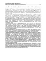
Fig. 10. Simulations and measurements of an elementary RF MEMS switch in (a) up and (b)
down positions
A good agreement between modeling and measurements is achieved for both insertion
losses (Fig. 10.a) and isolation (Fig. 10.b). These results validate the simple model used for
the RF MEMS switch. A better fit at high frequency could however be reached if additional
parasitic elements were considered, but it would highly complex the electrical model.
Depending on the technology, device architecture and targeted application, various
reliability performances under low (in the milliWatt range) and medium (in the Watt range)
power in hot or cold switching (the RF-power is on or off – respectively- during the MEMS
switching) can be found in the literature. The reliability of RF-MEMS is actually one major
concern (together with packaging issues) of the RF-MEMS researches. Considered solutions
aims to optimize as much as possible the different parameters, which limits the lifetime of
RF-MEMS devices/circuits such as:
(1) the actuation scheme of the devices. The frequency and the duty cycle of the
biasing voltage have a high impact on the MEMS reliability (Van Spengen et al.,
2002; Melle et al., 2005),
(2) the dielectric configuration, which is subject to charging. Some solutions to
decrease the charging and/or enhance the discharging have already been
proposed, such as adding holes (Goldsmith et al., 2007) or carbon-nanotubes
(Bordas et al., 2007-b) in the dielectric for examples. In any case, dielectric charging
is one major concern for high reliable RF-MEMS circuits,
(3) the thermal effects in metal lines under medium RF-power. The consequent heat
induces deformation of the mobile membrane (and even buckling), which results in
mechanical failure (Bordas et al., 2007-a),
(4) the electro-migration, as high current density, which is induced in metal line under
medium RF-power, results in alteration of metallization and then alters the
operation of the device.
As far as the elaboration of tuner is concerned, many identical MEMS structures are
required to form the complete circuit. However, some technological dispersions during the
fabrication of MEMS structures may not be totally avoided, especially the contact quality
between the metallic membrane and the MEM dielectric. Moreover as defined previously in
(Shen & Barker, 2005), capacitive ratio of 2-5:1 are required. Consequently, new MEMS
varactors, which integrate Metal-Insulator-Metal (MIM) capacitors, have been developed.
3.2 RF MEMS varactor and associated technology
Based on the previous RF-MEMS devices, MIM capacitors have been added. They are placed
between the ground planes and the membrane anchorages, as indicated in Fig. 11. They
present the high advantage of being very compact, contrary to Metal-Air-Metal (MAM)
capacitors (Vähä-Heikkilä & Rebeiz, 2004-a), but at the detriment of quality factor due to
additional dielectric losses.
Fig. 11. Cross section view and photography of a RF MEMS switch with integrated MIM
capacitors
The precedent technological process flow has consequently been modified to integrate these
MIM capacitors. Two additional steps are required. After the elaboration of the RF lines, the
MIM dielectric (Silicon Nitride) is deposited by PECVD and patterned. A top metallization
is realized by evaporation and delimited. The MEMS process restarts then with the
deposition of the MEM dielectric and continue until the final release of the structure.
Because of technological limitations, MIM capacitors have to present a value equal or higher
than 126fF.
The corresponding electrical model is slightly modified with the addition of a MIM
capacitor, as shown in
Components
Values
Line (µm) 105
LMEMS (pH) 23,5
CVAR(fF) up
down
110
500
RMEMS (Ω) up
down
2
0,15
Q@ 20GHz up
down
36
106
CMIM(fF) 450
Table 2. Electrical model of varactor with MIM capacitors
RF-MEMSbasedTunerformicrowaveandmillimeterwaveapplications 313
consequently very low losses and high isolation, with a capacitor ratio of 33. Power tests
have demonstrated that such an RF MEMS may handle up to 1W during 30 millions of
cycles in hot switching.
(a) (b)
Fig. 10. Simulations and measurements of an elementary RF MEMS switch in (a) up and (b)
down positions
A good agreement between modeling and measurements is achieved for both insertion
losses (Fig. 10.a) and isolation (Fig. 10.b). These results validate the simple model used for
the RF MEMS switch. A better fit at high frequency could however be reached if additional
parasitic elements were considered, but it would highly complex the electrical model.
Depending on the technology, device architecture and targeted application, various
reliability performances under low (in the milliWatt range) and medium (in the Watt range)
power in hot or cold switching (the RF-power is on or off – respectively- during the MEMS
switching) can be found in the literature. The reliability of RF-MEMS is actually one major
concern (together with packaging issues) of the RF-MEMS researches. Considered solutions
aims to optimize as much as possible the different parameters, which limits the lifetime of
RF-MEMS devices/circuits such as:
(1) the actuation scheme of the devices. The frequency and the duty cycle of the
biasing voltage have a high impact on the MEMS reliability (Van Spengen et al.,
2002; Melle et al., 2005),
(2) the dielectric configuration, which is subject to charging. Some solutions to
decrease the charging and/or enhance the discharging have already been
proposed, such as adding holes (Goldsmith et al., 2007) or carbon-nanotubes
(Bordas et al., 2007-b) in the dielectric for examples. In any case, dielectric charging
is one major concern for high reliable RF-MEMS circuits,
(3) the thermal effects in metal lines under medium RF-power. The consequent heat
induces deformation of the mobile membrane (and even buckling), which results in
mechanical failure (Bordas et al., 2007-a),
(4) the electro-migration, as high current density, which is induced in metal line under
medium RF-power, results in alteration of metallization and then alters the
operation of the device.
As far as the elaboration of tuner is concerned, many identical MEMS structures are
required to form the complete circuit. However, some technological dispersions during the
fabrication of MEMS structures may not be totally avoided, especially the contact quality
between the metallic membrane and the MEM dielectric. Moreover as defined previously in
(Shen & Barker, 2005), capacitive ratio of 2-5:1 are required. Consequently, new MEMS
varactors, which integrate Metal-Insulator-Metal (MIM) capacitors, have been developed.
3.2 RF MEMS varactor and associated technology
Based on the previous RF-MEMS devices, MIM capacitors have been added. They are placed
between the ground planes and the membrane anchorages, as indicated in Fig. 11. They
present the high advantage of being very compact, contrary to Metal-Air-Metal (MAM)
capacitors (Vähä-Heikkilä & Rebeiz, 2004-a), but at the detriment of quality factor due to
additional dielectric losses.
Fig. 11. Cross section view and photography of a RF MEMS switch with integrated MIM
capacitors
The precedent technological process flow has consequently been modified to integrate these
MIM capacitors. Two additional steps are required. After the elaboration of the RF lines, the
MIM dielectric (Silicon Nitride) is deposited by PECVD and patterned. A top metallization
is realized by evaporation and delimited. The MEMS process restarts then with the
deposition of the MEM dielectric and continue until the final release of the structure.
Because of technological limitations, MIM capacitors have to present a value equal or higher
than 126fF.
The corresponding electrical model is slightly modified with the addition of a MIM
capacitor, as shown in
Components
Values
Line (µm) 105
LMEMS (pH) 23,5
CVAR(fF) up
down
110
500
RMEMS (Ω) up
down
2
0,15
Q@ 20GHz up
down
36
106
CMIM(fF) 450
Table 2. Electrical model of varactor with MIM capacitors
AdvancedMicrowaveandMillimeterWave
Technologies:SemiconductorDevices,CircuitsandSystems314
The MIM capacitor's value corresponds to 450fF, which leads to varactor's values (MEM and
MIM capacitors in serial configuration) of 110 and 500fF in the up and down states
respectively. It results in a capacitive ratio of 4.5 (Bordas, 2008).
Vähä-Heikkilä et al. have proposed another solution for the reduction and control of the
capacitor ratio. They used Metal-Air-Metal (MAM) capacitors with RF-MEMS attractors (see
figure 12), which results in higher quality factor, as no dielectric losses appear in the MAM
device. This results in a 150% improvement in the off-state quality factor, a value of 154 was
indeed obtained at 20GHz (Vähä-Heikkilä & Rebeiz 2004-a) with MAM capacitors 100 times
larger than MIM ones.
Fig. 12. Metal-Air-Metal (MAM) capacitor associated with RF-MEMS varactors used for
tuning elements in tuner (Vähä-Heikkilä & Rebeiz 2004-a)
Despites these possible quality factors’ improvements, quality factors higher or around 30-
40 are sufficient to achieve low losses’ tuners, as suggested by the figure 7. RF-MEMS
devices are consequently well adapted to tuner applications (and more generally all
reconfigurable applications) as they also exhibit:
(1) Controllable and predictable capacitor ratios in the range of 2-5:1,
(2) Medium power capabilities,
(3) Compatibility with a system-on-chip approach,
(4) Low intermodulation.
The next paragraph then presents an explicit method to design an RF-MEMS-based tuner.
4. RF-MEMS Tuner Design methodology: example of the design of a building
block
4.1 Efficient Design Methodology
Thanks to the RF-MEMS-varactors and associated technology presented in the last
paragraph, we propose to detail and illustrate an explicit design methodology of TL-based
impedance tuner. The design and characterization of a basic building block of tuner: a single
stub architecture, presented in the figure 13, is detailed and discussed. The investigated
structure is composed of 3 TL sections: 2 input/output accesses and 1 stub. Each line is
loaded by 2 switchable varactors. When the loading capacitance is increased, the line
electrical length is increased and the matching is tuned. Reconfigurable varactors can be
realizable thanks to a switch, which address 2 different capacitors, or by the association of
fixed and tunable capacitors as illustrated in the figure 13.
Fig. 13. Tuner’s Topology
The parameters, which have to be optimized, are:
the MIM capacitor value : C
MIM
(we consider that the MEMS capacitor – without the
MIM- is fixed by the technological constraints),
the characteristic impedance of the unloaded line (without the varactors) : Z
0
,
the spacing s between the MEMS capacitor both for the input and the output lines
and for the stub.
It follows such targets :
an impedance coverage:
1. as uniform as possible : target 1,
2. providing high values of
: target 2,
3. providing also low values of
: target 3,
Technological feasibility (this limits some dimensions).
The target 3 is fulfilled when the characteristic impedance of the loaded line, with all
MEMS in the up position (named Z
c,up
) is close to 50 :
Z
c,up
=50
(1)
The first target is difficult to be analytically expressed. To circumvent this difficulty, we
propose to consider that this target is reached if, for each tuner’s transmission line (TL),
presented in the figure 14, the phase difference of the reflection scattering parameter (S
11
)
between the two MEMS states is 90°. Indeed, when a phase difference of 90° is reached for a
TL, an half wise rotation is observed in the Smith Chart then leading to “a best impedance
coverage”.
RF-MEMSbasedTunerformicrowaveandmillimeterwaveapplications 315
The MIM capacitor's value corresponds to 450fF, which leads to varactor's values (MEM and
MIM capacitors in serial configuration) of 110 and 500fF in the up and down states
respectively. It results in a capacitive ratio of 4.5 (Bordas, 2008).
Vähä-Heikkilä et al. have proposed another solution for the reduction and control of the
capacitor ratio. They used Metal-Air-Metal (MAM) capacitors with RF-MEMS attractors (see
figure 12), which results in higher quality factor, as no dielectric losses appear in the MAM
device. This results in a 150% improvement in the off-state quality factor, a value of 154 was
indeed obtained at 20GHz (Vähä-Heikkilä & Rebeiz 2004-a) with MAM capacitors 100 times
larger than MIM ones.
Fig. 12. Metal-Air-Metal (MAM) capacitor associated with RF-MEMS varactors used for
tuning elements in tuner (Vähä-Heikkilä & Rebeiz 2004-a)
Despites these possible quality factors’ improvements, quality factors higher or around 30-
40 are sufficient to achieve low losses’ tuners, as suggested by the figure 7. RF-MEMS
devices are consequently well adapted to tuner applications (and more generally all
reconfigurable applications) as they also exhibit:
(1) Controllable and predictable capacitor ratios in the range of 2-5:1,
(2) Medium power capabilities,
(3) Compatibility with a system-on-chip approach,
(4) Low intermodulation.
The next paragraph then presents an explicit method to design an RF-MEMS-based tuner.
4. RF-MEMS Tuner Design methodology: example of the design of a building
block
4.1 Efficient Design Methodology
Thanks to the RF-MEMS-varactors and associated technology presented in the last
paragraph, we propose to detail and illustrate an explicit design methodology of TL-based
impedance tuner. The design and characterization of a basic building block of tuner: a single
stub architecture, presented in the figure 13, is detailed and discussed. The investigated
structure is composed of 3 TL sections: 2 input/output accesses and 1 stub. Each line is
loaded by 2 switchable varactors. When the loading capacitance is increased, the line
electrical length is increased and the matching is tuned. Reconfigurable varactors can be
realizable thanks to a switch, which address 2 different capacitors, or by the association of
fixed and tunable capacitors as illustrated in the figure 13.
Fig. 13. Tuner’s Topology
The parameters, which have to be optimized, are:
the MIM capacitor value : C
MIM
(we consider that the MEMS capacitor – without the
MIM- is fixed by the technological constraints),
the characteristic impedance of the unloaded line (without the varactors) : Z
0
,
the spacing s between the MEMS capacitor both for the input and the output lines
and for the stub.
It follows such targets :
an impedance coverage:
1. as uniform as possible : target 1,
2. providing high values of
: target 2,
3. providing also low values of
: target 3,
Technological feasibility (this limits some dimensions).
The target 3 is fulfilled when the characteristic impedance of the loaded line, with all
MEMS in the up position (named Z
c,up
) is close to 50 :
Z
c,up
=50
(1)
The first target is difficult to be analytically expressed. To circumvent this difficulty, we
propose to consider that this target is reached if, for each tuner’s transmission line (TL),
presented in the figure 14, the phase difference of the reflection scattering parameter (S
11
)
between the two MEMS states is 90°. Indeed, when a phase difference of 90° is reached for a
TL, an half wise rotation is observed in the Smith Chart then leading to “a best impedance
coverage”.
AdvancedMicrowaveandMillimeterWave
Technologies:SemiconductorDevices,CircuitsandSystems316
Fig. 14. TL with tunable electrical length. This element corresponds to a generic building
block of complex tuner architectures.
To express this constraint, a parameter is introduced, which represents the two-states-
difference of the normalized length of TL, regarding the wavelength:
(2)
The impedance coverage will then be optimally uniform if:
=1/4
(3)
After some mathematical manipulations, the proposed figure of merit can be expressed as
a function of the designed parameters:
(4)
where K
up
=(Z
0
/Z
c,up
)
2
; R, s and
r0
correspond to the capacitor ratio C
down
/C
up
, the
spacing between varactors and the relative permittivity of the unloaded line respectively.
The design equation (4) then translates into an explicit expression of the capacitor ratio
(then named R
opt
), which permits to design the value of the MIM capacitors of the varactors:
(5)
(6)
The optimal value of the MIM capacitor is finally deduced from this optimal capacitor ratio
of the varactor and the up-state value of the MEMS devices (without MIM capacitor):
(7)
This last expression assumes that the MEMS capacitor ratio is large enough compared with
the one of the resulting varactor.
Finally, the target 2 is fulfilled when the down-state capacitor value of the varactor is
sufficiently large to ‘short circuit the signal’, leading to the edge of the Smith Chart. As this
value is already defined by the designed equation (4), the target 2 is optimized by tuning the
s value, which is -on the other side- constrained by the Bragg condition (Barker & Rebeiz,
1998) and the technological feasibility. The s value will then be a parameter to optimize
iteratively in order to reach the best compromise between “wide impedance coverage (i.e.
equation (1) and (4)) and “technological feasibility”.
This procedure was applied to a single-stub tuner. Considering the RF-MEMS technology
presented in the previous paragraph, the values summarized in the table 3 are reached after
some iterations and totally defines the tuner of the figure 13.
Transmission line Characteristic Impedance
63Ω
MEMS capacitor (theoretical) up
down
70 fF
4000 fF
MIM capacitor
500 fF
Total Capacitor up
down
60 fF
450 fF
Total Capacitor Ratio
7-8
Table 3. Values of the tuner’s parameters using the proposed methodology
4.2 Measured RF-Performances
The microphotography in figure 15 presents the fabricated single-stub tuner, whose
electrical parameters are given in the table 3. The integration technology used has been
developed at the LAAS-CNRS (Grenier et al. 2004; Grenier at al. 2005; Bordas, 2008) and, in
order to integrate tuners with active circuits, the RF-MEMS devices were realized on silicon
(2k.cm) with a BCB interlayer of 15 μm.
Fig. 15. Micro-photography of the fabricated RF-MEMS single stub tuner (Bordas, 2008)
The on-wafer 2-ports S parameters have been measured from 400 MHz to 30 GHz for the
2
6
=64 possible states. The DC feed lines for the varactors actuation have been regrouped and
connected to an automated DC –voltages supplier through a probe card (see figure 16).
RF-MEMSbasedTunerformicrowaveandmillimeterwaveapplications 317
Fig. 14. TL with tunable electrical length. This element corresponds to a generic building
block of complex tuner architectures.
To express this constraint, a parameter is introduced, which represents the two-states-
difference of the normalized length of TL, regarding the wavelength:
(2)
The impedance coverage will then be optimally uniform if:
=1/4
(3)
After some mathematical manipulations, the proposed figure of merit can be expressed as
a function of the designed parameters:
(4)
where K
up
=(Z
0
/Z
c,up
)
2
; R, s and
r0
correspond to the capacitor ratio C
down
/C
up
, the
spacing between varactors and the relative permittivity of the unloaded line respectively.
The design equation (4) then translates into an explicit expression of the capacitor ratio
(then named R
opt
), which permits to design the value of the MIM capacitors of the varactors:
(5)
(6)
The optimal value of the MIM capacitor is finally deduced from this optimal capacitor ratio
of the varactor and the up-state value of the MEMS devices (without MIM capacitor):
(7)
This last expression assumes that the MEMS capacitor ratio is large enough compared with
the one of the resulting varactor.
Finally, the target 2 is fulfilled when the down-state capacitor value of the varactor is
sufficiently large to ‘short circuit the signal’, leading to the edge of the Smith Chart. As this
value is already defined by the designed equation (4), the target 2 is optimized by tuning the
s value, which is -on the other side- constrained by the Bragg condition (Barker & Rebeiz,
1998) and the technological feasibility. The s value will then be a parameter to optimize
iteratively in order to reach the best compromise between “wide impedance coverage (i.e.
equation (1) and (4)) and “technological feasibility”.
This procedure was applied to a single-stub tuner. Considering the RF-MEMS technology
presented in the previous paragraph, the values summarized in the table 3 are reached after
some iterations and totally defines the tuner of the figure 13.
Transmission line Characteristic Impedance
63Ω
MEMS capacitor (theoretical) up
down
70 fF
4000 fF
MIM capacitor
500 fF
Total Capacitor up
down
60 fF
450 fF
Total Capacitor Ratio
7-8
Table 3. Values of the tuner’s parameters using the proposed methodology
4.2 Measured RF-Performances
The microphotography in figure 15 presents the fabricated single-stub tuner, whose
electrical parameters are given in the table 3. The integration technology used has been
developed at the LAAS-CNRS (Grenier et al. 2004; Grenier at al. 2005; Bordas, 2008) and, in
order to integrate tuners with active circuits, the RF-MEMS devices were realized on silicon
(2k.cm) with a BCB interlayer of 15 μm.
Fig. 15. Micro-photography of the fabricated RF-MEMS single stub tuner (Bordas, 2008)
The on-wafer 2-ports S parameters have been measured from 400 MHz to 30 GHz for the
2
6
=64 possible states. The DC feed lines for the varactors actuation have been regrouped and
connected to an automated DC –voltages supplier through a probe card (see figure 16).
AdvancedMicrowaveandMillimeterWave
Technologies:SemiconductorDevices,CircuitsandSystems318
Fig. 16. Micro-photography of the fabricated tuner under testing
The measured and simulated (with Agilent ADS) S
11
parameters vs frequency, when all the
MEMS devices are in the down position, are shown in fig. 17. This demonstrates the
accuracy of the RF-MEMS technologies’ models over a wide frequency range.
The fig. 18 presents the measured and simulated impedance coverage at 10, 12.4 and 14GHz
(64 simulated impedance values and 47 measured ones) with 50 input and output
terminations. There is a good agreement between the simulated and measured impedance
coverage with high values of
MAX
and VSWR parameters as 0.82 and 10 are respectively
obtained at 14 GHz.
Fig. 17. Measured and simulated S11 parameter, when all MEMS devices are in the down
position
measured at 10 GHz measured at 12.4 GHz measured at 14 GHz
simulated at 10 GHz simulated at 12.4 GHz simulated at 14 GHz
Fig. 18. Measured and simulated impedances coverage of the tuner at 10, 12.4 and 14 GHz
This result then validates the proposed design methodology as a wide impedance coverage
is reached after the first set of fabrication.
In term of tunable matching capability of the resulting circuit, the figure 19 presents the
input impedances of the fabricated tuner, when the output is loaded by 20 Ω. The results
demonstrate that the tuner is able to match 20 Ω on a 100 Ω input impedance (the 100 Ω
circle is drawn in the Smith Chart of the figure 19). The corresponding impedance matching
ratio of 5:1 is in the range of interest of a wide range of applications, where low noise or
power amplifiers and antennas have to be matched under different frequency ranges.
Fig. 19. Predicted input impedance coverage at 20 GHz. The output of the tuner is loaded by
20 Ω.
RF-MEMSbasedTunerformicrowaveandmillimeterwaveapplications 319
Fig. 16. Micro-photography of the fabricated tuner under testing
The measured and simulated (with Agilent ADS) S
11
parameters vs frequency, when all the
MEMS devices are in the down position, are shown in fig. 17. This demonstrates the
accuracy of the RF-MEMS technologies’ models over a wide frequency range.
The fig. 18 presents the measured and simulated impedance coverage at 10, 12.4 and 14GHz
(64 simulated impedance values and 47 measured ones) with 50 input and output
terminations. There is a good agreement between the simulated and measured impedance
coverage with high values of
MAX
and VSWR parameters as 0.82 and 10 are respectively
obtained at 14 GHz.
Fig. 17. Measured and simulated S11 parameter, when all MEMS devices are in the down
position
measured at 10 GHz measured at 12.4 GHz measured at 14 GHz
simulated at 10 GHz simulated at 12.4 GHz simulated at 14 GHz
Fig. 18. Measured and simulated impedances coverage of the tuner at 10, 12.4 and 14 GHz
This result then validates the proposed design methodology as a wide impedance coverage
is reached after the first set of fabrication.
In term of tunable matching capability of the resulting circuit, the figure 19 presents the
input impedances of the fabricated tuner, when the output is loaded by 20 Ω. The results
demonstrate that the tuner is able to match 20 Ω on a 100 Ω input impedance (the 100 Ω
circle is drawn in the Smith Chart of the figure 19). The corresponding impedance matching
ratio of 5:1 is in the range of interest of a wide range of applications, where low noise or
power amplifiers and antennas have to be matched under different frequency ranges.
Fig. 19. Predicted input impedance coverage at 20 GHz. The output of the tuner is loaded by
20 Ω.
AdvancedMicrowaveandMillimeterWave
Technologies:SemiconductorDevices,CircuitsandSystems320
5. Capabilities of RF-MEMS based tuner
The previous paragraph has presented an illustration of the design of an RF-MEMS-based
tuner in Ku and K-bands. Although the considered structure was quite simple (1-stub
topology), the measured performances in term of VSWR and impedance coverage was very
satisfactory. Of course, the presented design methodology is very generic and can also be
applied for the design of more complicated tuner architecture. The figure 20 presents a
double and triple stub tunable matching network.
Fig. 20. RF-MEMS based tuner : double and triple stub architecture
Despites the drawbacks of such structures in terms of occupied surface and insertion losses,
their impedance coverage and maximum VSWR feature improved values compare to single
stub structures. The figure 21 illustrates typical results expected from double and triple
stubs tuners and demonstrates the power of the design methodology presented in the
paragraph 4 as well as the capabilities of RF-MEMS technologies for the implementation of
integrated tuners with high performances. Excellent impedance coverage was indeed
predicted as well as high value of reflection coefficient in all the four quadrant of the Smith-
Chart.
Fig. 21. Predicted impedance coverage of a 9 bits (2 stubs) and 12 bits (3 stubs) RF-MEMS
tuner
The simulations predict for both architectures a
MAX
value of 0.95 at 20GHz, which
corresponds to a VSWR around 40. Compared with MMIC-tuner, RF-MEMS architectures
clearly exhibit improvement in term of achievable VSWR. In Ka-band, the losses of FET or
Diode limit the VSWR of tuner to 20 (McIntosh et al., 1999; Bischof, 1994), whereas as for RF-
MEMS-technology-based tuners exhibit values ranging from 32 (Kim et al., 2001) to even 199
(Vähä-Heikkilä et al., 2007). It clearly points out the breakthrough obtained by using RF-
MEMS technologies for microwave and millimeterwave tuner applications.
Moreover, the demonstration of high RF-performances of RF-MEMS-based tuner have been
successfully carried out:
1. on various architectures for
o 1-stub (Vähä-Heikkilä et al., 2004-c; Dubuc et al., 2008; Bordas, 2008; Vähä-
Heikkilä et al. 2007),
o 2-stubs (Papapolymerou et al., 2003; Kim et al., 2001; Vähä-Heikkilä et al., 2005;
Vähä-Heikkilä et al., 2007)
o 3-stubs (Vähä-Heikkilä et al., 2004-b; Vähä-Heikkilä et al., 2005; Vähä-Heikkilä
et al., 2007)
o Distributed TL (Lu et al., 2005; Qiao et al., 2005; Shen & Barker, 2005;
Lakshminarayanan & Weller, 2005; Vähä-Heikkilä & Rebeiz, 2004-a)
As anticipated (Collin, 2001), the VSWR rises when the number of stubs increases.
The table 4 presents the
MAX
and VSWR values for 1, 2 and 3-stubs RF-MEMS
tuners. Value around 40 is achieved at 16 GHz for a 3-stub structure, which
corresponds to a 100% improvement compare with a 1-stub network, but at the
expense of 70% rise of the occupied surface.
Architecture 1- stub tuner 2- stub tuner 3-stub tuner
MAX
@ 16 GHz
0,91 0,93 0,95
VSWR @ 16 GHz
21 28 39
Table 4. Γ
MAX
and VSWR vs tuner architecture (Vähä-Heikkilä et al., 2007)
2. Over a wide frequency range from 4 to 115 GHz :
o C-band (Vähä-Heikkilä & Rebeiz, 2004-a),
o X-band (Vähä-Heikkilä & Rebeiz, 2004-a; Vähä-Heikkilä et al., 2004-b; Qiao et
al., 2005),
o Ku-band(Papapolymerou et al., 2003; Vähä-Heikkilä et al., 2006),
o K-band (Dubuc et al., 2008; Bordas, 2008; Shen & Barker, 2005),
o Ka-band (Kim et al., 2001; Lu et al., 2005, Vähä-Heikkilä & Rebeiz, 2004-d),
o U and V-band (Vähä-Heikkilä et al., 2004-c)
o W-band (Vähä-Heikkilä et al., 2005)
One can notice that high values of
MAX
and VSWR are generally achieved for
high frequency operation. This is suggested by the datas reported in the table 5,
which reports a tuner with an optimized impedance coverage at 16 GHz. At this
frequency, a VSWR of 28 is measured, whereas at 30 GHz an impressive value of
199 is reported.
RF-MEMSbasedTunerformicrowaveandmillimeterwaveapplications 321
5. Capabilities of RF-MEMS based tuner
The previous paragraph has presented an illustration of the design of an RF-MEMS-based
tuner in Ku and K-bands. Although the considered structure was quite simple (1-stub
topology), the measured performances in term of VSWR and impedance coverage was very
satisfactory. Of course, the presented design methodology is very generic and can also be
applied for the design of more complicated tuner architecture. The figure 20 presents a
double and triple stub tunable matching network.
Fig. 20. RF-MEMS based tuner : double and triple stub architecture
Despites the drawbacks of such structures in terms of occupied surface and insertion losses,
their impedance coverage and maximum VSWR feature improved values compare to single
stub structures. The figure 21 illustrates typical results expected from double and triple
stubs tuners and demonstrates the power of the design methodology presented in the
paragraph 4 as well as the capabilities of RF-MEMS technologies for the implementation of
integrated tuners with high performances. Excellent impedance coverage was indeed
predicted as well as high value of reflection coefficient in all the four quadrant of the Smith-
Chart.
Fig. 21. Predicted impedance coverage of a 9 bits (2 stubs) and 12 bits (3 stubs) RF-MEMS
tuner
The simulations predict for both architectures a
MAX
value of 0.95 at 20GHz, which
corresponds to a VSWR around 40. Compared with MMIC-tuner, RF-MEMS architectures
clearly exhibit improvement in term of achievable VSWR. In Ka-band, the losses of FET or
Diode limit the VSWR of tuner to 20 (McIntosh et al., 1999; Bischof, 1994), whereas as for RF-
MEMS-technology-based tuners exhibit values ranging from 32 (Kim et al., 2001) to even 199
(Vähä-Heikkilä et al., 2007). It clearly points out the breakthrough obtained by using RF-
MEMS technologies for microwave and millimeterwave tuner applications.
Moreover, the demonstration of high RF-performances of RF-MEMS-based tuner have been
successfully carried out:
1. on various architectures for
o 1-stub (Vähä-Heikkilä et al., 2004-c; Dubuc et al., 2008; Bordas, 2008; Vähä-
Heikkilä et al. 2007),
o 2-stubs (Papapolymerou et al., 2003; Kim et al., 2001; Vähä-Heikkilä et al., 2005;
Vähä-Heikkilä et al., 2007)
o 3-stubs (Vähä-Heikkilä et al., 2004-b; Vähä-Heikkilä et al., 2005; Vähä-Heikkilä
et al., 2007)
o Distributed TL (Lu et al., 2005; Qiao et al., 2005; Shen & Barker, 2005;
Lakshminarayanan & Weller, 2005; Vähä-Heikkilä & Rebeiz, 2004-a)
As anticipated (Collin, 2001), the VSWR rises when the number of stubs increases.
The table 4 presents the
MAX
and VSWR values for 1, 2 and 3-stubs RF-MEMS
tuners. Value around 40 is achieved at 16 GHz for a 3-stub structure, which
corresponds to a 100% improvement compare with a 1-stub network, but at the
expense of 70% rise of the occupied surface.
Architecture 1- stub tuner 2- stub tuner 3-stub tuner
MAX
@ 16 GHz
0,91 0,93 0,95
VSWR @ 16 GHz
21 28 39
Table 4. Γ
MAX
and VSWR vs tuner architecture (Vähä-Heikkilä et al., 2007)
2. Over a wide frequency range from 4 to 115 GHz :
o C-band (Vähä-Heikkilä & Rebeiz, 2004-a),
o X-band (Vähä-Heikkilä & Rebeiz, 2004-a; Vähä-Heikkilä et al., 2004-b; Qiao et
al., 2005),
o Ku-band(Papapolymerou et al., 2003; Vähä-Heikkilä et al., 2006),
o K-band (Dubuc et al., 2008; Bordas, 2008; Shen & Barker, 2005),
o Ka-band (Kim et al., 2001; Lu et al., 2005, Vähä-Heikkilä & Rebeiz, 2004-d),
o U and V-band (Vähä-Heikkilä et al., 2004-c)
o W-band (Vähä-Heikkilä et al., 2005)
One can notice that high values of
MAX
and VSWR are generally achieved for
high frequency operation. This is suggested by the datas reported in the table 5,
which reports a tuner with an optimized impedance coverage at 16 GHz. At this
frequency, a VSWR of 28 is measured, whereas at 30 GHz an impressive value of
199 is reported.
AdvancedMicrowaveandMillimeterWave
Technologies:SemiconductorDevices,CircuitsandSystems322
Frequency 6 GHz 8 GHz 12 GHz 16 GHz* 20 GHz 30 GHz
MAX
0,95 0,94 0,91 0,93 0,96 0,99
VSWR
39 32 21 28 49 199
* Optimal impedance coverage of the Smith-Chart
Table 5.
MAX
and VSWR vs frequency for a 2-stubs tuner (Vähä-Heikkilä et al., 2007)
A tradeoff between impedance coverage and high value of
MAX
and VSWR then
exists and both features need to be considered for fair comparison.
6. Conclusions
This chapter has presented the design, technology and performances of RF-MEMS-based
tuners. Various architectures have been presented in order to give a large overview of tuner-
topologies. An efficient and explicit design methodology has been explained and illustrated
through a practical example. The authors have moreover outlined the potential of RF-MEMS
technologies for different applications (tunable impedance matching between integrated
functions within smart microsystems, wide impedance values generations for devices
characterization) because of their ability for IC-co-integration, low losses performances and
low distortion characteristics.
7. Acknowledgements
The authors would like to specifically acknowledge Chloe Bordas, who was Ph.D student
under the supervision of Katia Grenier and David Dubuc from 2005 to 2008 and worked on
RF-MEMS based tuner. She was an essential backbone of the work presented in this
Chapter.
We also would like to thanks Samuel Melle, Benoît Ducarouge and Jean-Pierre Busquere,
Ph. D students under the supervision of David Dubuc and Katia Grenier from 2002 to 2005.
Their work on RF-MEMS design, fabrication and reliability contributed to rise the
knowledge of the team, and permit to envision circuits based on RF-MEMS varactors.
Katia Grenier and David Dubuc also acknowledge the support of Thales Alenia Space, the
French Defense Agency (DGA) and ST-Microelectronics.
8. References
Barker, S. Rebeiz, G.M. (1998). Distributed MEMS true-time delay phase shifters and wide-band
switches. IEEE Transactions on Microwave Theory and Techniques, Vol. 46, Issue 11, Part 2,
Nov. 1998 pp:1881 – 1890
Bischof, W. (1994). Variable impedance tuner for MMIC's. Microwave and Guided Wave Letters,
Volume 4, Issue 6, June 1994 Page(s):172 – 174
Bordas, C.; Grenier, K.; Dubuc, D.; Paillard, M.; Cazaux, J L.; et al. (2007-a). Temperature stress
impact on power RF MEMS switches, Microtechnologies for the new millennium 2007,
Smart sensors, actuators and MEMS, Maspalomas, Espagne. Mai 2007.
Bordas, C.; Grenier, K.; Dubuc, D.; Flahaut, E.; Pacchini, S. Paillard, M.; Cazaux, J-L. (2007-b).
Carbon nanotube based dielectric for enhanced RF MEMS reliability. IEEE/MTT-S
International Microwave Symposium, June 2007.
Bordas, C. (2008). Technological optimization of RF MEMS switches with enhanced power
handling – Elaboration of a MEMS-based impedance tuner in K-band. Ph.D. dissertation
(in French), April 2008.
Busquere, J P.; Grenier, K.; Dubuc, D.; Fourn, E.; Ancey, P.; et al. (2006). MEMS IC concept for
Reconfigurable Low Noise Amplifier. 36th European,Microwave Conference, 2006. 10-15
Sept. 2006 Page(s):1358 - 1361
Collin, R. E. (2001). Field Theory of Guided Waves, 2nd ed., IEEE Press.
Dubuc, D.; Saddaoui, M; Melle, S.; Flourens, F.; Rabbia, L.; Ducarouge, B.; Grenier, K.; et al.
(2004). Smart MEMS concept for high secure RF and millimeterwave communications.
Microelectronics Reliability, Volume 44, Issue 6, June 2004, Pages 899-907
Dubuc, D.; Bordas , C.; Grenier, K. (2008). Efficient design methodology of RF-MEMS based
tuner. European Microwave Week 2008 (EuMW 2008), Amsterdam (Pays Bas), 27-31
Octobre 2008, pp.398-401
Ducarouge, B.; Dubuc, D.; Melle, S.; Bary, L.; Pons, P.; et al. (2004). Efficient design methodology
of polymer based RF MEMS switches. 2004 Topical Meeting on Silicon Monolithic
Integrated Circuits in RF Systems, 2004. 8-10 Sept. 2004 Page(s):298 – 301
Goldsmith, C.L.; Forehand, D.I.; Peng, Z.; Hwang, J.C.M.; Ebel, I.L. (2007). High-Cycle Life
Testing of RF MEMS Switches. IEEE/MTT-S International Microwave Symposium, 2007. 3-
8 June 2007 Page(s):1805 – 1808.
Grenier, K.; Dubuc, D.; Mazenq, L.; Busquère, J-P.; Ducarouge, B.; Bouchriha, F.; Rennane, M.;
Lubecke, V.; et al. (2004). Polymer based technologies for microwave and
millimeterwave applications. 50
th
IEEE International Electron Devices Meeting, 2004, San
Francisco, USA, Dec. 2004.
Grenier, K.; Dubuc, D.; Ducarouge, B.; Conedera, V.; Bourrier, D.; Ongareau, E.; Derderian, P.; et
al. (2005). High power handling RF MEMS design and technology. 18th IEEE
International Conference on Micro Electro Mechanical Systems, 2005. 30 Jan 3 Feb. 2005
Page(s):155 – 158
Grenier, K.; Bordas, C. Pinaud, S.; Salvagnac, L.; Dubuc, D. (2007). Germanium resistors for RF
MEMS based Microsystems. Microsystems Technologies, DOI 10.1007/s00542-007-0448-4.
Kim, H T.; Jung, S.; Kang, K.; Park, J H.; Kim, Y K.; Kwon Y. (2001). Low-loss analog and digital
micromachined impedance tuners at the Ka-band. IEEE Transactions on Microwave
Theory and Techniques, December 2001, Vol. 49, No. 12, pp. 2394-2400.
Lakshminarayanan, B.; Weller, T. (2005). Reconfigurable MEMS transmission lines with
independent Z0- and β- tuning. IEEE/MTT-S International Microwave Symposium, 2005.
Lu, Y.; Katehi, L. P. B.; Peroulis D. (2005). High-power MEMS varactors and impedance tuners
for millimeter-wave applications. IEEE Transactions on Microwave Theory and Techniques,
November 2005, Vol. 53, No. 11, pp. 3672-3678.
McIntosh, C.E.; Pollard, R.D.; Miles, R.E. (1999). Novel MMIC source-impedance tuners for on-
wafer microwave noise-parameter measurements. IEEE Transactions on Microwave
Theory and Techniques, Volume 47, Issue 2, Feb. 1999 Page(s):125 – 131
Melle, S.; De Conto, D.; Dubuc, D.; Grenier, K.; Vendier, O.; Muraro, J L.; Cazaux, J L.; et al.
(2005). Reliability modeling of capacitive RF MEMS. IEEE Transactions on Microwave
Theory and Techniques, Volume 53, Issue 11, Nov. 2005 Page(s):3482 - 3488
RF-MEMSbasedTunerformicrowaveandmillimeterwaveapplications 323
Frequency 6 GHz 8 GHz 12 GHz 16 GHz* 20 GHz 30 GHz
MAX
0,95 0,94 0,91 0,93 0,96 0,99
VSWR
39 32 21 28 49 199
* Optimal impedance coverage of the Smith-Chart
Table 5.
MAX
and VSWR vs frequency for a 2-stubs tuner (Vähä-Heikkilä et al., 2007)
A tradeoff between impedance coverage and high value of
MAX
and VSWR then
exists and both features need to be considered for fair comparison.
6. Conclusions
This chapter has presented the design, technology and performances of RF-MEMS-based
tuners. Various architectures have been presented in order to give a large overview of tuner-
topologies. An efficient and explicit design methodology has been explained and illustrated
through a practical example. The authors have moreover outlined the potential of RF-MEMS
technologies for different applications (tunable impedance matching between integrated
functions within smart microsystems, wide impedance values generations for devices
characterization) because of their ability for IC-co-integration, low losses performances and
low distortion characteristics.
7. Acknowledgements
The authors would like to specifically acknowledge Chloe Bordas, who was Ph.D student
under the supervision of Katia Grenier and David Dubuc from 2005 to 2008 and worked on
RF-MEMS based tuner. She was an essential backbone of the work presented in this
Chapter.
We also would like to thanks Samuel Melle, Benoît Ducarouge and Jean-Pierre Busquere,
Ph. D students under the supervision of David Dubuc and Katia Grenier from 2002 to 2005.
Their work on RF-MEMS design, fabrication and reliability contributed to rise the
knowledge of the team, and permit to envision circuits based on RF-MEMS varactors.
Katia Grenier and David Dubuc also acknowledge the support of Thales Alenia Space, the
French Defense Agency (DGA) and ST-Microelectronics.
8. References
Barker, S. Rebeiz, G.M. (1998). Distributed MEMS true-time delay phase shifters and wide-band
switches. IEEE Transactions on Microwave Theory and Techniques, Vol. 46, Issue 11, Part 2,
Nov. 1998 pp:1881 – 1890
Bischof, W. (1994). Variable impedance tuner for MMIC's. Microwave and Guided Wave Letters,
Volume 4, Issue 6, June 1994 Page(s):172 – 174
Bordas, C.; Grenier, K.; Dubuc, D.; Paillard, M.; Cazaux, J L.; et al. (2007-a). Temperature stress
impact on power RF MEMS switches, Microtechnologies for the new millennium 2007,
Smart sensors, actuators and MEMS, Maspalomas, Espagne. Mai 2007.
Bordas, C.; Grenier, K.; Dubuc, D.; Flahaut, E.; Pacchini, S. Paillard, M.; Cazaux, J-L. (2007-b).
Carbon nanotube based dielectric for enhanced RF MEMS reliability. IEEE/MTT-S
International Microwave Symposium, June 2007.
Bordas, C. (2008). Technological optimization of RF MEMS switches with enhanced power
handling – Elaboration of a MEMS-based impedance tuner in K-band. Ph.D. dissertation
(in French), April 2008.
Busquere, J P.; Grenier, K.; Dubuc, D.; Fourn, E.; Ancey, P.; et al. (2006). MEMS IC concept for
Reconfigurable Low Noise Amplifier. 36th European,Microwave Conference, 2006. 10-15
Sept. 2006 Page(s):1358 - 1361
Collin, R. E. (2001). Field Theory of Guided Waves, 2nd ed., IEEE Press.
Dubuc, D.; Saddaoui, M; Melle, S.; Flourens, F.; Rabbia, L.; Ducarouge, B.; Grenier, K.; et al.
(2004). Smart MEMS concept for high secure RF and millimeterwave communications.
Microelectronics Reliability, Volume 44, Issue 6, June 2004, Pages 899-907
Dubuc, D.; Bordas , C.; Grenier, K. (2008). Efficient design methodology of RF-MEMS based
tuner. European Microwave Week 2008 (EuMW 2008), Amsterdam (Pays Bas), 27-31
Octobre 2008, pp.398-401
Ducarouge, B.; Dubuc, D.; Melle, S.; Bary, L.; Pons, P.; et al. (2004). Efficient design methodology
of polymer based RF MEMS switches. 2004 Topical Meeting on Silicon Monolithic
Integrated Circuits in RF Systems, 2004. 8-10 Sept. 2004 Page(s):298 – 301
Goldsmith, C.L.; Forehand, D.I.; Peng, Z.; Hwang, J.C.M.; Ebel, I.L. (2007). High-Cycle Life
Testing of RF MEMS Switches. IEEE/MTT-S International Microwave Symposium, 2007. 3-
8 June 2007 Page(s):1805 – 1808.
Grenier, K.; Dubuc, D.; Mazenq, L.; Busquère, J-P.; Ducarouge, B.; Bouchriha, F.; Rennane, M.;
Lubecke, V.; et al. (2004). Polymer based technologies for microwave and
millimeterwave applications. 50
th
IEEE International Electron Devices Meeting, 2004, San
Francisco, USA, Dec. 2004.
Grenier, K.; Dubuc, D.; Ducarouge, B.; Conedera, V.; Bourrier, D.; Ongareau, E.; Derderian, P.; et
al. (2005). High power handling RF MEMS design and technology. 18th IEEE
International Conference on Micro Electro Mechanical Systems, 2005. 30 Jan 3 Feb. 2005
Page(s):155 – 158
Grenier, K.; Bordas, C. Pinaud, S.; Salvagnac, L.; Dubuc, D. (2007). Germanium resistors for RF
MEMS based Microsystems. Microsystems Technologies, DOI 10.1007/s00542-007-0448-4.
Kim, H T.; Jung, S.; Kang, K.; Park, J H.; Kim, Y K.; Kwon Y. (2001). Low-loss analog and digital
micromachined impedance tuners at the Ka-band. IEEE Transactions on Microwave
Theory and Techniques, December 2001, Vol. 49, No. 12, pp. 2394-2400.
Lakshminarayanan, B.; Weller, T. (2005). Reconfigurable MEMS transmission lines with
independent Z0- and β- tuning. IEEE/MTT-S International Microwave Symposium, 2005.
Lu, Y.; Katehi, L. P. B.; Peroulis D. (2005). High-power MEMS varactors and impedance tuners
for millimeter-wave applications. IEEE Transactions on Microwave Theory and Techniques,
November 2005, Vol. 53, No. 11, pp. 3672-3678.
McIntosh, C.E.; Pollard, R.D.; Miles, R.E. (1999). Novel MMIC source-impedance tuners for on-
wafer microwave noise-parameter measurements. IEEE Transactions on Microwave
Theory and Techniques, Volume 47, Issue 2, Feb. 1999 Page(s):125 – 131
Melle, S.; De Conto, D.; Dubuc, D.; Grenier, K.; Vendier, O.; Muraro, J L.; Cazaux, J L.; et al.
(2005). Reliability modeling of capacitive RF MEMS. IEEE Transactions on Microwave
Theory and Techniques, Volume 53, Issue 11, Nov. 2005 Page(s):3482 - 3488
AdvancedMicrowaveandMillimeterWave
Technologies:SemiconductorDevices,CircuitsandSystems324
Papapolymerou, J.; Lange, K.L.; Goldsmith, C.L.; Malczewski, A.; Kleber, J. (2003).
Reconfigurable double-stub tuners using MEMS switches for intelligent RF front-end.
IEEE Transactions on Microwave Theory and Techniques, Volume 51, Issue 1, Part 2, Jan.
2003 Page(s):271 - 278
Pozar, D.M. (2005). Microwave Engineering. 3rd ed., Wiley 2005.
Qiao, D.; Molfino, R.; Lardizabal, S.M.; Pillans, B.; Asbeck, P.M.; Jerinic, G. (2005). An intelligently
controlled RF power amplifier with a reconfigurable MEMS-varactor tuner. IEEE
Transactions on Microwave Theory and Techniques, Volume 53, Issue 3, Part 2, March
2005 Page(s):1089 - 1095
Rebeiz, G. M. (2003). RF MEMS: Theory, Design, and Technology. New York: Wiley, 2003.
Shen, Q; Baker, N.S. (2005). A reconfigurable RF MEMS based double slug impedance tuner.
European Microwave Conference 2005, Paris, pp. 537-540.
Tagro, Y.; Gloria, D.; Boret, S.; Morandini, Y.; Dambrine, G. (2008). In-situ silicon integrated tuner
for automated on-wafer MMW noise parameters extraction of Si HBT and MOSFET in
the range 60–110GHz. 72
nd
ARFTG Microwave Measurement Symposium, 2008. 9-12 Dec.
2008 Page(s):119 – 122
Van Spengen, W.M.; Puers, R.; Mertens, R.; De Wolf, I. (2002). Experimental characterization of
stiction due to charging in RF MEMS. International Electron Devices Meeting, 2002. IEDM
'02. Digest. 8-11 Dec. 2002 Page(s):901 – 904
Vähä-Heikkilä, T.; Rebeiz, G.M. (2004-a). A 4-18-GHz reconfigurable RF MEMS matching
network for power amplifier applications. International Journal of RF and Microwave
Computer-Aided Engineering. Volume 14 Issue 4, Pages 356 – 372. 9 Jun 2004
Vähä-Heikkilä, T.; Varis, J.; Tuovinen, J.; Rebeiz, G. M. (2004-b). A reconfigurable 6-20 GHz RF
MEMS impedance tuner”. IEEE/MTT-S International Microwave Symposium, 2004, pp.
729-732.
Vähä-Heikkilä, T.; Varis, J.; Tuovinen, J.; Rebeiz, G.M. (2004-c). A V-band single-stub RF MEMS
impedance tuner. 34th European Microwave Conference, 2004, Volume 3, 11-15 Oct. 2004
Page(s):1301 – 1304
Vähä-Heikkilä, T.; Rebeiz, G. M. (2004-d). A 20-50 GHz reconfigurable matching network for
power amplifier applications. IEEE/MTT-S International Microwave Symposium, 2004, pp.
717-720.
Vähä-Heikkilä, T.; Varis, J.; Tuovinen, J.; Rebeiz, G.M. (2005).W-band RF MEMS double and
triple-stub impedance tuners. IEEE/MTT-S International Microwave Symposium, 12-17
June 2005
Vähä-Heikkilä, T.; Caekenberghe, K.V.; Varis,J.; Tuovinen, J.; Rebeiz, G.M. (2007). RF MEMS
Impedance Tuners for 6-24 GHz Applications. International Journal of RF and Microwave
Computer-Aided Engineering, 26 Mar 2007, Volume 17 Issue 3, Pages 265 – 278.
BroadbandGaNMMICPowerAmpliersdesign 325
BroadbandGaNMMICPowerAmpliersdesign
María-ÁngelesGonzález-GarridoandJesúsGrajal
x
Broadband GaN MMIC Power
Amplifiers design
María-Ángeles González-Garrido and Jesús Grajal
Departamento de Señales, Sistemas y Radiocomunicaciones, ETSIT, Universidad
Politécnica de Madrid, Ciudad Universitaria s/n, 28040, Madrid, Spain
1. Introduction
Monolithic microwave integrated circuits (MMIC) based on gallium nitride (GaN) high
electron mobility transistors (HEMT) have the advantage of providing broadband power
performance (Milligan et al., 2007). The high breakdown voltage and high current density of
GaN devices provide higher power density than the traditional technology based on GaAs.
This allows the use of smaller devices for the same output power, and since impedance is
higher for smaller devices, broadband matching becomes easier.
In this chapter, we summarise the design procedure of broadband MMIC high power
amplifiers (HPA). Although the strategy is quite similar for most semiconductors used in
HPAs, some special considerations, as well as, experimental results will be focused on GaN
technology.
Apart from design considerations to achieve the desired RF response, it is essential to
analyse the stability of the designed HPA to guarantee that no oscillation phenomena arises.
In first place, the transistors are analysed using Rollet's linear K factor. Next, it is also critical
to perform nonlinear parametric and odd stability studies under high power excitation. The
strategy adopted for this analysis is based on pole-zero identification of the frequency
response obtained at critical nodes of the final circuit (Barquinero et al., 2007).
Finally, to avoid irreversible device degradation, thermal simulations are required to
accurately predict the highest channel temperature and thermal coupling between
transistors.
2. AlGaN/GaN HEMT Technology
First of all, MMIC GaN technology has to be evaluated. High power GaN devices operate at
high temperature and high-dissipated power due to the high power density of performance.
Therefore, the use of substrates with high thermal conductivity like the silicon carbide (SiC)
is preferred.
GaN technological process is still immature and complex. However, gate lithography
resolution lower than 0.2 μm and AlGaN/GaN epi-structures on 100-mm SiC substrates are
already available (Milligan et al., 2007).
16
AdvancedMicrowaveandMillimeterWave
Technologies:SemiconductorDevices,CircuitsandSystems326
W
i
m
i
se
m
ve
l
tr
a
de
co
m
Fi
g
T
h
di
m
Fi
g
In
di
f
th
e
hi
g
T
h
di
s
Fi
g
i
de band gap se
m
i
crowave hi
g
h
p
m
iconductors, G
a
l
ocit
y
(v
sat
), an
a
nsistors (HEMT
s
nsit
y
and the hi
g
m
pared to SiC
m
g
. 1 summarizes
G
h
is technolo
gy
h
m
ensions of 0.55
x
g
. 1. GaN HEMT
a HEMT the co
n
f
ferent band gap
.
e
electrons, resul
t
g
h sheet carrier
d
h
e spontaneous
a
s
tribution in the
A
g
. 2. AlGaN/Ga
N
m
iconductors su
c
p
ower devices.
T
a
As and Si, incl
u
d hi
g
h therma
l
s
) offer even hi
g
g
her saturation v
e
m
etal semicondu
c
G
aN-HEMT pro
p
h
as demonstrate
d
x
246 μm
2
at 4 G
H
properties and b
e
n
duction channel
.
This re
g
io
n
kn
o
t
in
g
in a ver
y
hi
g
d
ensit
y
in the 2D
E
a
nd piezoelectric
A
lGaN/GaN HE
M
N
HEMT model.
c
h as GaN and
S
T
he advanta
g
es
u
de hi
g
h breakd
o
l
conductivit
y
.
g
her power perf
o
e
locit
y
of the bid
i
c
tor field effect
t
p
erties and its be
n
d
a power den
s
H
z when biased a
t
e
nefits.
is confined to t
h
o
wn as 2DEG ha
s
g
h mobilit
y
devi
c
E
G interface wit
h
polarization eff
M
T (Ambacher e
S
iC are ver
y
pro
m
of these mater
i
o
wn field (E
g
),
h
GaN/AlGaN
h
o
rmance due to t
i
mensional elect
r
t
ransistors (MES
n
efits.
s
it
y
of 30 W/m
m
t
120 V (Wu et al.
,
h
e interface betw
e
s
ver
y
few ioniz
e
c
e. AlGaN/GaN
h
h
out intentional
d
e
cts are the ke
y
t al., 2000).
m
isin
g
technolo
g
i
als over conve
n
h
i
g
h saturation e
l
h
i
g
h electron
m
he hi
g
her carrie
r
r
on
g
as channel (
2
FETs). The dia
gr
m
usin
g
device
s
,
2004).
e
en two materia
l
e
d impurities to
h
eterostructures
d
opin
g
of the str
u
factors for the
c
g
ies for
n
tional
l
ectron
m
obilit
y
r
sheet
2
DEG)
r
am in
s
with
l
s with
scatter
have a
u
cture.
c
har
g
e
The model of a HEMT that shows the small-signal parameters and the 2DEG channel is
depicted in Fig. 2. Source and drain ohmic contact, as well as Schottky gate can be observed.
The gate voltage (V
gs
) controls the current (I
ds
) that flows between the source and the drain.
When V
gs
reaches pinch-off voltage the electrons below the gate are depleted and no current
can flow from drain to source.
Since AlGaN/GaN HEMTs for HPA applications work under high power conditions, non-
linear models have to be used to simulate the transistor performance. The success of the
design depends on the precision of the model fitting. A widely used approach is based on
Angelov analytical expressions (Angelov et al., 1992). The model parameters are extracted
from load pull, S-parameters, and pulse IV measurements. For instance, the nonlinear
current source is characterized fitting DC and pulsed IV-measurements. The voltage
controlled gate-source and gate-drain capacitance functions (C
gs
and C
gd
) are determined
from bias dependent hot-FET S-parameter measurements. Finally, the parasitic elements of
the HEMT model are extracted with cold-FET S-parameters measured from pinch-off to
open channel bias conditions. The high temperature performance of GaN-HPAs demands
the use of electro-thermal models (
Nuttinck et al., 2003). Otherwise, power estimation will
be too optimistic in CW operation.
The design methodology evaluated in this chapter is based on the experience reported by
the design of several 2-6 GHz HPAs. The active devices used are 1-mm gate-periphery
HEMTs fabricated using AlGaN/GaN heterostructures and gate length (L
g
) technology of
0.5 μm from Selex Sistemi Integrati S.p.A foundry (Costrini et al., 2008) within Korrigan
project (Gauthier et al., 2005). The HEMT cells consist of 10 fingers, each with a unit gate
width (Wg) of 100 μm. The maximum measured oscillation frequency (f
max
) of these
transistors is about 39 GHz.
A considerable dispersion between wafers is still observed because of GaN technology
immaturity. Table 1 shows the main characteristics (device maximum current I
dss
, pinch-off
voltage V
p
, breakdown voltage V
bgd
, C
gs
, sheet resistance R
s
and contact resistance R
c
) of two
wafers fabricated for the 2-6 GHz HPAs (wafer 1 and 2) and the wafer used for extracting
the nonlinear electrical models (wafer 0) for the 1
st
-run designs. From the results in Table 1,
an important deviation between the model and the measurements is expected. For instance,
Cgs mismatch will produce a poor S11 fitting.
Wafer
I
dss
mA/mm
V
p
(V)
V
bgd
(V)
C
gs
(pF/mm)
R
s
(Ω/sq)
R
c
(Ωmm)
Wafer 0 972 -6.4 >70 3.2 355 0.44
Wafer 1 794 -4.7 50 2.24 456 0.47
Wafer 2 567 -2.7 71 2.88 440 0.36
Table 1. GaN wafers comparison.
Regarding passive technology, the foundries provide microstrip and coplanar models for
typical MMIC components such as transmission lines, junctions, inductors, MIM capacitors
and both NiCr and GaN resistors.
3. Design
The design process of a broadband HPA is described in this section. Special attention should
be paid on broadband matching network synthesis and device stability.
BroadbandGaNMMICPowerAmpliersdesign 327
W
i
m
i
se
m
ve
l
tr
a
de
co
m
Fi
g
T
h
di
m
Fi
g
In
di
f
th
e
hi
g
T
h
di
s
Fi
g
i
de band gap se
m
i
crowave hi
g
h
p
m
iconductors, G
a
l
ocit
y
(v
sat
), an
a
nsistors (HEMT
s
nsit
y
and the hi
g
m
pared to SiC
m
g
. 1 summarizes
G
h
is technolo
gy
h
m
ensions of 0.55
x
g
. 1. GaN HEMT
a HEMT the co
n
f
ferent band gap
.
e
electrons, resul
t
g
h sheet carrier
d
h
e spontaneous
a
s
tribution in the
A
g
. 2. AlGaN/Ga
N
m
iconductors su
c
p
ower devices.
T
a
As and Si, incl
u
d hi
g
h therma
l
s
) offer even hi
g
g
her saturation v
e
m
etal semicondu
c
G
aN-HEMT pro
p
h
as demonstrate
d
x
246 μm
2
at 4 G
H
properties and b
e
n
duction channel
.
This re
g
io
n
kn
o
t
in
g
in a ver
y
hi
g
d
ensit
y
in the 2D
E
a
nd piezoelectric
A
lGaN/GaN HE
M
N
HEMT model.
c
h as GaN and
S
T
he advanta
g
es
u
de hi
g
h breakd
o
l
conductivit
y
.
g
her power perf
o
e
locit
y
of the bid
i
c
tor field effect
t
p
erties and its be
n
d
a power den
s
H
z when biased a
t
e
nefits.
is confined to t
h
o
wn as 2DEG ha
s
g
h mobilit
y
devi
c
E
G interface wit
h
polarization eff
M
T (Ambacher e
S
iC are ver
y
pro
m
of these mater
i
o
wn field (E
g
),
h
GaN/AlGaN
h
o
rmance due to t
i
mensional elect
r
t
ransistors (MES
n
efits.
s
it
y
of 30 W/m
m
t
120 V (Wu et al.
,
h
e interface betw
e
s
ver
y
few ioniz
e
c
e. AlGaN/GaN
h
h
out intentional
d
e
cts are the ke
y
t al., 2000).
m
isin
g
technolo
g
i
als over conve
n
h
i
g
h saturation e
l
h
i
g
h electron
m
he hi
g
her carrie
r
r
on
g
as channel (
2
FETs). The dia
gr
m
usin
g
device
s
,
2004).
e
en two materia
l
e
d impurities to
h
eterostructures
d
opin
g
of the str
u
factors for the
c
g
ies for
n
tional
l
ectron
m
obilit
y
r
sheet
2
DEG)
r
am in
s
with
l
s with
scatter
have a
u
cture.
c
har
g
e
The model of a HEMT that shows the small-signal parameters and the 2DEG channel is
depicted in Fig. 2. Source and drain ohmic contact, as well as Schottky gate can be observed.
The gate voltage (V
gs
) controls the current (I
ds
) that flows between the source and the drain.
When V
gs
reaches pinch-off voltage the electrons below the gate are depleted and no current
can flow from drain to source.
Since AlGaN/GaN HEMTs for HPA applications work under high power conditions, non-
linear models have to be used to simulate the transistor performance. The success of the
design depends on the precision of the model fitting. A widely used approach is based on
Angelov analytical expressions (Angelov et al., 1992). The model parameters are extracted
from load pull, S-parameters, and pulse IV measurements. For instance, the nonlinear
current source is characterized fitting DC and pulsed IV-measurements. The voltage
controlled gate-source and gate-drain capacitance functions (C
gs
and C
gd
) are determined
from bias dependent hot-FET S-parameter measurements. Finally, the parasitic elements of
the HEMT model are extracted with cold-FET S-parameters measured from pinch-off to
open channel bias conditions. The high temperature performance of GaN-HPAs demands
the use of electro-thermal models (
Nuttinck et al., 2003). Otherwise, power estimation will
be too optimistic in CW operation.
The design methodology evaluated in this chapter is based on the experience reported by
the design of several 2-6 GHz HPAs. The active devices used are 1-mm gate-periphery
HEMTs fabricated using AlGaN/GaN heterostructures and gate length (L
g
) technology of
0.5 μm from Selex Sistemi Integrati S.p.A foundry (Costrini et al., 2008) within Korrigan
project (Gauthier et al., 2005). The HEMT cells consist of 10 fingers, each with a unit gate
width (Wg) of 100 μm. The maximum measured oscillation frequency (f
max
) of these
transistors is about 39 GHz.
A considerable dispersion between wafers is still observed because of GaN technology
immaturity. Table 1 shows the main characteristics (device maximum current I
dss
, pinch-off
voltage V
p
, breakdown voltage V
bgd
, C
gs
, sheet resistance R
s
and contact resistance R
c
) of two
wafers fabricated for the 2-6 GHz HPAs (wafer 1 and 2) and the wafer used for extracting
the nonlinear electrical models (wafer 0) for the 1
st
-run designs. From the results in Table 1,
an important deviation between the model and the measurements is expected. For instance,
Cgs mismatch will produce a poor S11 fitting.
Wafer
I
dss
mA/mm
V
p
(V)
V
bgd
(V)
C
gs
(pF/mm)
R
s
(Ω/sq)
R
c
(Ωmm)
Wafer 0 972 -6.4 >70 3.2 355 0.44
Wafer 1 794 -4.7 50 2.24 456 0.47
Wafer 2 567 -2.7 71 2.88 440 0.36
Table 1. GaN wafers comparison.
Regarding passive technology, the foundries provide microstrip and coplanar models for
typical MMIC components such as transmission lines, junctions, inductors, MIM capacitors
and both NiCr and GaN resistors.
3. Design
The design process of a broadband HPA is described in this section. Special attention should
be paid on broadband matching network synthesis and device stability.
AdvancedMicrowaveandMillimeterWave
Technologies:SemiconductorDevices,CircuitsandSystems328
3.1 Amplifiers Topology
The first step in an HPA design is to choose the most appropriated topology to fulfil design
specifications. Single or multi-stage topology will be used depending on the gain target. In
order to achieve high output power, several devices must be combined in parallel.
The classical combination topologies are the balanced and the corporative HPA. Balanced
structures are made with λ/4-lines, which become quite large in designs below X-band.
Furthermore, multi-stage approach for broadband design will enlarge the circuit even more.
On the other hand, the corporate topology based on two-way splitters seems to be a more
versatile solution for broadband designs. It can be designed with compact lumped
broadband filters in frequencies below X-band while transmission lines can be used at
higher frequencies.
Fig. 3. Two-stage corporative topology amplifier.
The two-stage corporative topology, such as the one in Fig. 3, is widely used to design
HPAs, because it offers a good compromise between gain and power. Note that the first
stage consists of two unit cells which drive the output stage, composed of four equal cells.
This power amplifier has three matching networks: input-, inter-, and output-stage. The
labels displayed in Fig. 3 represent the loss of each matching network (L
i
), the number of
combined cells (N
i
), the power added efficiency (PAE
i
), the gain (G
i
), and the output power
(P
i
) at the i
th
-stage.
Output stage loss, L
3
, is critical to the HPA output power (P
out
=N· P
HEMT
· L
3
). Besides,
network loss has to be minimised mainly in the output network, because it is essential to
maximise power added efficiency (PAE
total
). Equation (1) is used to calculate PAE
total
of a
corporative topology with 2
n
transistors at the output stage. The representation of equation
(1) in Fig. 4 confirms the higher influence of L
3
in PAE
total
.
ܲܣܧ
௧௧
ൌ
ா
భ
ா
మ
ሺ
భ
మ
య
ீ
భ
ீ
మ
ିଵሻ
ா
భ
భ
మ
ீ
భ
ሺீ
మ
ିଵሻାா
మ
భ
ሺீ
భ
ିଵሻ
(1)
Fig. 4. PAE
total
versus input-, inter-, and output-stage network loss. To analyse the influence
of each network the loss of the other networks are set to 0 dB.
High efficiency operation is especially important for power devices, because thermal issues
can degrade the amplifier performance. Dissipated power (P
dis
) is inversely proportional to
the HPA efficiency, see equation (2).
P
dis
≈ P
out
· ((PAE
total
)
-1
- 1)
(2)
P
dis
and temperature increase (∆T) are related in equation (3) through the thermal resistance
(R
th
). This parameter gives an idea of the thermal flow through a material or a stack of
materials from a hot spot to another observation point. Therefore, R
th
depends on the
thermal conductivity of the materials and the final HPA set-up.
(3)
3.2 Unit transistor cell
The unit transistor cell size selection is based on a compromise between gain and power,
because large devices have higher power, but lower gain (Walker, 1993). Moreover, input
and output impedances decrease for larger devices, making the design of broadband
matching networks difficult. The lack of power of small devices can be solved by combining
several devices in parallel. It is worth noting that the complexity of the design increases with
the number of cells to be combined.
Once the transistor size is selected, the available unit cells have to be evaluated at different
bias operating conditions (Snider, 1967). The optimum operation class of a power amplifier
depends on the linearity, efficiency or complexity of the design specifications. In the
conventional operation classes, A, B, AB and C, the transistor works like a voltage controlled
current source. On the contrary, there are some other classes, such as D, E and F, where
amplifier efficiency improves by working like a switch. In the diagram of Fig. 5, different
operation classes have been represented, indicating the IV-curves, the load-lines and the
BroadbandGaNMMICPowerAmpliersdesign 329
3.1 Amplifiers Topology
The first step in an HPA design is to choose the most appropriated topology to fulfil design
specifications. Single or multi-stage topology will be used depending on the gain target. In
order to achieve high output power, several devices must be combined in parallel.
The classical combination topologies are the balanced and the corporative HPA. Balanced
structures are made with λ/4-lines, which become quite large in designs below X-band.
Furthermore, multi-stage approach for broadband design will enlarge the circuit even more.
On the other hand, the corporate topology based on two-way splitters seems to be a more
versatile solution for broadband designs. It can be designed with compact lumped
broadband filters in frequencies below X-band while transmission lines can be used at
higher frequencies.
Fig. 3. Two-stage corporative topology amplifier.
The two-stage corporative topology, such as the one in Fig. 3, is widely used to design
HPAs, because it offers a good compromise between gain and power. Note that the first
stage consists of two unit cells which drive the output stage, composed of four equal cells.
This power amplifier has three matching networks: input-, inter-, and output-stage. The
labels displayed in Fig. 3 represent the loss of each matching network (L
i
), the number of
combined cells (N
i
), the power added efficiency (PAE
i
), the gain (G
i
), and the output power
(P
i
) at the i
th
-stage.
Output stage loss, L
3
, is critical to the HPA output power (P
out
=N· P
HEMT
· L
3
). Besides,
network loss has to be minimised mainly in the output network, because it is essential to
maximise power added efficiency (PAE
total
). Equation (1) is used to calculate PAE
total
of a
corporative topology with 2
n
transistors at the output stage. The representation of equation
(1) in Fig. 4 confirms the higher influence of L
3
in PAE
total
.
ܲܣܧ
௧௧
ൌ
ா
భ
ா
మ
ሺ
భ
మ
య
ீ
భ
ீ
మ
ିଵሻ
ா
భ
భ
మ
ீ
భ
ሺீ
మ
ିଵሻାா
మ
భ
ሺீ
భ
ିଵሻ
(1)
Fig. 4. PAE
total
versus input-, inter-, and output-stage network loss. To analyse the influence
of each network the loss of the other networks are set to 0 dB.
High efficiency operation is especially important for power devices, because thermal issues
can degrade the amplifier performance. Dissipated power (P
dis
) is inversely proportional to
the HPA efficiency, see equation (2).
P
dis
≈ P
out
· ((PAE
total
)
-1
- 1)
(2)
P
dis
and temperature increase (∆T) are related in equation (3) through the thermal resistance
(R
th
). This parameter gives an idea of the thermal flow through a material or a stack of
materials from a hot spot to another observation point. Therefore, R
th
depends on the
thermal conductivity of the materials and the final HPA set-up.
(3)
3.2 Unit transistor cell
The unit transistor cell size selection is based on a compromise between gain and power,
because large devices have higher power, but lower gain (Walker, 1993). Moreover, input
and output impedances decrease for larger devices, making the design of broadband
matching networks difficult. The lack of power of small devices can be solved by combining
several devices in parallel. It is worth noting that the complexity of the design increases with
the number of cells to be combined.
Once the transistor size is selected, the available unit cells have to be evaluated at different
bias operating conditions (Snider, 1967). The optimum operation class of a power amplifier
depends on the linearity, efficiency or complexity of the design specifications. In the
conventional operation classes, A, B, AB and C, the transistor works like a voltage controlled
current source. On the contrary, there are some other classes, such as D, E and F, where
amplifier efficiency improves by working like a switch. In the diagram of Fig. 5, different
operation classes have been represented, indicating the IV-curves, the load-lines and the
AdvancedMicrowaveandMillimeterWave
Technologies:SemiconductorDevices,CircuitsandSystems330
conduction angle (Ф) of each one. The conduction angle defines the time that the transistor
is in the on-state.
Fig. 5. HPA bias operation classes.
The maximum drain efficiency (η=P
out
/P
dc
) and the maximum output power of a transistor
versus the conduction angle can be calculated under ideal conditions, as shown in Fig. 6,
where the knee voltage (V
k
) is assumed to be 0 V and RF compression is not considered.
This representation shows that drain efficiency is inversely proportional to Ф, and that
output power is almost constant between class AB and class A. Class-AB operation
quiescent point at 30%I
max
provides simultaneously maximum power and a considerable
high drain efficiency, therefore this seems to be an optimum bias point.
Fig. 6. Output power and drain efficiency versus the conduction angle (Ф) calculated for
V
ds
=25V and I
max
=850mA.
Given an operation class, the RF power drive determines the actual drain efficiency.
Efficiency and linearity are opposite qualities. Therefore, a compromise has to be assumed
depending on the HPA design application.
3.3 Unit cell stabilization
An in-depth analysis of the stability is necessary to guarantee that no oscillation phenomena
arise. Firstly, the transistors are analysed using the classical approach for linear stability
based on the Rollet’s (Rollet, 1962) formulas over a wide frequency band. This theorem
stands that the transistor is unconditionally stable if the real part of the impedance at one
port is positive (Re(Z
ii
)
> 0) for any real impedance at the opposite port. The Rollet’s K factor
as a function of the two-port network inmitance parameters (γii=Zii =Yii) is the following:
(4)
The easiest way to increase K to achieve K>1 is increasing the input impedance of the
transistor. This can be done by adding a frequency dependent resistance (R
stab
) at the
transistor input port: Z
’
11
=Z
11
+R
stab
. Stability can also be improved with a resistor at the
transistor output, but this would reduce the maximum output power. The series
stabilization resistance can be calculated from equation (5).
(5)
Another useful way to write R
stab
is as a function of the small-signal parameters of the
transistor:
(6)
Parallel RC networks in series with the transistor gate make it possible to synthesize R
stab
in
a wide frequency band, see Fig. 7.
Fig. 7. Stabilization parallel RC networks in series with the transistor gate.
BroadbandGaNMMICPowerAmpliersdesign 331
conduction angle (Ф) of each one. The conduction angle defines the time that the transistor
is in the on-state.
Fig. 5. HPA bias operation classes.
The maximum drain efficiency (η=P
out
/P
dc
) and the maximum output power of a transistor
versus the conduction angle can be calculated under ideal conditions, as shown in Fig. 6,
where the knee voltage (V
k
) is assumed to be 0 V and RF compression is not considered.
This representation shows that drain efficiency is inversely proportional to Ф, and that
output power is almost constant between class AB and class A. Class-AB operation
quiescent point at 30%I
max
provides simultaneously maximum power and a considerable
high drain efficiency, therefore this seems to be an optimum bias point.
Fig. 6. Output power and drain efficiency versus the conduction angle (Ф) calculated for
V
ds
=25V and I
max
=850mA.
Given an operation class, the RF power drive determines the actual drain efficiency.
Efficiency and linearity are opposite qualities. Therefore, a compromise has to be assumed
depending on the HPA design application.
3.3 Unit cell stabilization
An in-depth analysis of the stability is necessary to guarantee that no oscillation phenomena
arise. Firstly, the transistors are analysed using the classical approach for linear stability
based on the Rollet’s (Rollet, 1962) formulas over a wide frequency band. This theorem
stands that the transistor is unconditionally stable if the real part of the impedance at one
port is positive (Re(Z
ii
)
> 0) for any real impedance at the opposite port. The Rollet’s K factor
as a function of the two-port network inmitance parameters (γii=Zii =Yii) is the following:
(4)
The easiest way to increase K to achieve K>1 is increasing the input impedance of the
transistor. This can be done by adding a frequency dependent resistance (R
stab
) at the
transistor input port: Z
’
11
=Z
11
+R
stab
. Stability can also be improved with a resistor at the
transistor output, but this would reduce the maximum output power. The series
stabilization resistance can be calculated from equation (5).
(5)
Another useful way to write R
stab
is as a function of the small-signal parameters of the
transistor:
(6)
Parallel RC networks in series with the transistor gate make it possible to synthesize R
stab
in
a wide frequency band, see Fig. 7.
Fig. 7. Stabilization parallel RC networks in series with the transistor gate.
AdvancedMicrowaveandMillimeterWave
Technologies:SemiconductorDevices,CircuitsandSystems332
As an example, we take an unstable transistor (K<1) at frequencies under 12.5 GHz. The
ideal stabilization resistance to make this transistor unconditionally stable (with K=1.2) at
any frequency is plotted in Fig. 8 (left). In the same plot, the R
stab
traces obtained with two
different RC networks have been included. The new K factor (K
new
) recalculated taking into
account the cascade of the series RC networks and the transistors are represented in Fig. 8
(right).
Fig. 8. R
stab
and K
new
calculated with an ideal network for K=1.2 and two different RC
networks.
RC networks cannot be used to stabilize a transistor at low frequencies because the resulting
resistor becomes too large or the capacitor too small to be feasible in MMIC technology.
Therefore, off-chip stabilization networks are sometimes required to avoid the use of big
components in the chip. Another solution is to add a parallel resistor (R
p
) in the internal
stabilization network. This resistor can be included in the gate bias path (L
b
) as depicted in
Fig. 9. L
b
should be chosen high enough to have no influence in the frequency band of the
design.
Fig. 9. Combination of a parallel RC networks in series with the transistor and a parallel
resistor in the bias path to achieve unconditional stability at any frequency.
In Fig. 10 it is shown the comparison between K
new
calculated with the series RC network of
Fig. 7 and the network of Fig. 9 that combines a series and a parallel resistor. The last
solution makes the transistor unconditionally stable even at low frequencies.
Fig. 10. K
new
obtained with a single RC networks and with the combination of an RC
network and a parallel resistor at the gate bias path.
As Fig. 8 shows, the stabilization networks introduce dissipative loss decreasing with
frequency, what also contributes to compensate the device gain slope. The maximum
available gain (MAG) after stabilization is obtained as:
(7)
The comparison between the original MAG of the transistor and the MAG obtained with the
proposed stabilization networks is shown in Fig. 11.
Fig. 11. Comparison of the transistor MAG without any stabilization network and with both
a single RC networks and the combination of an RC network and R
p
.
RC networks are also used to prevent parametric and out-of-band oscillations (Teeter et al.,
1999).
BroadbandGaNMMICPowerAmpliersdesign 333
As an example, we take an unstable transistor (K<1) at frequencies under 12.5 GHz. The
ideal stabilization resistance to make this transistor unconditionally stable (with K=1.2) at
any frequency is plotted in Fig. 8 (left). In the same plot, the R
stab
traces obtained with two
different RC networks have been included. The new K factor (K
new
) recalculated taking into
account the cascade of the series RC networks and the transistors are represented in Fig. 8
(right).
Fig. 8. R
stab
and K
new
calculated with an ideal network for K=1.2 and two different RC
networks.
RC networks cannot be used to stabilize a transistor at low frequencies because the resulting
resistor becomes too large or the capacitor too small to be feasible in MMIC technology.
Therefore, off-chip stabilization networks are sometimes required to avoid the use of big
components in the chip. Another solution is to add a parallel resistor (R
p
) in the internal
stabilization network. This resistor can be included in the gate bias path (L
b
) as depicted in
Fig. 9. L
b
should be chosen high enough to have no influence in the frequency band of the
design.
Fig. 9. Combination of a parallel RC networks in series with the transistor and a parallel
resistor in the bias path to achieve unconditional stability at any frequency.
In Fig. 10 it is shown the comparison between K
new
calculated with the series RC network of
Fig. 7 and the network of Fig. 9 that combines a series and a parallel resistor. The last
solution makes the transistor unconditionally stable even at low frequencies.
Fig. 10. K
new
obtained with a single RC networks and with the combination of an RC
network and a parallel resistor at the gate bias path.
As Fig. 8 shows, the stabilization networks introduce dissipative loss decreasing with
frequency, what also contributes to compensate the device gain slope. The maximum
available gain (MAG) after stabilization is obtained as:
(7)
The comparison between the original MAG of the transistor and the MAG obtained with the
proposed stabilization networks is shown in Fig. 11.
Fig. 11. Comparison of the transistor MAG without any stabilization network and with both
a single RC networks and the combination of an RC network and R
p
.
RC networks are also used to prevent parametric and out-of-band oscillations (Teeter et al.,
1999).
AdvancedMicrowaveandMillimeterWave
Technologies:SemiconductorDevices,CircuitsandSystems334
3.4 Networks synthesis
The HPA matching networks (input-, inter-, and output-stage) are synthesized from filter
theory and implemented with both lumped elements and transmission lines. These
networks are designed to provide optimum impedances at the transistor output and
conjugated matching at its input, as well as, matching the HPA input and output to 50 Ω.
Stabilization networks and DC bias networks have to be included and considered in the
synthesis process.
Fig. 12. Two-stage HPA design process.
Two different strategies can be followed in the HPA design as indicated in the diagram in
Fig. 12; in the first solution, the transistor and the gain equalization network are considered
a single block and the matching networks have to be designed with a flat frequency
response. This approach is easily adopted when the stabilization network introduces
frequency dependent loss. In the second solution, gain compensation is performed by the
inter-stage matching network.
The following steps describe the HPA design process:
Firstly, the transistor optimum loads for maximum power (Z
2opt
) are calculated using
load-pull techniques. The most precise method to obtain the optimum loads is by
means of load-pull measurements. However, load-pull measurement equipment is
expensive and, the measurement process could be tedious and long for broadband
design, because many load measurements are required. If nonlinear models of the
transistor are available, load-pull simulation could be done in CAD simulators. The
accuracy of this option depends on the precision of the nonlinear models. When only
the transistor lineal-model and the IV-curves are available, the load-pull contours have
to be estimated by the Cripps method (Cripps, 1983).
Next, the output-stage network has to be designed. This network transforms Z
2opt
to the
50 Ω impedance of the HPA output-port and combines the power of the 2
nd
-stage
transistors. The drain DC-bias is included in this network and it is done through a
parallel inductance of a value calculated to provide the imaginary part of Z
2opt
at the
design centre frequency. Network loss (L
3
) must be minimised, mainly in this output-
stage because it is critical to maximise power and PAE.
Later, the inter-stage network loads are calculated; firstly, the input impedance of the
second-stage transistors loaded with the output-stage network (Z
2in
); secondly, the
optimum loads for maximum gain at the first-stage transistors (Z
1opt
). It is important to
calculate the impedances at the expected high power working conditions.
Then, the inter-stage network is designed to synthesize the optimum loads for the first-
stage (Z
1opt
) and to match the second-stage input (Z
2in
). The design complexity of this
network is higher because two complex impedances have to be matched over a broad
frequency bandwidth. Moreover, if it is required, the transistor gain roll-off should be
compensated by frequency dependent losses in this network (L
2
). This can be done with
a RC network, as it was described in section 3.3. First-stage drain DC-bias is also done
through a parallel inductance that provides the imaginary part of Z
1opt
at the design
centre frequency.
Finally, the input-stage network is designed to match the HPA-input of 50 Ω to the first-
stage transistors input (Z
1in
). In this case, the input impedance of the transistors is also
calculated loading them with the inter- and output-stage networks.
The matching networks can be designed as two-port networks. Anyhow, it is worth noting
that the input impedance has to be scaled by the number of transistors to be combined (N).
Then, the network can be transformed into a (N+1)-port network. The transformation is
done by dividing the two-port network in different sections and scaling them depending on
the branching level in the power combination (or division) network. Fig. 13 shows a
diagram where the transformation process is schematized.
Fig. 13. Transformation of two-port to N-port networks.
4. Global stability analysis
Multistage HPAs are prone to parametric oscillations that are function of the input-power
drive. The origin of these instabilities is the nonlinear capacitance of the transistor input
impedance, which varies with the input-drive. Odd-mode oscillations are also frequent due
to the presence of multiple active elements and the circuit symmetry. Subharmonic
oscillations at f
in
/2, where f
in
is the input signal frequency, are very common in transistors
due to the nonlinear capacitance nature. However, spurious oscillations at non-harmonically
related frequency f
a
are also observed.
Two-port network techniques cannot be applied for HPA stability analysis due to the
existence of multiple feedback loops. The standard harmonic-balance (HB) simulators used
BroadbandGaNMMICPowerAmpliersdesign 335
3.4 Networks synthesis
The HPA matching networks (input-, inter-, and output-stage) are synthesized from filter
theory and implemented with both lumped elements and transmission lines. These
networks are designed to provide optimum impedances at the transistor output and
conjugated matching at its input, as well as, matching the HPA input and output to 50 Ω.
Stabilization networks and DC bias networks have to be included and considered in the
synthesis process.
Fig. 12. Two-stage HPA design process.
Two different strategies can be followed in the HPA design as indicated in the diagram in
Fig. 12; in the first solution, the transistor and the gain equalization network are considered
a single block and the matching networks have to be designed with a flat frequency
response. This approach is easily adopted when the stabilization network introduces
frequency dependent loss. In the second solution, gain compensation is performed by the
inter-stage matching network.
The following steps describe the HPA design process:
Firstly, the transistor optimum loads for maximum power (Z
2opt
) are calculated using
load-pull techniques. The most precise method to obtain the optimum loads is by
means of load-pull measurements. However, load-pull measurement equipment is
expensive and, the measurement process could be tedious and long for broadband
design, because many load measurements are required. If nonlinear models of the
transistor are available, load-pull simulation could be done in CAD simulators. The
accuracy of this option depends on the precision of the nonlinear models. When only
the transistor lineal-model and the IV-curves are available, the load-pull contours have
to be estimated by the Cripps method (Cripps, 1983).
Next, the output-stage network has to be designed. This network transforms Z
2opt
to the
50 Ω impedance of the HPA output-port and combines the power of the 2
nd
-stage
transistors. The drain DC-bias is included in this network and it is done through a
parallel inductance of a value calculated to provide the imaginary part of Z
2opt
at the
design centre frequency. Network loss (L
3
) must be minimised, mainly in this output-
stage because it is critical to maximise power and PAE.
Later, the inter-stage network loads are calculated; firstly, the input impedance of the
second-stage transistors loaded with the output-stage network (Z
2in
); secondly, the
optimum loads for maximum gain at the first-stage transistors (Z
1opt
). It is important to
calculate the impedances at the expected high power working conditions.
Then, the inter-stage network is designed to synthesize the optimum loads for the first-
stage (Z
1opt
) and to match the second-stage input (Z
2in
). The design complexity of this
network is higher because two complex impedances have to be matched over a broad
frequency bandwidth. Moreover, if it is required, the transistor gain roll-off should be
compensated by frequency dependent losses in this network (L
2
). This can be done with
a RC network, as it was described in section 3.3. First-stage drain DC-bias is also done
through a parallel inductance that provides the imaginary part of Z
1opt
at the design
centre frequency.
Finally, the input-stage network is designed to match the HPA-input of 50 Ω to the first-
stage transistors input (Z
1in
). In this case, the input impedance of the transistors is also
calculated loading them with the inter- and output-stage networks.
The matching networks can be designed as two-port networks. Anyhow, it is worth noting
that the input impedance has to be scaled by the number of transistors to be combined (N).
Then, the network can be transformed into a (N+1)-port network. The transformation is
done by dividing the two-port network in different sections and scaling them depending on
the branching level in the power combination (or division) network. Fig. 13 shows a
diagram where the transformation process is schematized.
Fig. 13. Transformation of two-port to N-port networks.
4. Global stability analysis
Multistage HPAs are prone to parametric oscillations that are function of the input-power
drive. The origin of these instabilities is the nonlinear capacitance of the transistor input
impedance, which varies with the input-drive. Odd-mode oscillations are also frequent due
to the presence of multiple active elements and the circuit symmetry. Subharmonic
oscillations at f
in
/2, where f
in
is the input signal frequency, are very common in transistors
due to the nonlinear capacitance nature. However, spurious oscillations at non-harmonically
related frequency f
a
are also observed.
Two-port network techniques cannot be applied for HPA stability analysis due to the
existence of multiple feedback loops. The standard harmonic-balance (HB) simulators used