Ultra Wideband Communications Novel Trends System, Architecture and Implementation Part 9 potx
Bạn đang xem bản rút gọn của tài liệu. Xem và tải ngay bản đầy đủ của tài liệu tại đây (4.56 MB, 25 trang )
Frequency Synthesizer Architectures for UWB MB-OFDM Alliance Application 9
signals, depending on a hop-control signal. The output of the LUTs drive 4 bit current steering
DACs. Via SSB mixers, it is then possible to generate 3960, 4488 and 3432 MHz quadrature
signals.
2.4.6 Injection locked frequency divider (ILFD)
The use of injection locked frequency dividers (ILFDs) for MB-OFDM application can also
be found in literature (Kim et al. (2007), Chang et al. (2009)). In both cases, a divide-by-5
ring oscillator-based ILFD is implemented. In (Kim et al., 2007), the divider consists of five
cascaded CMOS inverters connected in ring oscillator configuration. The supply source and
sink currents are controlled via two switches controlled by the input signal. ILFDs can also be
constructed using LC-based oscillators, resulting in better phase noise performance compared
to ring oscillator-based ILFDs, at the expense of a higher power consumption. In (Chang et al.,
2009), the ILFD consists of two ring oscillators, whose supply is clocked by the input signal.
In this case, the two ring oscillators are coupled together via inverters in order to improve the
quadrature phase accuracy.
3. DLL-based frequency multiplier for UWB MBOA
3.1 Delay locked loops
PLL-based frequency synthesis has been widely employed until recent times. Another
approach drawing attention in this field is DLL-based frequency synthesis. DLL-based
frequency synthesizers outperform their counterparts in terms of phase noise since they
derive the output signal directly from a clean crystal reference with limited noise
accumulation (Chien & Gray, 2000). Additionally, the DLLs can be designed as a first-order
system to allow wider loop bandwidth and settling times in the order of nanoseconds,
especially important in applications where fast band-hopping is required such as in
MBOA-UWB (Lee & Hsiao, 2005; 2006). The main challenge in designing DLL-based
frequency synthesizers is limiting the fixed pattern jitter that result in spurious tones around
the desired output frequency.
There exist mainly two types of DLL-based frequency synthesizers or multipliers: the
edge-combining type (Chien & Gray, 2000) and the recirculating type (Gierkink, 2008). Static
phase offsets in the loop cause pattern jitter in both topologies, whilst the edge combining type
is also prone to pattern jitter resulting from mismatches between the delay stages in the delay
line. The design of an edge-combining type is generally less complex than the recirculating
one since the latter requires extra components such as a divider and extra control logic. This
work focuses on edge combining DLL-based frequency synthesizers.
3.2 Concept of edge combining DLL-based frequency multipliers
Fig. 12(a) shows the block diagram of a typical edge combining DLL-based frequency
multiplier. The DLL consists of a voltage-controlled delay line (VCDL), a charge pump based
phase comparator, a loop filter and an edge combiner. The phase difference between the input
and the output of the VCDL is smoothed by the loop filter to generate a control voltage which
is then fed back to the VCDL to adjust its delay.
When the VCDL delay is locked to one period of the reference signal, F
in
, an output signal
whose frequency is a multiple of the input frequency is obtained by combining the delay
stage outputs of the VCDL by means of an edge combiner, as shown in Fig. 12(c). Each delay
stage outputs a pulse P
n
having a width of half its delay time (see Fig. 12(b)). These pulses
are sent to a pulse combiner that generates the output signal. Via this architecture, only the
189
Frequency Synthesizer Architectures for UWB MB-OFDM Alliance Application
10 Ultra Wideband Communications: Novel Trends
Fig. 12. (a) Edge combining DLL-based frequency multiplier (b) VCDL with edge combiner:
each delay stage DN consists of two inverting variable delay cells (c) Concept of a
multiply-by-4 DLL-based frequency synthesizer
rising edges of the reference signal are used resulting in a frequency synthesizer output which
is immune to any duty-cycle asymmetry in the reference signal. Ideally if all the delay stages
provide the same delay and their sum is exactly one period of the reference signal, a spur free
output signal is generated, whose frequency is N times the reference frequency, where N is
the number of delay stages. In practice the above conditions cannot be satisfied exactly and
so some spurious tones show up in the frequency synthesizer output spectrum. This implies
that there are two main sources by which spurs can result in the output spectrum: the in-lock
error of the DLL and the delay-stage mismatch.
3.3 Analysis of spurious tones
This work provides a complete analysis of the spur characteristics of edge combining
DLL-based frequency multipliers (Casha et al., 2009b). An analysis concerning the spur
characteristics of such frequency synthesizers was presented in (Zhuang et al. (2004), Lee
& Hsiao (2006)), but the theoretical treatment was mainly limited to the effect of the phase
static offsets on the spurious tones. In this work, the effect of the delay-stage mismatch is
also included. As a matter of fact in this section an analytic tool is presented, via which it is
possible to estimate the effect of both the DLL in-lock error and the delay-stage mismatch on
the spurious level of the frequency multiplier shown in Fig. 12.
The analysis presented here considers a DLL operating at lock state. Even though there could
be delay stage mismatches, the VCDL at lock state will have a delay which is formed by
unequal contributions, whose value is such that the total loop delay is equal to T
in
, where T
in
is
the periodic time of the reference signal. But in an edge combining DLL frequency synthesizer
although the DLL can lock exactly to T
in
, the pulses generated by the edge combiner may not
be equally spaced, such that spurious tones are generated. It is assumed that the delay of the
inverter delay cells, T
dcell
, making up the delay stages of the VCDL (see Fig. 12(b)) follows a
standard normal distribution with a variance σ
2
Tdcel l
, which models the mismatch between the
delay cells and a mean μ
Tdcel l
given by Equation 5:
μ
Tdcel l
=
T
in
+ ΔT
2N
(5)
190
Ultra Wideband Communications: Novel Trends – System, Architecture and Implementation
Frequency Synthesizer Architectures for UWB MB-OFDM Alliance Application 11
Fig. 13. Decomposition of the frequency multiplier output into N shifted pulse signals
generated by the VCDL.
where ΔT is the DLL in-lock error which is ideally zero. The output signal of the frequency
multiplier can be decomposed into N shifted pulse signals which have a periodicity of T
in
,as
shown in Fig. 13. Since P
n
is periodic it is possible to calculate its Fourier series coefficients A
k
using:
A
k
=
1
T
in
T
in
0
x(t)e
−jkω
in
t
dt =
1
T
in
T
2
(n)
T
1
(n)
Be
−jkω
in
t
dt = B
sin φ
2
−sin φ
1
2πk
+ jB
cos φ
2
−cos φ
1
2πk
(6)
where ω
in
is the angular frequency of the reference signal, k is the harmonic number, B is the
amplitude of the pulse and φ
1
= kT
1
(n)ω
in
and φ
2
= kT
2
(n)ω
in
. For 2N different values of
T
dcell
, the time characteristics of P
n
can be defined as:
T
D
(n)=T
dcell
(2n − 1)+T
dcell
(2n) 1 ≤ n ≤ N
T
n
=
0 n
= 1
T
D
(n − 1)+T
1
(n − 1) 2 ≤ n ≤ N
T
2
(n)=T
dcell
(2n − 1)+T
1
(n) 1 ≤ n ≤ N
(7)
Using the linearity property of the Fourier Transform the output frequency spectrum of
the frequency synthesizer, X
out
can be obtained by summing the Fourier Transform of each
respective pulse P
n
:
X
out
(kf
in
)=
N
∑
n=1
X
p(n)
(kf
in
) where X
p(n)
(kf
in
)=
∞
∑
n=−∞
2πA
k
δ(ω −kω
in
) (8)
where δ is the Dirac Impulse Function. In an ideal situation, if all the delay stages provide the
same delay and their sum is exactly equal to T
in
, i.e. ΔT and σ
2
Tdcel l
are zero, it can be shown
using Equation 8 that X
out
will have a non-zero value only at values of k which are multiples
of N, meaning that the output frequency will be equal to N times f
in
and no spurious tones
191
Frequency Synthesizer Architectures for UWB MB-OFDM Alliance Application
12 Ultra Wideband Communications: Novel Trends
are present in the output of the frequency multiplier. In reality, there is always some finite
in-lock error in the DLL and mismatch in the VCDL such that the output spectrum is not zero
when k is not equal to a multiple of N, such that spurs are generated. The relative integrated
spurious level can be determined using the output spectrum of the frequency synthesizer and
is defined as the ratio of the sum of all the spurious power in the considered bandwidth to the
carrier power at Nf
in
, as indicated by Equation 9. The spurs nearest to the carrier frequency
are considered in the calculation since they are the major contributors to the total integrated
spurious power, i.e. at k = N-1 and k = N+1.
R
spur
(dB)=10 log
10
∑
k=N
|X
out
(kf
in
)|
2
|X
out
(Nf
in
)|
2
(9)
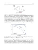
Assuming a delay cell variance of zero, i.e. no delay-stage mismatch, a plot of the integrated
spurious level due to the normalized in-lock error for different values of N was obtained using
Equation 9 and is shown in Fig. 14(a). These set of curves indicate the importance of reducing
the in-lock error to reduce the output spur level of the DLL based frequency multiplier. Note
also that for the same normalized in-lock error the spurious level increases with an increase
in the N value. The generality of the analysis presented above, permits also to estimate the
mean spurious level due to the possible mismatches in the VCDL. Fig. 14(b) shows a plot of
the mean estimated R
spur
against the normalized delay cell variation for different values of N,
assuming ΔT is equal to zero. As expected the higher the mismatch in the VCDL the higher
the spurious level the output of the frequency multiplier, indicating that the reduction of this
mismatch is equally important as the reduction of the DLL in-lock error.
Fig. 14. (a) Plot of the estimated integrated spurious level (N-1<k<N+1) against normalized
in-lock error for different values of N (b) Plot of the mean estimated integrated spurious level
against normalized delay cell variation for different values of N
3.4 DLL-based frequency synthesizer
The concept of using DLL-based frequency synthesizer architecture for UWB MBOA was
introduced in (Lee & Hsiao, 2006) and is shown in Fig. 15. Although the implementation
results showed that the architecture exhibits a sideband magnitude of -35.4 dBc (which is
within the specification), it considered only the generation of signals in the band group 1
(N = 13, 15, 17).
As discussed in Section 3.3, for the same normalised in-lock error and delay cell mismatch the
spurious level increases with an increase in the N value. Considering the generation of the
192
Ultra Wideband Communications: Novel Trends – System, Architecture and Implementation
Frequency Synthesizer Architectures for UWB MB-OFDM Alliance Application 13
Fig. 15. Proposed UWB MBOA Frequency Synthesizer Architecture in (Lee & Hsiao, 2006)
8.712 GHz signal which is the highest frequency in band group 6 one would require a value
of N = 33. Using the analysis presented in Section 3.3 it is possible to estimate the maximum
in-lock error and the maximum delay mismatch such that integrated spur level at the output
of the DLL frequency multiplier is less than -32 dBc. Note that one must keep in mind that
the
÷2 frequency divider at the output of the DLL improves the spur level at the output of the
DLL by 6.02 dB, such that R
spur
< -26 dBc. Assuming there is no mismatch in the delay stages,
the in-lock error ΔT needs to be less than (0.001073
÷ 528 MHz) = 2 ps for an input frequency
F
in
of 528 MHz as shown in Fig. 16. Since the in-lock error is generally determined by the PFD
and the CP, it is definitely not easy to design such circuits operating at 528 MHz. In fact the
in-lock error in the DLL frequency multiplier proposed in (Lee & Hsiao, 2006) is around 3.3 ps
which is definitely larger than the required value.
Fig. 16. Plot of the estimated spurious level against normalized in-lock error for N =33
Reducing the value of F
in
can ease the design of the PFD and the CP. This comes at the
cost of reducing the loop bandwidth of the DLL which is directed constrained by F
in
and so
increasing its settling time. An alternative architecture to the one proposed in (Lee & Hsiao,
2006) would be the one shown in Fig. 17 in which the three signals in each band group are
generated concurrently and fast switching between the signals in group is performed via the
multiplexer which can guarantee a switching time of less than 9.5 ns even if F
in
is not equal to
528 MHz.
Note that in this case F
in
is equal to 264 MHz such that a ÷2 frequency divider at the output is
not required. Note that in this case the in-lock error is still 2 ps as can be extracted from Fig. 16
but is definitely much easier to attain with a PFD and a CP operating at 264 MHz rather than
528 MHz. Further reduction of F
in
, to for instance 132 MHz would require a utilisation of
N = 66 thus degrading the spurious level such that the required in-lock error would still need
to be less than 2 ps.
193
Frequency Synthesizer Architectures for UWB MB-OFDM Alliance Application
14 Ultra Wideband Communications: Novel Trends
Fig. 17. Proposed DLL-based Frequency Synthesizer for BG 1, BG 3 and BG 6 signals
Fig. 18. Plot of the probability density of R
spur
for an output of 8.712 GHz from a DLL-based
FS with N = 33, F
in
= 264 MHz and σ
Tdcel l
/μ
Tdcel l
= 0.15%
In addition to the in-lock error, in an edge-combining DLL-based frequency synthesizer the
delay mismatch also degrades the spur level: assuming a perfectly locked DLL the variation
of the delay cell T
dcell
must be less than 90 fs for F
in
= 264 MHz (0.15%) to guarantee that
μ
Rs pur
+ 2σ
Rs pur
< -32 dBc as estimated using the analytic tool described in Section 3.3 (refer
to Fig. 18), where μ
Rs pur
is the mean and σ
Rs pur
is the standard deviation of R
spur
. Reduction
of the delay cell variation via transistor sizing as presented in (Casha et al., 2009b) is generally
limited to about 0.85% due to area considerations. Making use of a recirculating DLL surely
will complicate the design of the DLL due to the additional circuitry required (Gierkink, 2008).
Based on these considerations, a study on an UWB MBOA frequency synthesizer based on a
direct digital synthesizer was made due to the short comings of the DLL approach especially
for generating the high frequencies in the UWB MBOA spectrum.
4. CMOS Direct Digital Synthesizer for UWB MBOA
4.1 Concept of the Direct Digital Synthesizer (DDS)
Direct digital synthesis (DDS) provides a lot of interesting features for frequency synthesis.
It provides a fine frequency resolution suitable for state of the art digital communication
systems. Moreover, a digital architecture makes the DDS highly configurable and allows fast
settling time and fast frequency hopping performance. A conventional DDS consists of a
clocked phase accumulator, a phase to amplitude ROM, and a digital to analogue converter
(DAC) (Vankka, 2005). Depending on the slope of the phase accumulator, an output signal of a
194
Ultra Wideband Communications: Novel Trends – System, Architecture and Implementation
Frequency Synthesizer Architectures for UWB MB-OFDM Alliance Application 15
particular frequency is generated via the look-up table stored in the ROM and the DAC. DDS
generates spurious tones due to a phase to amplitude truncation. Increasing the resolution
of the ROM and the phase accumulator decreases the spurious level while on the other hand
increases the power dissipation and the ROM access time. Solutions have been proposed to
compress ROM capacity (Vankka (2005),Nicholas & Samueli (1991)).
Fig. 19. (a) Block diagram of a DDS (b) Concept of a 2-bit DDS withP=1
The DDS considered here is known as a phase-interpolation DDS (Badets & Belot (2003),
Nosaka et al. (2001), Chen & Chiang (2004)) which consists of an N-bit variable slope digital
integrator (adder and register), a 2-to-1 multiplexer (MUX), a digitally controlled phase
interpolator (PI) and a pulse generator. In this type of DDS no ROM is used. Its block diagram
representation is shown in Fig. 19(a) whilst the concept of a 2-bit DDS is depicted in Fig. 19(b)
to facilitate the explanation of the fundamental principle. On the arrival of every rising edge
from the input signal F
in
, the output of N-bit digital integrator increments according to the
assigned input control word P, such to control the digitally controlled phase interpolator to
generate a pulse via the pulse generator. Ideally this pulse lags the rising edge of F
in
by
an angle of 2π
R
2
N
radians, where N is the resolution of the digital integrator and R is the
instantaneous value of the register. Whenever an overflow occurs in the digital integrator, the
process is stopped for one cycle of the input signal, by changing the input control word value
from P to 0 and no pulse is generated.
F
out
=
2
N
2
N
+ P
F
in
where 1 ≤ P ≤ 2
N
−1 (10)
Through such mechanism, an output signal F
out
with a frequency given by Equation 10 is
generated. Equation 10 can be intuitively proven by noting that the process of the DDS
is repeated every 2
N
+ P input clock cycles, during which 2
N
pulses are generated at the
output. In Section 4.2 a formal proof of Equation 10 is presented. Such a concept can be
used to generate various sub frequencies from a main source without requiring the use of
multiple PLLs or analogue mixers. In practice, non-idealities in the phase interpolator cause
the generation of spurious tones at the output of the DDS: in Section 4.4.2 these non-idealities
are identified and ways how to reduce them are presented.
4.2 Transfer function of the DDS
Similarly to the case of the DLL, the transfer function of the DDS given by Equation 10 can be
derived by applying a Fourier analysis on its output. The DDS has a periodicity given by:
195
Frequency Synthesizer Architectures for UWB MB-OFDM Alliance Application
16 Ultra Wideband Communications: Novel Trends
T
DDS
= T
in
(2
N
+ P) (11)
where T
in
is the periodic time of the input signal, N is the resolution of the DDS and P is
the control word. Assuming there is some mechanism in the DDS to generate pulses of a
fixed duration and required phase shift from the input signal, it can be shown that the Fourier
content of the output is given by:
X
out
(kω
DDS
)=X
p
(kω
DDS
)
2
N
−1
∑
n=0
e
jkω
DDS
T
d
(n)
(12)
where X
p
is the Fourier transform of the pulse generated with no offset from the input signal,
i.e., the pulse generated when the digital accumulator value is equal to zero, T
d
is the delay
of the generated pulse and ω
DDS
is the angular frequency of the DDS. Ideally the phase
interpolator has a linear transfer function such that:
T
d
(n)=(T
in
+
P
2
N
T
in
)n = n
T
DDS
2
N
(13)
So the Fourier content of the DDS output signal can be written as:
X
out
(kω
DDS
)=X
p
(kω
DDS
)
2
N
−1
∑
n=0
e
j
2πnk
2
N
(14)
X
out
(kω
DDS
)=
2
N
X
p
(kω
DDS
) for k = 2
N
0 for k = 2
N
(15)
meaning that the output signal will have a frequency which is 2
N
times the periodic frequency
of the DDS, F
DDS
:
F
out
= 2
N
F
DDS
=
2
N
(2
N
+ P)T
in
=
2
N
(2
N
+ P)
F
in
(16)
Fig. 20. Position of spurs with respect to the desired output frequency in a practical DDS
In practice the transfer function of the phase interpolator is non-linear such that energy exists
in X
out
even for k = 2N. This means that the output spectrum will include spurious tones at
k
= 2N separated from each other by Equation 17 as shown in Fig. 20.
ΔF
spur
=
F
in
2
N
+ P
(17)
196
Ultra Wideband Communications: Novel Trends – System, Architecture and Implementation
Frequency Synthesizer Architectures for UWB MB-OFDM Alliance Application 17
4.3 Cascaded DDS
When a high resolution DDS is required, it is often possible to obtain the same function by
employing two cascaded low resolution DDS. A cascaded DDS topology, has the advantage
of facilitating the design at high frequency operation due to the need of low resolution circuit
blocks whilst the compensation of the phase interpolator non-ideality is more feasible. In this
case, the positioning of the spurious tones at the output of the cascaded DDS cannot be easily
derived as in the previous case. To simplify matters, two cascaded DDS can be represented
by the second DDS in the chain being fed by a jittery signal whose frequency and jitter are
defined by the first DDS in the cascaded chain. This is represented in Fig. 21(a).
Fig. 21. (a) Alternative representation of a cascaded DDS (b) Demonstration of the
positioning of the spurs of a DDS being fed by a jittery signal
If a DDS is injected by a jittery input signal y
in
represented by:
y
in
= A
i
sin(ω
i
t + A
j
sin ω
j
t) (18)
where ω
i
is the input frequency and ω
j
is the jitter frequency then the output will have
spurious tones separated from each other by the inverse of the least common multiple of
1/ f
j
and the periodicity of the DDS, i.e., (2
N
+ P)T
i
. A high level model of a DDS being fed
by a jittery signal was implemented in MATLAB to verify this result. Consider an example
with T
i
=1s,
ω
j
2π
= 0.25 Hz, N = 2, P = 1 and A
j
= 0.2 rad. The least common multiple of
4 s and (2
2
+ 1) is 20 s such that the expected spurious tones are separated by 0.05 Hz. The
simulation results confirm this as shown in Fig. 21(b). Now applying the above theory to the
cascaded DDS topology presented in Fig. 21(a) one can derive an expression describing the
positioning of the spurious tones in a cascaded DDS. In this case T
i
=(2
N
1
+ P
1
)T
in
/2
N
1
,
ω
j
= ω
in
/(2
N
1
+ P
1
), N = N
2
and P = P
2
, such that the output will have spurious tones
separated from each other by the inverse of the least common multiple of
(2
N
1
+ P
1
)T
in
and
the periodicity of the second stage
(2
N
2
+ P
2
)(2
N
1
+ P
1
)T
in
/2
N
1
. Since the latter is the least
common integer multiple of both terms then, for a cascaded DDS topology the spurious tones
at the output are located at:
F
spur
=
kF
in
2
N
1
(2
N
1
+ P
1
)(2
N
2
+ P
2
)
+
F
c
(19)
where F
c
is the expected cascaded DDS output frequency and k is an integer number.
197
Frequency Synthesizer Architectures for UWB MB-OFDM Alliance Application
18 Ultra Wideband Communications: Novel Trends
4.4 DDS-based frequency synthesizer
4.4.1 Architecture
The proposed architecture for the DDS-based frequency synthesizer is presented in Fig. 22.
As a proof of concept, the generation of the carrier signals in the sixth band group (BG 6)
of the UWB MBOA spectrum is considered. Since the frequency of the UWB MBOA signals
is a multiple of half the bandwidth (264 MHz) it is possible to generate the signals from a
reference
1
based on such frequency. For instance, the output signals in BG 6 are related to the
crystal frequency by:
44MHzx6x29 = 264 MHz x 29 = 7.656 GHz
44MHzx6x31 = 264 MHz x 31 = 8.184 GHz
44MHzx6x33 = 264 MHz x 33 = 8.712 GHz
Let us consider the synthesis of the 7.656 GHz signal and see how the architecture in Fig. 22
can generate it:
44MHz
×
6 ×29 × 31 ×33
8 ×128
×
1
4
×
2
5
2
5
+ 1
×
2
4
2
4
+ 15
×8 = 7.656GHz (20)
Fig. 22. Architecture of the DDS-based frequency synthesizer: a particular configuration of
the architecture which generates the required signals in BG6 of the UWB MBOA spectrum is
shown
The concept is to generate a reference frequency which is a multiple of 29x31x33 by means
of a PLL and then the 31x33 factor is effectively divided using the DDS structure in order
to generate the 7.656 GHz frequency. The other BG 6 frequencies are generated in a similar
way and concurrently with this one, without having to switch the frequency of the PLL or
requiring multiple PLLs. Note that a 128 divisor in the PLL feedback ratio together with the
fixed frequency dividers are required to cancel the frequency multiplication effect of the DDS
transfer function (refer to Equation 20).
A cascaded DDS topology rather than a single one is chosen, because as explained in
Section 4.3, the design of low resolution circuit blocks is easier considering the operation in the
gigahertz range and in addition the non ideality compensation is facilitated. Since in this feed
forward architecture, the three group signals are generated concurrently, it is possible to hop
from one frequency to another via multiplexing in an extremely short time (Alioto & Palumbo,
1
Implementation of high frequency Fractional-N PLLs is possible in submicron technologies such as
90nm and 65nm CMOS as demonstrated in (Ravi et al., 2004).
198
Ultra Wideband Communications: Novel Trends – System, Architecture and Implementation
Frequency Synthesizer Architectures for UWB MB-OFDM Alliance Application 19
2005). In addition, this architecture does not violate the phase coherency property, which is a
requirement of UWB MBOA frequency synthesizer (Batra et al., 2004a)
2
. The use of injection
locked frequency doublers (ILFD) permits the reduction of the DDS input frequency at the
cost of increasing the phase noise and spurious level gain in the synthesis path. This implies
that a careful design of the stages preceding the ILFD is fundamental, in order to limit their
phase noise and spurious level. A possible implementation of the ILFD is via injection-locked
ring oscillators which do not make use of integrated inductors thus limiting the utilised silicon
area (Badets et al., 2008).
Note that the signals in the other band groups can be generated by reconfiguring the
resolution of the DDS blocks and changing their P input, selecting between divide by-2 and
divide-by-4 frequency dividers in each path whilst changing the multiplication ratio of the
PLL accordingly. Note that the frequency hopping time from one band group to another is
not very demanding as in the case of the in-group frequency hoping (it is in the order of
milliseconds) making such an implementation a practical solution.
4.4.2 Spurious tones
The main sources of spurious tones in this architecture are the fractional-N reference PLL and
the DDS stages. It is imperative to reduce the spurs from the fractional-N PLL because they
will be increased and synthesized by passing through the chains of non-linear sub-blocks in
the system such as the cascaded DDS. Since this issue is already well discussed in literature
(Ravi et al. (2004), Kozak & Kale (2003)), this work focuses on the mechanisms in the DDS
stages leading to spurious tone generation and ways how to reduce them. The major spur
contributor in a DDS stage is the PI (Seong, 2006). A typically used PI, based on the Gilbert’s
multiplier cell is shown in Fig. 23.
Fig. 23. PI based on a Gilbert’s cell multiplier topology. Two such PI can be combined
together to cover the four phase quadrants (0
◦
< Θ < 360
◦
)
It consists of two complementary variable current bias circuits, implemented as DACs I
1
and I
2
which are controlled by a thermometer coded control word β, two differential pairs
driven by quadrature input signals, and two loads for each output node. Assuming perfectly
2
When the output in an UWB MBOA FS is hopping between the three possible frequencies in a particular
band group, it should always continue from the phase as if that frequency signal was never stopped.
199
Frequency Synthesizer Architectures for UWB MB-OFDM Alliance Application
20 Ultra Wideband Communications: Novel Trends
matched differential pairs it can be shown that the signal at the output node V
B
lags the V
I+
input by:
Θ
= −arctan(
I
2
I
1
)
1
η
(21)
where I
= I
1
+ I
2
is twice the constant current flowing through the load R
L
and η = 1 for large
signal operation and 1
≤ η ≤ 2 for small signal operation. As shown in Section 4.2, for the
DDS output to be free of spurious tones it is important that the phase transfer function of the
phase interpolator is linear. The transfer function of the phase interpolator can be linearised
by introducing systematic non-linearity in the current steering DACs. Considering DAC I
2
,
the amount of non linearity required to linearise the phase transfer function is given by:
I
m
I
2
=(
A
η
1 + A
η
×
2
N−2
β
−1) ×100% where A = tan(
βπ
2
N−1
) (22)
where N is the DDS resolution, β is the DAC control word and I
m
/I
2
is the percentage change
required in I
2
for a particular β value. Note that for β =0,2
N−3
and 2
N−2
, no compensation
is required. A similar process is applied to DAC I
1
, in this case a change opposite in sign to
that applied to I
2
. In practice since the non-linearity in the DACs is usually implemented via
the sizing of the transistors (Seong, 2006), it is not possible to exactly linearise the transfer
function as implied by Equation 22. In fact as a good layout practice, which is important
to limit the spurious tone energy due to DAC transistor mismatches, the transistors need
to be based on unit size transistor cells. Due to this discretisation in the transistor sizing,
the non-linear compensation as defined by Equation 22 cannot be exactly applied. Note also
that a quadrature error in the input signals or a mismatch in input transistors increases the
non-linearity in the phase transfer function which degrades the spurious level and makes
compensation more difficult too. In this architecture since the quadrature signals are derived
from the divide-by-2 or divide-by-4 frequency dividers, the signal quadrature error can be
kept quite low.
4.4.3 System level simulation
A system level model of the frequency synthesizer architecture was implemented using
MATLAB, to estimate its integrated spurious level, R
spur
, over a particular band (528 MHz).
A block diagram representation is shown in Fig. 24. This model assumes that the reference
frequency generated by the fractional-N PLL is free of spurious tones and that the architecture
consists of two cascaded DDS stages and a spurious tone gain stage of around 18 dB which
models the spurious level degradation due to the frequency multiplication effect of the ILFD.
The PI is modelled by the equations shown in Fig. 24. Since the PI of Fig. 23 can deliver phase
shifts in only one quadrant [0
◦
,90
◦
], the other quadrants are generated by having multiple PIs.
This is modelled by parameter λ, assuming that the PIs are identical. Both the non-linearity
of the phase transfer function and the variation of the current states (I
1
or I
2
) in the biasing
DACs due to transistor mismatches are considered. Note that each current state variation is
modelled by a standard normal distribution, X, with a mean zero and a standard deviation σ,
whose value is dependent on the current state
3
. Note that the pulse generator provides a pulse
of fixed duration on every rising edge of the PI signal. Using this model an estimate for spur
magnitude R
spur
for the signals in BG 6 was obtained for both an uncompensated PI (UPI)
3
The standard deviation of the current states σ =
β × σ
LSB
, where σ
LSB
is the standard deviation of
the least significant bit value.
200
Ultra Wideband Communications: Novel Trends – System, Architecture and Implementation
Frequency Synthesizer Architectures for UWB MB-OFDM Alliance Application 21
Fig. 24. System level model of the cascaded DDS topology implemented using MATLAB to
estimate the spurious tone energy at the output of the proposed frequency synthesizer,
where R is the value of N-bit register and λ is the quadrant number
and a compensated PI (CPI). The simulation results are given in Table 1. Note that, in this
case, no variation in the possible DAC current values was assumed (σ = 0). These estimations
show that by adequate non-linearity compensation the proposed architecture can generate
outputs which meet the spurious level specifications of UWB MBOA. Table 1 presents also the
separation of the spurious tones and the number of them captured in a given band confirming
the prediction given by Equation 19.
F
out
F
in
R
spur
R
spur
Spur No. of
(GHz) (GHz) (dBc) (dBc) Separation in-band
UPI CPI MHz spurs
7.656 1.91225 -25 -47 60 8
8.184 1.91225 -19 -44 64 8
8.712 3.82450 -42 -62 68 6
Table 1. Integrated R
spur
over a 528 MHz band for BG 6 signals
The compensation values for the two cascaded DDS were estimated using Equation 22 with
η = 1.35. These values were slightly rounded off to permit physical implementation via
transistor sizing as follows:
4-bit DDS: β=1: I
LBS
(1-0.065) β=3: I
LBS
(3+0.065)
5-bit DDS: β=1: I
LBS
(1-0.16) β=2: I
LBS
(2-0.16)
β=3: I
LBS
(3-0.08) β=5: I
LBS
(5+0.08)
β=6: I
LBS
(6+0.16) β=7: I
LBS
(7+0.16)
Fig. 25 shows a plot of the frequency content at the input of the three ILFD for both the
uncompensated (red plot) and the compensated case (black plot) of the 8.712 GHz signal
generation path. This plot shows substantial reduction of the magnitude of the spurious tones
in both the 528 MHz band of interest (blue plot) and the adjacent bands.
Another simulation was done this time considering a mismatch in the current states of the
DACs in a CPI. Table 2 presents the results of this Montecarlo simulation for the three signals
201
Frequency Synthesizer Architectures for UWB MB-OFDM Alliance Application
22 Ultra Wideband Communications: Novel Trends
Fig. 25. Frequency spectrum of the output of the cascaded DDS for the 8.712 GHz signal
generation path: (a) UPI in red (b) CPI in black (c) Band of interest in blue
in BG 6 over a sample of 300 DDS with σ
LSB
= 1% in the current steering DACs. This is
the maximum permissible DAC variation such that μ
Rs pur
+2σ
Rs pur
< -32 dBc for the three
signal generation paths, where μ
Rs pur
is the mean and σ
Rs pur
is the standard deviation of R
spur
.
Note that in the three cases μ
Rs pur
is higher than that given in Table 1 due to mismatch in
the current states of the DACs. Mismatch compensation of the DACs can be performed to
achieve mismatch levels as low as 1% as proposed in (Gagnon & MacEachern, 2008). Dynamic
element matching techniques can also be applied in the DAC design to reduce the effects of
mismatch (Henrik, 1998). Fig. 26 presents the results of the simulation for F
out
= 7.656 GHz
and σ
LSB
= 1%.
F
out
μ
Rs pur
σ
Rs pur
Maximum Minimum μ
Rs pur
+2σ
Rs pur
(GHz) (dBc) (dBc) R
spur
R
spur
(dBc)
(dBc) (dBc)
7.656 -42.58 5.58 -32.03 -59.35 -32.04
8.184 -37.81 1.73 -32.16 -43.24 -34.36
8.712 -57.28 3.31 -47.52 -62.79 -50.68
Table 2. Statistical simulation data of the variation of R
spur
for a DAC variation of 1% over a
sample of 300 cascaded DDS-based frequency synthesizers
These simulations indicate the importance of both linearising the phase transfer function of
the PI and reducing the variations of the DACs due to mismatches by good layout techniques
and adequate compensation (Gagnon & MacEachern, 2008). Note also that if it would be
possible to design a DDS which can be driven at higher frequencies than those proposed here,
the number of ILFD can be limited thus resulting in further reduction of the spurious level
at the output. In addition a higher F
in
implies also a larger separation between the spurs as
predicted by Equation 19, such that less spurs are captured in a given band although these
may still act as interferes to devices using the UWB MBOA on an adjacent band.
4.5 Design and simulation of circuit blocks
The critical blocks of this DDS, namely the digital accumulator, phase interpolator and the
pulse generator were designed in a 1.2 V 65-nm CMOS process. For the generation of BG 6
202
Ultra Wideband Communications: Novel Trends – System, Architecture and Implementation
Frequency Synthesizer Architectures for UWB MB-OFDM Alliance Application 23
Fig. 26. Plot of the probability density of R
spur
for an output of 7.656 GHz from a DDS-based
FS with compensated phase interpolator having current steering DACs with σ
LSB
=1%
signals, as shown in Fig. 22 the DDS stage being driven by the divide-by-2 frequency divider
is operating at the highest input frequency (around 4 GHz). Therefore the functionality of the
designed DDS building blocks as well as their impact on the FS performance was verified via
simulation at this frequency of operation.
4.5.1 Digital accumulator
The pipelined digital integrator considered in this study is shown in Fig. 27(a). The digital
integrator has the special feature to stop the integration process for one cycle after the
occurrence of an overflow. Due to the pipelining nature, this feature could not be implemented
by simply setting the P control word to zero, as shown in Fig. 19.
Fig. 27. (a) Block diagram of the 4-bit pipelined digital integrator (b) 1 bit integrator (DI) (c)
Pipeline DFF (P
DFF
) (d) Overflow DFF (O
DFF
)
In fact this could be only done by retaining the same state of the D-flip flops (DFFs) for one
cycle. This requires the implementation of a special type of DFF shown in Fig. 27(c) which
includes a 2-to-1 multiplexer (MUX) at its input being controlled by the integrator overflow
signal: on the arrival of a clock transition this DFF can either store the value of D
in
or hold
the previously stored value. In order to enable the integration after one idle cycle, a slightly
different DFF implementation is required for the overflow signal and is shown in Fig. 27(d): in
this case on the arrival of a clock transition, the DFF can either store the value of D
in
or store
the compliment of the previously stored value. Note that the overflow signal drives the DFFs
via a buffer. The DFFs were implemented using true-single phase clocking logic which allows
203
Frequency Synthesizer Architectures for UWB MB-OFDM Alliance Application
24 Ultra Wideband Communications: Novel Trends
high operating frequencies with lower power consumption than other techniques (Yuan &
Svensson, 1989). Fig. 28 shows a transient plot of the output (S
3−0
) and overflow (OF) signals
of the digital integrator with P = 15, being fed by a 4 GHz input frequency. The current
demand at typical process parameter corners, a temperature of 27
◦
C and a 1.2 V supply
voltage is 1.43 mA. The digital integrator can be operated at a maximum frequency of 4.5 GHz
under a slow corner condition at 105
◦
C with a supply voltage of 1.08 V.
Fig. 28. Transient plot of the 4-bit digital integrator for P=15 at an input frequency of 4 GHz
4.5.2 DDS controller
Fig. 29 shows the block diagram of a practical 4-bit DDS implementation. Since the differential
Gilbert cell based phase shifter is able to provide a phase shift in the range [0
◦
,90
◦
] and [180
◦
,
270
◦
] two such phase shifters are used in conjunction with a 4-to-1 current mode logic (CML)
multiplexer (Alioto & Palumbo, 2005) in order cover the four phase quadrants.
Fig. 29. Block diagram of a practical 4-bit DDS
The DDS controller has thus a two-fold task: according to the input word generated by the
digital accumulator S, the DDS controller must issue a control word Q, to select the required
phase quadrant via the 4-to-1 multiplexer and another two complementary control words β
and
¯
β to generate the required phase shift via the Gilbert cell based phase shifters. Note that
since the implemented phase shifter is based on thermometer coded DACs (see Section 4.5.3),
the DDS controller includes an encoder to translate the control words in the required format.
204
Ultra Wideband Communications: Novel Trends – System, Architecture and Implementation
Frequency Synthesizer Architectures for UWB MB-OFDM Alliance Application 25
4.5.3 Phase interpolator
As explained above, the phase interpolator was implemented using two phase shifters shown
in Fig. 23 together with a 4-to-1 CML multiplexer (Alioto & Palumbo, 2005) to cover the four
phase quadrants (Fig. 29). In order to minimise the level spurious tones, the critical section of
the phase interpolator is the non-linear compensation of the current steering DACs I
1
and I
2
.
Fig. 30. Differential thermometer decoded DAC with non-linear compensated transistors
The current steering in the PI cell is achieved via 5-state differential thermometer coded DACs,
shown in Fig. 30. This DAC design permits the operation at high frequencies since the current
sources are never switched off and in addition two complementary DACs are implemented
in a single one, thus reducing silicon area. Due to the thermometer nature, the required
non-linearity in the DACs is easily introduced by non-uniform sizing of the transistors (M
1−4
).
Table 3 shows how non-uniform sizing of the M
1−4
can be applied. It can be easily seen that
this is the compensation discussed in Section 4.4.2 for a four bit DDS.
M1 M2 M3 M4
Uncompensated W/L X X X X
Compensated W/L X-ΔX X+ΔX X+ΔX X-ΔX
Table 3. Non-uniform sizing of transistors in current steering DACs
Using Equation 22 the compensation required for a four bit DDS was estimated to be Δ = 0.065.
It is important to note that the aspect ratio of all transistors must be composed of an integer
number of common unit cells to permit interdigitation in the layout. This is essential to limit
mismatch between the transistors and thus limiting mismatch in the DACs which also incur
degradation in the spurious tones at the output of the DDS. This implies that Δ
=
n
1
n
2
must be
a rational fractional with n
1
and n
2
being either both odd integers or both even integers. In
this case the closest integers to 0.065 are n
1
= 1 and n
2
= 15 such that Δ = 0.067. Taking the
uncompensated transistor gate channel width to be 30 μm, the sizes of the DAC transistors
shown in Fig. 30 were determined, with 4 μm being the gate width of the common unit cell.
Table 4 shows the difference between the theoretical (given by Equation 21) and the practical
compensated phase shift response of the PI cell of Fig. 30 for the 5 current state positions. At
an input frequency of 4 GHz a constant 25
◦
phase shift is noted due to the finite bandwidth
of the PI cell. This does not affect the functionality of the DDS since it is almost uniform
at each current state position. As regards the power consumption, post layout simulations
205
Frequency Synthesizer Architectures for UWB MB-OFDM Alliance Application
26 Ultra Wideband Communications: Novel Trends
β
3
β
2
β
1
β
0
I
1
(mA) I
2
(mA) Theoretical Actual Phase Actual Phase
Phase(
◦
) 1 GHz(
◦
) 4 GHz(
◦
)
1111 1.69e-5 2.71 -89.99 -89.95 -114.95
0111 0.641 2.14 -67.76 -67.23 -92.23
0011 1.41 1.41 -45.00 -44.87 -69.87
0001 2.14 0.641 -22.24 -21.39 -46.39
0000 2.72 8.20e-5 -0.03 -4.46e-2 -25.05
Table 4. Theoretical and practical compensated phase shift response of the PI cell
indicate that the PI cell demands 2.78 mA whilst the 4-to-1 MUX demands 2.86 mA at 27
◦
C.
Fig. 31 shows a plot of the relative spur content of the compensated phase interpolator output
for both the transistor level simulations and the MATLAB high level model simulations for
different values of P in which an input frequency of 4 GHz was considered.
Fig. 31. Relative spur levels at the output of phase interpolator
As can be noted from Fig. 31, the simulation results match the predicted results. In addition
one can note that the relative spur levels at the output of the PI are high for the given
application. In fact this is caused due to the number of discontinuities in the output waveform
which "hide" the phase shift information. The important information in the output signal
of the phase interpolator is the phase shift from the input signal. This can be extracted via
a technique in which a square wave pulse signal is generated (see Fig. 32(a)). The rising
edges of this square wave signal are used to trigger pulses of fixed duration via a one-shot
multivibrator discussed in Section 4.5.4. For clarity, Fig. 32(b) shows the principle of this
technique for a 2-bit DDS. Note that the discontinuities in the output of the PI are highlighted.
Fig. 33 shows a comparison between the frequency spectrum of the output of the phase
interpolator and the output of the pulse generator of a 4-bit DDS with P = 15 obtained via
MATLAB simulations. It shows the effectiveness of the algorithm to eliminate spurs due
to discontinuities in the output of the phase interpolator. Note that the PI is compensated
accordingly to have a linear transfer function.
206
Ultra Wideband Communications: Novel Trends – System, Architecture and Implementation
Frequency Synthesizer Architectures for UWB MB-OFDM Alliance Application 27
Fig. 32. (a) Block diagram of the technique to extract phase information (b) Concept of the
technique for a 2-bit DDS with P=3
Fig. 33. Comparison between the frequency spectrum of PI and the Pulse Generator
4.5.4 Pulse generator
Fig. 34(a) shows the circuit diagram of the pulse generator used to generate a pulse signal of
constant pulse-width at every rising edge of the signal generated by the wave shaping circuit.
It is based on the one-shot multivibrator circuit proposed in (Lockwoodm, 1976) with the
difference that it is based on CMOS inverters rather than NMOS inverters to limit the power
consumption and includes buffering at both the input and the output stages. To permit
reliable operation of the one-shot multivibrator at high frequencies, the implementation does
not include any regenerative feedback mechanisms. This was possible since the pulse width
required can be made to be smaller than the pulse width of the incoming signal.
Fig. 34(b) presents the transient response of the pulse generator for an applied pulse signal of
around 2 GHz generating a pulse of 70 ps whilst demanding an average current of 273 μA.
When the input signal V
in
increases, node voltage V
a
follows it, since it is a buffered version of
V
in
. As a consequence since the voltage on capacitor C cannot change instantaneously, node
voltage V
b
increases too making the output go high. The capacitor starts charging up via
transistors M
4
and M
3
, where the latter acts as a current source. Since V
a
is fixed at around
1.2 V, V
b
starts going down to permit the capacitor to charge up. When V
b
goes below the
207
Frequency Synthesizer Architectures for UWB MB-OFDM Alliance Application
28 Ultra Wideband Communications: Novel Trends
Fig. 34. (a) Feed forward CMOS one-shot multivibrator (b) Transient response of the pulse
generator for an input frequency of 2 GHz
threshold of the output buffer the output goes low again. The pulse duration thus depends
on the size of the capacitor and the current mirrored in M
3
.
4.5.5 Performance summary
The sections above presented the design and simulation of the main circuit blocks used in a
DDS to be driven by an input frequency of around 4 GHz. Table 5 presents a summary of
the current demand of these circuit blocks. Note that the DDS used to generate the 8.712 GHz
signal in BG 6 was chosen to study the maximum current demand in the frequency synthesizer
architecture. The other DDS in the frequency synthesizer architecture presented in Fig. 22 can
be designed with a lower current demand whilst achieving the same transient performance
since they are driven at a lower input frequency.
Block Description Current Demand
4-bit digital accumulator 1.43 mA
Gilbert Cell Based Phase Shifters 2.78 mA (x2)
4x1 CML Multiplexer 2.86 mA
Pulse Generator 273 μA
Table 5. Summary of the current demand of the main DDS circuit blocks
Simulation results show that a 4-bit DDS designed around the presented digital integrator (at
P = 15) and the 4-quadrant PI, has an integrated output spurious level of approximately of
-60 dBc over a 528 MHz band. The frequency content of the PI output and the pulse generator
output of the DDS are shown in Fig. 35.
Since the ILFD degrades the spurious level by 18 dB, assuming the second cascaded DDS has
similar characteristics as the first DDS stage, an integrated spurious level of approximately
-42 dBc can be estimated at the output for the 8.712 GHz signal. The difference between
the practical simulations shown in Fig. 35 and the system level simulations comes from the
jitter limitations in the practical phase extraction technique, the one shot pulse generator
(Lockwoodm, 1976) and from second order effects such as the channel length modulation
of the DAC transistors which introduce additional and unaccounted-for non-linearities in the
phase interpolator transfer function. The estimated spur level is still within the specifications
of the UWB MBOA.
208
Ultra Wideband Communications: Novel Trends – System, Architecture and Implementation
Frequency Synthesizer Architectures for UWB MB-OFDM Alliance Application 29
Fig. 35. Frequency content of the PI output and the pulse generator output of the DDS
5. Conclusion
The first part of this chapter discussed and compared the current state of the art in frequency
synthesis for UWB MBOA applications; in particular frequency synthesizers based on single
side band frequency mixing were tackled. In the second part, the chapter presented a study
on novel frequency synthesis architectures proposed as low silicon area alternatives to state
of the art solutions: one is based on DLLs whilst the other is based on the phase-interpolation
DDS. In particular, an investigation of the spurious tones in such architectures was presented
and ways how to reduce them are discussed. These architectures can enable the reduction of
the required silicon area by limiting the number of required PLLs and the removal of analogue
mixers from the architectures.
Based on this study, conclusions can be drawn indicating the advantages and disadvantages
of each architecture. The main advantage of the DDS-based FS is that being a feed-forward
architecture, the design does not have to take care of stability issues in the three respective
signal generation paths, as in the case of the DLL based FS. This is an important issue
especially during reconfiguration of the system to generate signals of different frequencies
in the various bands. The DDS architecture can be seen as a more modular architecture
since the main synthesizing block is the same in the three respective signal generation paths.
The DLL-based FS requires an input reference which is much lower than that of the other
architecture, thus facilitating its generation. In addition, the DLL-based FS does not make use
of ILFD as in the DDS-based FS, which degrade both the phase noise and spurious tone level
at the output of the synthesizer. The number of utilised ILFD can be reduced if the DDS can
be operated at a high input frequency.
Although the DDS architecture generates more spurs in a given band than the DLL
architecture, they are small in magnitude especially those in the vicinity of the desired output
frequency. In the DLL architecture the spurs adjacent to the required output signal contain
the highest amount of energy and are therefore more prone to have a degrading effect on
the integrated spurious level in the chosen band of operation as well as adjacent bands. The
analyses have shown that spur compensation in the DLL via in-lock error and delay stage
mismatch minimisation are generally much more difficult than spur compensation in the DDS
architecture. This is particular true when the DLL is used to generate high frequency signals
such as those in BG 6 which require a loop in lock error of less than 2 ps and a mismatch
in the delay cell of less than 80 fs for an input frequency of 264 MHz. To eliminate the
209
Frequency Synthesizer Architectures for UWB MB-OFDM Alliance Application
30 Ultra Wideband Communications: Novel Trends
problems associated with delay mismatches one needs to use a recirculating type DLL at the
expense of a more complex feedback loop design. Spurious tones minimisation via non-linear
phase interpolator compensation and mismatch compensation in the DACs is facilitated in
the DDS architecture since low resolution cascaded DDS are used. In light of spurious tone
minimisation, the layout of the main synthesizing blocks can prove to be easier for the DDS
than for the DLL.
6. References
Alioto M. & Palumbo G. (2005). Model and design of Bipolar and MOS current-mode logic:
CML, ECL and SCL digital circuits, Kluwer Academic Publishers - Springer, ISBN:
1402028784.
Badets, F. & Belot D. (2003). A 100 MHz DDS with synchronous oscillator-based
phase interpolator, International Solid-State Circuits Conference (ISSCC), pp. 410-503,
February 2003.
Badets, F. et al. (2008). Injection Locked CMOS Buffer Dedicated to NanoMagnetic Based
Voltage Controlled Oscillator, Proceedings of the ICECS 2008, pp. 190-193, Malta,
August 2008, St. Julian’s.
Batra, A. et al. (2004a). Multi-Band OFDM Physical Layer Proposal for IEEE 802.15 Task Group 3a,
Multi-Band OFDM Alliance SIG.
Batra, A. et al. (2004b). Design of a multiband OFDM system for realistic UWB channel
environments, IEEE Transactions on Microwave Theory and Technology, Vol., 52,
September 2004, pp. 2123-2138, ISSN: 0018-9480.
Casha, O.; Grech, I. & Badets, F. (2009a). CMOS Phase-Interpolation DDS for an UWB
MB-OFDM Alliance Application, Proceedings of the 5th PRIME Conference, pp. 200-203,
Ireland, July 2009, Cork.
Casha, O. et al. (2009b). Analysis of the Spur Characteristics of Edge Combining DLL-based
Frequency Multipliers, IEEE Transactions on Circuits and Systems-II: Express Briefs, Vol.,
56, February 2009, pp. 132-136, ISSN: 1549-7747.
Chang, J. et al. (2009). A Single-PLL UWB Frequency Synthesizer Using Multiphase Coupled
Ring Oscillator and Current-Reused Multiplier, IEEE Transactions on Circuits and
Systems II: Express Briefs, Vol., 56, February 2009, pp. 107-111, ISSN: 1549-7747.
Chen, H.C. & Chiang, J.S. (2004). A Low-Jitter Phase-Interpolation DDS Using Dual-Slope
Integration, IEICE Electronics Express, Vol., 1, September 2004, pp. 333-338, ISSN:
1349-2543.
Chien, G. & Gray, P.R. (2000). A 900-MHz Local oscillator using a DLL-based Frequency
Multiplier Technique for PCS Applications, IEEE Journal of Solid-State Circuits, Vol.,
35, December 2000, pp. 1996-1999, ISSN: 0018-9200.
Gagnon, G. & MacEachern, L. (2008). Digital compensation of DAC mismatches in multibit
delta-sigma ADCs, Electronics Letters, Vol., 44, June 2008, pp. 721-722, ISSN:
0013-5194.
Gierkink, S. (2008). An 800 MHz -122dBc/Hz-at-200kHz clock multiplier based on a
combination of PLL and recirculating DLL, Proc. 2008 IEEE International Solid-State
Circuits Conference, pp. 454-455, ISSN: 0193-6530.
Henrik, T.J. (1998). A Low-Complexity Dynamic Element Matching DAC for Direct Digital
Synthesis, IEEE Transactions on Circuits and Systems-II: Analog and Digital Signal
Processing, Vol., 45, January 1998, pp. 13-27, ISSN: 1057-7130.
210
Ultra Wideband Communications: Novel Trends – System, Architecture and Implementation
Frequency Synthesizer Architectures for UWB MB-OFDM Alliance Application 31
Ismail, A. & Abidi, A. (2005a). A 3.1 to 8.2 GHz direct conversion receiver for MB-OFDM UWB
communications, Proceedings of the IEEE International Solid-State Circuits Conference
Digest of Technical Papers, pp. 208-209, ISSN: 0193-6530.
Ismail, A. & Abidi, A. (2005b). A 3.1- to 8.2-GHz zero-IF receiver and direct frequency
synthesizer in 0.18- μm SiGe BiCMOS for mode-2 MB-OFDM UWB communication,
IEEE Journal of Solid-State Circuits, Vol., 40, December 2005, pp. 2573-2582, ISSN:
0018-9200.
Jiang, X. et al. (2010). A single-PLL dual-PPF synthesizer for Mode-1 MB-OFDM UWB
communication, Journal of Analog Integrated Circuits and Signal Processing, Vol., 62,
2010, pp. 291-299.
Kim, C. et al. (2007). A CMOS Frequency Synthesizer Block for MB-OFDM UWB Systems,
ETRI Journal, Vol., 29, April 2007, pp. 437-444, ISSN: 1225-6463.
Kozak, M. & Kale, I. (2003). Oversampled Delta-Sigma Modulators, Kluwer Academic Publishers,
Springer, ISBN: 1402074204, Boston.
Lee, J. & Chiu, D.W. (2005). A 7-band 3-8 GHz frequency synthesizer with 1 ns band-switching
time in 0.18μm CMOS technology, Proceedings of the IEEE International Solid-State
Circuits Conference Dig. Technical Papers, pp. 204-205, 2005, ISSN: 0193-6530.
Lee, T.C. & Hsiao, K.J. (2005). A DLL-based Frequency Multiplier for MBOA-UWB System,
Proceedings of 2005 Symposium on VLSI Circuits Digest of Technical Papers, pp. 42-45,
July 2005.
Lee, T.C. & Hsiao, K.J. (2006). The Design and Analysis of a DLL-Based Frequency Synthesizer
for UWB Application, IEEE Journal of Solid-State Circuits, Vol., 41, June 2006, pp.
1996-1999, ISSN: 0018-9200.
Lee, T.C. & Huang, Y.C. (2006). The design and analysis of a Miller-divider-based clock
generator for MBOA-UWB application, IEEE Journal of Solid-State Circuits, Vol., 41,
June 2006, pp. 1253-1261, ISSN: 0018-9200.
Lee, J. (2006). A 3-to-8-GHz fast-hopping frequency synthesizer in 0.18-μm CMOS technology,
IEEE Journal of Solid-State Circuits, Vol., 41, March 2006, pp. 566-573, ISSN: 0018-9200.
Leenaerts, D.M.W. (2005). A SiGe BiCMOS 1 ns fast hopping frequency synthesizer for UWB
radio, Proceedings of the IEEE International Solid-State Circuits Conference Digest of
Technical Papers, pp. 202-203, 2005, ISSN: 0193-6530.
Leenaerts, D. M. W. (2006). Transceiver design for multiband OFDM UWB, EURASIP Journal
of Wireless Communication Networks, 2006, pp. 1-8.
Liang, C.F. et al. (2006). A 14-band frequency synthesizer for MB-OFDM UWB application,
Proceedings of the IEEE Solid-State Circuits Conference, pp. 428-437, 2006, ISSN:
0193-6530.
Lin, C.C. & Wang, C.K. (2005a). Subharmonic direct frequency synthesizer or mode-1
MB-OFDM UWB system, Proceedings of the Symposium on VLSI Circuits Digest of
Technical Papers, pp. 38-41, 2005, ISBN: 4-900784-01-X.
Lin, C.C. & Wang, C.K. (2005b). A regenerative semi-dynamic frequency divider for mode-1
MB-OFDM UWB hopping carrier generation, Proceedings of the IEEE International
Solid-State Circuits Conference Digest of. Technical Papers, pp. 206-207, 2005, ISSN:
0193-6530.
Lockwoodm, G.C. (1976). One Shot Multivibrator Circuit, US Patent 3996482, December 1976.
Lu, T.Y. & Chen, W.Z. (2008). A 3-to-10 GHz 14-band CMOS frequency synthesizer with spurs
reduction for MB OFDM UWB system, Proceedings of the IEEE Solid-State Circuits
Conference, pp. 126-601, 2005, ISSN: 0193-6530.
211
Frequency Synthesizer Architectures for UWB MB-OFDM Alliance Application
32 Ultra Wideband Communications: Novel Trends
Mishra, C. et al. (2005). Frequency planning and synthesizer architectures for multiband
OFDM UWB radios, IEEE Transactions on Microwave Theory and Technology, Vol., 53,
December 2005, pp. 3744-3756, ISSN: 0018-9480.
Nicholas, H.T. & Samueli, H. (2005). A 150-MHz Direct Digital Frequency Synthesizer in
1.25-μm CMOS with -90-dBc Spurious Performance, International Journal of Solid-State
Circuits, Vol., 26, December 1991, pp. 1959-1969, ISSN: 0018-9200.
Nosaka, H. et al. (2001). A Low-Power Direct Digital Synthesizer Using a Self-Adjusting
Phase-Interpolation Technique, International Journal of Solid-State Circuits, Vol., 36,
August 2001, pp. 1281-1285, ISSN: 0018-9200.
Pufeng, C. et al. (2010). A 6-9 GHz 5-band CMOS synthesizer for MB-OFDM UWB, Journal of
Semiconductors, Vol., 31, July 2010, ISSN: 1674-4926.
Ravi, A. et al. (2004). 8 GHz, 20mW, fast locking, fractional-N frequency synthesizer with
optimized 3rd order, 3/5 bit IIR and 3rd order 3-bit-FIR noise shapers in 90nm CMOS,
CICC 2004, pp. 625-628, October 2004.
Razavi, B. et al. (2005). A UWB CMOS Transceiver, IEEE Journal of Solid-State Circuits, Vol., 40,
December 2005, pp. 2555-2562, ISSN: 0018-9200.
Roovers, R. et al. (2005). An Interference-Robust Receiver for Ultra-Wideband Radio in SiGe
BiCMOS Technology, IEEE Journal of Solid-State Circuits, Vol., 40, December 2005, pp.
2563-2572, ISSN: 0018-9200.
Sandner, C. et al. (2006). A WiMedia/MBOA-Compliant CMOS RF Transceiver for UWB, IEEE
Journal of Solid-State Circuits, Vol., 41, December 2006, pp. 2787-2794, ISSN: 0018-9200.
Seong, C.K. (2006). A 1.25 Gb/s digitally-controlled dual loop clock and data recovery circuit with
enhanced phase resolution, M.Sc. Thesis, Graduate School of Yonsei University.
Tanaka, A. et al. (2006). A 1.1V 3.1-9.5 GHz MB-OFDM UWB transceiver in 90 nm CMOS,
Proceedings of the IEEE International Solid-State Circuits Conference Digest of. Technical
Papers, pp. 120-121, 2006, ISSN: 0193-6530.
Valdes-Garcia, A. et al. (2006). An 11-Band 3.4 to 10.3 GHz MB-OFDM UWB receiver in 0.25 μm
SiGe BiCMOS, Proceedings of the Symposium on VLSI Circuits Technical Digest Papers,
pp. 254-255, 2006, ISBN: 1-4244-0006-6.
Valdes-Garcia, A. et al. (2007). An 11-Band 3-10 GHz Receiver in SiGe BiCMOS for Multiband
OFDM UWB Communication, IEEE Journal of Solid-State Circuits, Vol., 42, April 2007,
pp. 935-948, ISSN: 0018-9200.
Van de Beek, R.C.H. et al. (2006). A Fast-Hopping Single-PLL 3-Band MB-OFDM UWB
Synthesizer, IEEE Journal of Solid-State Circuits, Vol., 41, July 2006, pp. 1522-1529,
ISSN: 0018-9200.
Vankka, J. (2005). Digital Synthesizers and Transmitters for Software Radio, Springer, ISBN:
1402031947, Netherlands.
Yuan, L. & Svensson, C. (1989). A 1.5 V 3.1 GHz-8 GHz CMOS Synthesizer for 9-Band
MB-OFDM UWB Transceivers, IEEE Journal of Solid-State Circuits, Vol., 24, January
1989, pp. 62-70, ISSN: 0018-9200.
Zheng, H. & Luong, H.C. (2007). A 1.5 V 3.1 GHz-8 GHz CMOS Synthesizer for 9-Band
MB-OFDM UWB Transceivers, IEEE Journal of Solid-State Circuits, Vol., 42, June 2007,
pp. 1250-1260, ISSN: 0018-9200.
Zhuang, J. et al. (2004). Noise, Spur Characteristics and in-lock error reduction of DLL-based
frequency Synthesizers, Proc. International Conference on Communications, Circuits and
Systems, pp. 1443-1446, 2004.
212
Ultra Wideband Communications: Novel Trends – System, Architecture and Implementation
11
Ultra-Wideband GaN Power Amplifiers - From
Innovative Technology to Standard Products
Andrey Kistchinsky
Microwave Systems JSC
Russia
1. Introduction
A number of the modern electronic systems applications require generation, processing,
amplification, and emission of signals that have a continuous broadband spectrum or
modulated signals with a relatively narrow spectrum whose frequency may change in broad
ranges. The first group of applications may include UWB systems of short distance data
transmission, radar systems with UWB signals of different kinds (pulse, multi-frequency,
or quasi-noise), RFID-systems, and a number of others. The second group includes
electronic warfare (EW) systems, EMC-testing systems, as well as universal measuring
and testing equipment.
Usually, signals with fractional bandwidth over 20% of band center or more than 500 MHz
of absolute bandwidth are referred to UWB signals. As applied to the signal-processing
devices, in particular, to amplifiers, the interpretation of the term UWB is somewhat
different. Depending on the relative bandwidth the amplifiers are usually divided into the
following kinds: narrowband (frequency coverage - relation of the upper working frequency
to the lower working frequency (W) is less than 1.2:1); wideband (W from 1.2:1 to 2:1), and
ultra-wideband ones (W greater than 2:1). In the present article we shall speak about
technologies of microwave ultra-wideband power amplifiers.
The main parameters determining the possibility of using an power amplifier in a definite
electronic system are as follows: a working frequency bandwidth (ΔF), the output power
with the given criteria of distortion (Po), and the efficiency of transformation DC source
power into the output power (DE). With the increase of the frequency coverage W the
achieved DE is significantly lowered. Some typical dependence of DE on W, built for typical
microwave transistor power amplifiers, is shown in Fig.1.
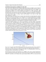
The highest DE values (up to 70-80%) are realized due to different special circuits, named
Harmonic Reaction Amplifiers (Colantonio et al., 2009). In these circuits a special
combination of transistor source and load impedances and special biasing allows to
achieve the forms of drain current and voltage close to the switching form which results
in minimal losses of DC source energy. However, the frequency coverage W, in which
these combinations may be realized, is usually limited by 1.1:1 to 1.2:1 values. Amplifiers
with the frequency coverage up to 1.5:1 may be built by classical A/AB biasing schemes
with multi-contour reactive input and output matching circuits. The forms of currents
and voltages in such schemes are close to sinusoidal ones while the DE is limited by the
values of 40-50%.