Frontiers in Guided Wave Optics and Optoelectronics Part 8 pdf
Bạn đang xem bản rút gọn của tài liệu. Xem và tải ngay bản đầy đủ của tài liệu tại đây (3.68 MB, 40 trang )
All-Optical Wavelength-Selective Switch by Intensity Control in Cascaded Interferometers
265
3.2 Switch B
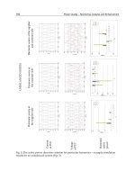
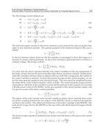
The switching operation with switch B is also verified by FD-BPM simulation. The model
used in the simulation is shown in Fig. 9. The total length of the switch is L=8.85 mm.
Raman
amp.
α
I
A
I
B
O
A
O
B
3dB
coupler
L
c
L
s
L
p
L
D
d
W
z
x
Fig. 9. Two-dimensional model of switch B for FD-BPM simulation.
-20 1
10log|E|
2
A
in
B
out
A
out
[dB]
(a)
1
α
=
- 10 15. 484
A
in
B
out
A
out
10log|E|
2
[dB]
(b)
3.383
α
=
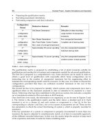
Fig. 10. Distribution of optical fields with two different switching conditions in swith B.
The switching operation at λ=1550 nm is confirmed as shown in Fig. 10. Although the output
intensities from output port O
A
and O
B
are different, switching is successfully simulated.
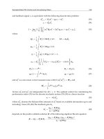
The wavelength dependence is shown in Fig. 11. At the designed wavelength
λ=1550nm, the
switching extinction ratio is larger than 25 dB. The wavelength range to achieve the
extinction ratio larger than 20 dB is approximately 30 nm, though the 10-dB extinction ration
is obtained over 80 nm.
Frontiers in Guided Wave Optics and Optoelectronics
266
-30
-25
-20
-15
-10
-5
0
5
1500 1520 1540 1560 1580 1600
Wavelength (nm)
Relative output intensity (dB)
A
out
B
out
(a)
1
α
=
-20
-15
-10
-5
0
5
10
15
20
25
1500 1520 1540 1560 1580 1600
Wavelength (nm)
Relative output intensity (dB)
A
out
B
out
(b)
3.383
α
=
Fig. 11. Wavelength dependence of switched outputs for the switch B designed at
wavelength
λ=1550nm.
4. Improvement of wavelength dependency
Waveguide-type Raman amplifiers do not depend on wavelength bands to be used because
stimulated Raman scattering which is the base effect of Raman amplification can occur at
any wavelength bands. Meanwhile, 3dB couplers have wavelength dependency in general,
that is, the function of dividing an incident optical wave into two waves at the rate of 50:50
is available at some particular wavelength bands. The main cause of the wavelength
dependency is the wavelength dependence of the coupling coefficient κ in eq.(1). For
improving the characteristics of wavelength dependency of the switch and utilizing it at any
All-Optical Wavelength-Selective Switch by Intensity Control in Cascaded Interferometers
267
wavelength bands, wavelength-independent (or wavelength-flattened) optical couplers
should be employed. Fiber-type wavelength-independent couplers, that can be used for
50:50 of the dividing rate at wavelength bands such as 1550 nm
± 40 nm and 1310 nm ± 40
nm, have already been on the market. However, waveguide-type wavelength-independent
couplers have advantage from the viewpoint of integrating the switch elements.
An alternative for improving wavelength dependence is to replace the directional couplers
by asymmetric X-junction couplers (Izutsu et al., 1982; Burns & Milton, 1980; Hiura et al.,
2007). The asymmetric X-junction coupler has basically no dependence on wavelength and
helps to improve the wavelength dependency of the proposed switch (Kishikawa et al.,
2009a; Kishikawa et al., 2009b).
5. Another issue in implementation
Phase shift of the signal pulse experienced in the waveguide-type Raman amplifiers should
be discussed because it can impact the operation of the switch. The phase shift is induced
from refractive index change caused by self-phase modulation (SPM), cross-phase
modulation (XPM), free carriers generated from two-photon absorption (TPA) (Roy et al.,
2009), and temperature change. Although the structure of the switch becomes more
complex, the effect of SPM and TPA-induced free carriers can be cancelled by installing the
same nonlinear waveguides as those of the waveguide-type Raman amplifiers into counter
arms of the Mach-Zehnder interferometers of the switch. The influence of XPM and
temperature change involved with high power pump injection can also be suppressed by
injecting pump waves, having the same power and different wavelengths that do not
amplify the signal pulse, into the counterpart nonlinear waveguides.
6. Conclusion
We proposed a novel all-optical wavelength-selective switching having potential of a few tens
of picosecond or faster operating speed. We discussed the theory and the simulation results of
the switching operation and the characteristics. Moreover, the dynamic range over 25dB was
also obtained from the simulation results of the switch. This characteristics can be wavelength-
selective switching operation. More detailed analysis and simulation taking the nonlinearity of
Raman amplifiers into account are required to confirm the operation with actual devices.
Although the principle and the fundamental verification were performed with the switches
consisting of directional couplers, the idea can be similarly applied to switches consisting of
other components such as asymmetric X-junction couplers to increase the wavelength range.
8. References
Doran, N. J. & Wood, D. (1988). Nonlinear-Optic Loop Mirror, Optics Lett., vol.13, no.1,
pp.56-58, Jan. 1988.
Burns, W. K. & Milton, A. F. (1980). An Analytic Solution for Mode Coupling in Optical
Waveguide Branches, IEEE J. Quantum Electron., vol.QE-16, no.4, pp.446-454, Apr.
1980.
Goh, T., Kitoh, T., Kohtoku, M., Ishii, M., Mizuno, T. & Kaneko, A. (2008). Port Scalable PLC-
Based Wavelength Selective Switch with Low Extinction Loss for Multi-Degree
ROADM/WXC, The Optical Fiber Communication Conference and the National
Fiber Optic Engineers Conference (OFC/NFOEC2008), San Diego, OWC6, Mar. 2008.
Frontiers in Guided Wave Optics and Optoelectronics
268
Goto, N & Miyazaki, Y. (1990). Integrated Optical Multi-/Demultiplexer Using Acoustooptic
Effect for Multiwavelength Optical Communications, IEEE J. on Selected Areas in
Commun., vol.8, no.6, pp.1160-1168, Aug. 1990.
Hadley, G. R. (1992). Wide-Angle Beam Propagation Using Pade Approximant Operators,
Opt. Lett., vol.17, no.20, pp.1426-1428, Oct. 1992.
Hiura, H., Narita, J. & Goto, N. (2007). Optical Label Recognition Using Tree-Structure Self-
Routing Circuits Consisting of Asymmetric X-junction, IEICE Trans. Commun.,
vol.E90-C, no.12, pp.2270-2277, Dec. 2007.
Izutsu, M., Enokihara, A. & Sueta, T. (1982). Optical-Waveguide Hybrid Coupler, Opt. Lett.,
vol.7, no.11, pp.549-551, Nov. 1982.
Kishikawa, H. & Goto, N. (2005). Proposal of All-Optical Wavelength-Selective Switching
Using Waveguide-Type Raman Amplifiers and 3dB Couplers, J. Lightwave
Technol., vol.23, no.4, pp.1631-1636, Apr. 2005.
Kishikawa, H. & Goto, N. (2006). Switching Characteristics of All-Optical Wavelength-
Selective Switch Using Waveguide-Type Raman Amplifiers and 3-dB Couplers,
IEICE Trans. Electron., vol.E89-C, no.7, pp.1108-1111, July 2006.
Kishikawa, H. & Goto, N. (2007a). Optical Switch by Light Intensity Control in Cascaded
Coupled Waveguides, IEICE Trans. Electron., vol.E90-C, no.2, pp.492-498, Feb. 2007.
Kishikawa, H. & Goto, N. (2007b). Designing of Optical Switch Controlled by Light Intensity
in Cascaded Optical Couplers, Optical Engineering, vol.46, no.4, pp.044602-1-10,
Apr. 2007.
Kishikawa, H., Kimiya, K., Goto, N. & Yanagiya, S. (2009a). All-Optical Wavelength-Selective
Switch Controlled by Raman Amplification for Wide Wavelength Range,
Optoelectronics and Communications Conf., OECC2009, Hong Kong, TuG3, July 2009.
Kishikawa, H., Kimiya, K., Goto, N. & Yanagiya, S. (2009b). All-Optical Wavelength-Selective
Switch by Amplitude Control with a Single Control Light for Wide Wavelength
Range", Int. Conf. on Photonics in Switching, PS2009, Pisa, PT-12, Sept. 2009.
Kitagawa, Y., Ozaki, N., Takata, Y., Ikeda, N., Watanabe, Y., Sugimoto, Y. & Asakawa, K.
(2009). Sequential Operations of Quantum Dot/Photonic Crystal All-Optical Switch
With High Repetitive Frequency Pumping, J. Lightwave Technol., vol.27, no.10,
pp.1241-1247, May 2009.
Nakamura, S., Ueno, Y., Tajima, K., Sasaki, J., Sugimoto, T., Kato, T., Shimoda, T., Itoh, M.,
Hatakeyama, H., Tamanuki, T. & Sasaki, T. (2000). Demultiplexing of 168-Gb/s
Data Pulses with a Hybrid-Integrated Symmetric Mach-Zehnder All-Optical
Switch, IEEE Photon. Tech. Lett., vol.12, no.4, pp.425-427, Apr. 2000.
Raghunathan, V., Boyraz, O & Jalali, B. (2005). 20dB On-Off Raman Amplifiation in Silicon
Waveguides, Conf. Lasers and Electro-Optics (CLEO2005), Baltimore, CMU1, May 2005.
Rong, H., Liu, A., Nicolaescu, R., Paniccia, M., Cohen, O. & Hak, D. (2004). Raman Gain
and Nonlinear Optical Absorption Measurements in a Low-Loss Silicon
Waveguide, Appl. Phys. Lett., vol.85, no.12, pp.2196-2198, Sept. 2004.
Roy, S., Bhadra, S. K. & Agrawal, G. P. (2009). Raman Amplification of Optical Pulses in
Silicon Waveguides: Effects of Finite Gain Bandwidth, Pulse Width, and Chirp, J.
Opt. Soc. Am. B, vol. 26, no. 1, Jan. 2009.
Suto, K., Saito, T., Kimura, T., Nishizawa, J. & Tanabe, T. (2002). Semiconductor Raman
Amplifier for Terahertz Bandwidth Optical Communication, J. Lightwave Technol.,
vol.20, no.4, pp.705-711, Apr. 2002.
Suzuki, S., Himeno, A. & Ishii, M. (1998). Integrated Multichannel Optical Wavelength
Selective Switches Incorporating an Arrayed-Waveguide Grating Multiplexer and
Thermooptic Switches, J. Lightwave Technol., vol.16, no.4, pp.650-655, Apr. 1998.
14
Nonlinear Optics in Doped Silica Glass
Integrated Waveguide Structures
David Duchesne
1
, Marcello Ferrera
1
, Luca Razzari
1
,
Roberto Morandotti
1
, Brent Little
2
, Sai T. Chu
2
and David J. Moss
3
1
INRS-EMT,
2
Infinera Corporation,
3
IPOS/CUDOS, School of Physics, University of Sydney,
1
Canada
2
USA
3
Australia
1. Introduction
Integrated photonic technologies are rapidly becoming an important and fundamental
milestone for wideband optical telecommunications. Future optical networks have several
critical requirements, including low energy consumption, high efficiency, greater bandwidth
and flexibility, which must be addressed in a compact form factor (Eggleton et al., 2008;
Alduino & Paniccia, 2007; Lifante, 2003). In particular, it has become well accepted that devices
must possess a CMOS compatible fabrication procedure in order to exploit the large existing
silicon technology in electronics (Izhaky et al., 2006; Tsybeskov et al., 2009). This would
primarily serve to reduce costs by developing hybrid electro-optic technologies on-chip for
ultrafast signal processing. There is still however, a growing demand to implement all-optical
technologies on these chips for frequency conversion (Turner et al., 2008; Venugopal Rao et al.,
2004), all-optical regeneration (Salem et al., 2008; Ta’eed et al., 2005), multiplexing and
demultiplexing (Lee et al., 2008; Bergano, 2005; Ibrahim et al., 2002), as well as for routing and
switching (Lee et al., 2008; Ibrahim et al., 2002). The motivation for optical technologies is
primarily based on the ultrahigh bandwidth of the optical fiber and the extremely low
attenuation coefficient. Coupled with minimal pulse distortion properties, such as dispersion
and nonlinearities, optical fibers are the ideal transmission medium to carry information over
long distances and to connect optical networks. Unfortunately, the adherence of the standard
optical fiber to pulse distortions is also what renders it less than perfectly suited for most
signal processing applications required in telecommunications. Bending losses become
extremely high in fibers for chip-scale size devices, limiting its integrability in networks.
Moreover, its weak nonlinearity limits the practical realization (i.e. low power values and short
propagation lengths) of some fundamental operations requiring nonlinear optical phenomena,
such as frequency conversion schemes and switching (Agrawal, 2006).
Several alternative material platforms have been developed for photonic integrated circuits
(Eggleton et al., 2008; Alduino & Panicia, 2007; Koch & Koren, 1991; Little & Chu, 2000),
including semiconductors such as AlGaAs and silicon-on-insulator (SOI) (Lifante, 2003;
Frontiers in Guided Wave Optics and Optoelectronics
270
Koch and Koren, 1991; Tsybeskov et al., 2009; Jalali & Fathpour, 2006), as well as nonlinear
glasses such as chalcogenides, silicon oxynitride and bismuth oxides (Ta’eed et al., 2007;
Eggleton et al., 2008; Lee et al., 2005). In addition, exotic and novel manufacturing processes
have led to new and promising structures in these materials and in regular silica fibers.
Photonic crystal fibers (Russell, 2003), 3D photonic bandgap structures (Yablonovitch et al.,
1991), and nanowires (Foster et al., 2008) make use of the tight light confinement to enhance
nonlinearities, greatly reduce bending radii, which allows for submillimeter photonic chips.
Despite the abundance of alternative fabrication technologies and materials, there is no clear
victor for future all-optical nonlinear devices. Indeed, many nonlinear platforms require
power levels that largely exceed the requirements for feasible applications, whereas others
have negative side effects such as saturation and multi-photon absorption. Moreover, there
is still a fabrication challenge to reduce linear attenuation and to achieve CMOS
compatibility for many of these tentative photonic platforms and devices. In response to
these demands, a new high-index doped silica glass platform was developed in 2003 (Little,
2003), which combines the best of both the qualities of single mode fibers, namely low
propagation losses and robust fabrication technology, and those of semiconductor materials,
such as the small quasi-lossless bending radii and the high nonlinearity. This book chapter
primarily describes this new material platform, through the characterization of its linear and
nonlinear properties, and shows its application for all-optical frequency conversion for
future photonic integrated circuits. In section 2 we present an overview of concurrent recent
alternative material platforms and photonic structures, discussing advantages and
limitations. We then review in section 3 the fundamental equations for nonlinear optical
interactions, followed by an experimental characterization of the linear and nonlinear
properties of a novel high-index glass. In section 4 we introduce resonant structures and
make use of them to obtain a highly efficient all-optical frequency converter by means of
pumping continuous wave light.
2. Material platforms and photonic structures for nonlinear effects
2.1 Semiconductors
Optical telecommunications is rendered possible by carrying information through
waveguiding structures, where a higher index core material (n
c
) is surrounded by a cladding
region of lower index material (n
s
). Nonlinear effects, where the polarization of media
depends nonlinearly on the applied electric field, are generally observed in waveguides as
the optical power is increased. Important information about the nonlinear properties of a
waveguide can be obtained from the knowledge of the index contrast (Δn = n
c
-n
s
) and the
index of the core material, n
c
. The strength of nonlinear optical interactions is predominantly
determined through the magnitude of the material nonlinear optical susceptibilities (χ
(2)
and
χ
(3)
for second order and third order nonlinear processes where the permittivity depends on
the square and the cube of the applied electromagnetic field, respectively), and scales with
the inverse of the effective area of the supported waveguide mode. Through Miller’s rule
(Boyd, 2008) the nonlinear susceptibilities can be shown to depend almost uniquely on the
refractive index of the material, whereas the index contrast can easily be used to estimate the
area of the waveguide mode, where a large index contrast leads to a more confined (and
thus a smaller area) mode. It thus comes to no surprise that the most commonly investigated
materials for nonlinear effects are III-V semiconductors, such as silicon and AlGaAs, which
possess a large index of refraction at the telecommunications wavelength (λ = 1.55 μm) and
Nonlinear Optics in Doped Silica Glass Integrated Waveguide Structures
271
where waveguides with a large index contrast can be formed. For third order nonlinear
phenomena such as the Kerr effect
1
, the strength of the nonlinear interactions can be
estimated through the nonlinear parameter γ = n
2
ω/cA (Agrawal, 2006), where n
2
is the
nonlinear index coefficient determined solely from material properties, ω is the angular
frequency of the light, c is the speed of light and A the effective area of the mode, which will
be more clearly defined later. The total cumulative nonlinear effects induced by a
waveguide sample can be roughly estimated as being proportional to the peak power,
length of the waveguide and the nonlinear parameter (Agrawal, 2006). In order to minimize
the energetic requirements, it is thus necessary either to have long structures and/or large
nonlinear parameters. Focusing on the moment on the nonlinear parameter, in typical
semiconductors, the core index n
c
> 3 (~3.5 for Si and ~3.3 GaAs) leads to values of n
2
~10
-18
– 10
-17
m
2
/W, to be compared with fused silica (n
c
= 1.45) where n
2
~2.6 x 10
-20
m
2
/W.
Moreover, etching through the waveguide core allows for a large index contrast with air,
permitting photonic wire geometries with effective areas below 1 um
2
, see Fig. 1. This leads
to extremely high values of γ ~ 200,000W
-1
km
-1
(Salem et al., 2008; Foster et al., 2008) (to be
compared with single mode fibers which have γ ~ 1W
-1
km
-1
(Agrawal, 2006)). This large
nonlinearity has been used to demonstrate several nonlinear applications for
telecommunications, including all-optical regeneration at 10 Gb/s using four-wave mixing
and self-phase modulation in SOI (Salem et al., 2008; Salem et al., 2007), frequency
conversion (Turner et al., 2008; Venugopal Rao et al., 2004; Absil et al., 2000), and Raman
amplifications (Rong et al., 2008; Espinola et al., 2004).
Fig. 1. (left) Silicon-on-insulator nano-waveguide (taken from (Foster et al., 2008)) and
inverted nano-taper (80nm in width) of an AlGaAs waveguide (right). Both images show the
very advanced fabrication processes of semiconductors.
There are however major limitations that still prevent their implementation in future optical
networks. Semiconductor materials typically have a high material dispersion (a result of
being near the bandgap of the structure), which prevents the fabrication of long structures.
To overcome this problem, small nano-size wire structures, where the waveguide dispersion
dominates, allows one to tailor the total induced dispersion. The very advanced fabrication
technology for both Si and AlGaAs allows for this type of control, thus a precise waveguide
1
We will neglect second order nonlinear phenomena, which are not possible in
centrosymmetric media such as glasses. See (Boyd, 2008) and (Venugopal Rao et al., 2004;
Wise et al., 2002) for recent advances in exploiting χ
(2)
media for optical telecommunications.
80nm
Frontiers in Guided Wave Optics and Optoelectronics
272
geometry can be fabricated to have near zero dispersion in the spectral regions of interest.
Unfortunately, the small size of the mode also implies a relatively large field along the
waveguide etched sidewalls (see Fig. 1). This leads to unwanted scattering centers and
surface state absorptions where initial losses have been higher than 10dB/cm for AlGaAs
(Siviloglou et al., 2006; Borselli et al., 2006; Jouad & Aimez, 2006), and ~ 3 dB/cm for SOI
(Turner et al.,2008).
Another limitation comes from multiphoton absorption (displayed pictorially in Fig. 2 for
the simplest case, i.e. two-photon absorption) and involves the successive absorption of
photons (via virtual states) that promotes an electron from the semiconductor valence band
to the conduction band. This leads to a saturation of the transmitted power and,
consequently, of the nonlinear effects. For SOI this has been especially true, where losses are
not only due to two-photon absorption, but also to the free carriers induced by the process
(Foster et al., 2008; Dulkeith et al., 2006). Moreover, the nonlinear figure of merit (= n
2
/α
2
λ,
where α
2
is the two photon absorption coefficient), which determines the feasibility of
nonlinear interactions and switching, is particular low in silicon (Tsang & Liu, 2008).
Lastly, although reducing the modal area enhances the nonlinear properties of the
waveguide, it also impedes coupling from the single mode fiber into the device; for
comparison the modal diameter of a fiber is ~10μm whereas for a nanowire structure it is
typically 20 times smaller. This leads to high insertion losses through the device,
necessitating either expensive amplifiers at the output, or of complicated tapers often
requiring mature fabrication technologies and sometimes multi-step etching processes
(Moerman et al., 1997) (SOI waveguides make use of state-of-the-art inverse tapers which
limits the insertion losses to approximately 5dB (Almeida et al., 2003; Turner et al., 2008)).
Fig. 2. Schematic of two-photon absorption in semiconductors. In the most general case of
the multiphoton absorption process, electrons pass from the valence band to the conduction
band via the successive absorption of multiple photons, mediated via virtual states, such
that the total absorbed energy surpasses the bandgap energy.
2.2 High index glasses
In addition to semiconductors, a number of high index glass systems have been investigated
as a platform for future photonic integrated networks, including chalcogenides (Eggleton et
K
E
hf<E
g
< 2hf
h
f
E
g
h
f
N
o
al.
,
(
W
n
o
w
h
H
o
Fa
b
R
u
si
g
al.
,
p
h
al.
,
n
o
re
q
A
Li
t
an
ch
e
an
T
h
pr
o
se
c
pr
o
Fe
r
H
y
m
a
(L
i
Fi
g
u
p
A
s
m
o
g
e
n
pr
o
o
nlinear Optics in D
o
,
2008; Ta’eed et
W
orhoff et al., 200
o
nlinear paramet
e
h
ich has been
u
o
wever, all of
t
b
rication proces
s
u
an et al., 2004)
a
g
nificantl
y
better
,
2006). Photose
n
h
otonic structure
s
,
2006). Wherea
s
o
nlinear absorpti
o
q
uired to reduce
p
hi
g
h-index, dop
e
t
tle Optics in 20
0
d the nonlinear
e
mical vapour d
e
d reactive ion et
c
h
e wave
g
uides ar
o
cess CMOS co
m
c
tion is 1.45 x 1.
o
pa
g
ation losses
r
rera et al., 2008
)
y
dex wave
g
uide
s
a
terial platform
h
i
ttle et al., 2004),
a
g
. 3. Scannin
g
ele
p
per SiO
2
deposit
i
s
will be show
n
o
derate nonline
a
n
erate si
g
nifican
o
duce the nece
s
o
ped Silica Glass I
n
al., 2007), silico
n
2). Chalco
g
enid
e
e
rs approachin
g
u
sed to demonst
r
t
hese platforms
s
es for chalco
g
e
n
a
nd while the
y
g
than silicon, for
n
sitivit
y
and ph
o
s
, can sometimes
s
other hi
g
h-ind
o
n (virtuall
y
in
f
p
ropa
g
ation loss
e
e
d silica
g
lass
m
0
3 as a compro
m
properties of se
m
e
position. Subse
q
c
hin
g
, producin
g
e then buried in
m
patible and re
q
5 μm
2
as show
n
have been sho
w
)
. In addition, fib
s
, with couplin
g
l
h
as alread
y
been
a
s well as the op
t
ctron microscop
y
i
on), and electro
m
n
in the subseq
u
a
rit
y
, and coupl
e
t nonlinear effec
t
s
sar
y
equations
n
tegrated Wavegui
d
n
nitride (Gonda
r
e
s in particular h
γ ~ 100,000W
-1
k
r
ate demultiple
x
suffer from s
h
n
ide
g
lasses are
s
g
enerall
y
possess
example - it can
o
to-darkenin
g
,
w
place limits on t
h
ex
g
lasses, suc
h
f
inite fi
g
ure of
m
e
s, makin
g
the e
n
m
aterial called H
y
m
ise between the
m
iconductors. F
i
q
uentl
y
, wave
g
u
i
wave
g
uide side
w
standard fused s
i
q
uirin
g
no furth
e
n
in Fi
g
. 3. The
l
w
n to be as low
er pi
g
tails have
b
l
osses on the ord
e
exploited to ach
t
ical sensin
g
of bi
y
picture of the h
i
m
a
g
netic field di
s
u
ent sections bel
e
d with lon
g
o
r
t
s with low pow
g
overnin
g
li
g
h
d
e Structures
r
enko et al., 2009
)
ave been shown
k
m
-1
in nanotap
e
x
in
g
at 160 Gb/
h
ortcomin
g
s of
o
s
till under devel
o
a ver
y
hi
g
h no
n
be an issue for s
o
w
hile powerful t
o
h
e material stabi
l
h
as silicon ox
yn
m
erit), hi
g
h te
m
n
tire process no
n
-
y
dex
®
(Little, 20
0
attractive linear
i
lms are first de
p
i
des are formed
u
w
alls with excep
t
i
lica
g
lass, maki
n
e
r anneal. The t
y
l
inear index at λ
as 0.06 dB/cm
b
een desi
g
ned fo
e
r of 1.5dB. The
l
ieve filters with
omolecules (Yal
c
ig
h-index
g
lass
w
s
tribution of the
f
ow, this materi
a
r
resonant struc
er requirements.
t
propa
g
ation i
n
)
and silicon ox
yn
to have extreme
l
e
rs (Yeom et al.,
s (Pelusi et al.,
o
ne form or a
n
o
pment (Li et al.
n
linear fi
g
ure of
m
o
me
g
lasses (La
m
o
ols for creatin
g
l
it
y
(Shokooh-Sa
r
n
itride, have ne
g
m
perature annea
l
-
CMOS compati
b
0
3), was develo
p
features of silic
a
p
osited usin
g
st
a
u
sin
g
photolitho
g
t
ionall
y
low rou
g
ng
the entire fabr
i
y
pical wave
g
uid
e
= 1.55 μm is 1.
(Duchesne et al.
,
r couplin
g
to an
d
l
inear properties
>80dB extinctio
n
c
in et al., 2006).
w
ave
g
uide (prior
f
undamental mo
d
a
l platform also
tures, can be u
s
In the next sect
i
n
a nonlinear
m
273
n
itride
ly
hi
g
h
2008),
2007).
n
other.
, 2005;
m
erit -
m
ont et
novel
r
emi et
g
li
g
ible
l
in
g
is
b
le.
p
ed b
y
a
g
lass
a
ndard
g
raph
y
g
hness.
i
cation
e
cross
7, and
,
2009;
d
from
of this
n
ratios
to
d
e.
has a
s
ed to
i
on we
m
edia,
Frontiers in Guided Wave Optics and Optoelectronics
274
followed by a characterization method for the nonlinearity, and explain the possible
applications achievable by exploiting resonant and long structures.
3. Light dynamics in nonlinear media
In order to completely characterize the nonlinear optical properties of materials, it is
worthwhile to review some fundamental equations relating to pulse propagation in
nonlinear media. In general, this is modelled directly from Maxwell’s equations, and for
piecewise homogenous media one can arrive at the optical nonlinear Schrodinger equation
(Agrawal, 2006; Afshar & Monro, 2009):
2
22
212
1
2
222
i HOD i HOL
zt A
t
ψψβψ α α
βψγψψψψ
∂∂ ∂
++ ++= − −
∂∂
∂
(1)
Where ψ is the slowly-varying envelope of the electric field, given by:
(
)
00
'( , ) ( , )expEztFx
y
izit
ψβω
=−, where ψ’ has been normalized such that
2
ψ
represents
the optical power. ω
0
is the central angular frequency of the pulse, β
0
the propagation
constant, β
1
is the inverse of the group velocity, β
2
the group velocity dispersion, α
1
the linear
loss coefficient, α
2
the two-photon absorption coefficient, γ (= n
2
ω
0
/cA) the nonlinear
parameter, t is time and z is the propagation direction. Here F(x,y) is the modal electric field
profile, which can be found by solving the dispersion relation:
22
22
2
n
FFF
c
ω
β
∇+ = (2)
The eigenvalue solution to the dispersion relation can be obtained by numerical methods
such as vectorial finite element method (e.g. Comsol Multiphysics). From this the dispersion
parameters can be calculated via a Taylor expansion:
()()()
23
3
2
01 0 0 0
26
β
β
ββ βωω ωω ωω
=
+−+ −+ −+ (3)
The effective area can also be evaluated:
2
2
4
F dxd
y
A
F dxd
y
∞
∞
⎡
⎤
⎢
⎥
⎢
⎥
⎣
⎦
=
∫∫
∫∫
(4)
In arriving to eq. (1), we neglected higher order nonlinear contributions, non-instantaneous
responses (Raman) and non-phase matched terms; we also assumed an isotropic cubic
medium, as is the case for glasses. These approximations are valid for moderate power
values and pulse durations down to ~100fs for a pulse centered at 1.55 μm (Agrawal, 2006).
The terms
HOL and HOD refer to higher order losses and higher order dispersion terms,
which may be important in certain circumstances (Foster et al., 2008; Siviloglou et al., 2006).
Whereas eq. (1) also works as a first order model for semiconductors, a more general and
exact formulation can be found in (Afshar & Monro, 2009). Given the material dispersion
N
o
pr
o
o
n
th
e
T
h
20
0
sil
i
w
a
su
c
A
s
its
ca
n
co
n
Fi
g
pe
3.
1
A
t
li
m
T
h
d
o
(n
e
T
h
an
se
r
o
nlinear Optics in D
o
o
perties (found
e
n
l
y
unknown par
a
e
linear propa
g
at
i
h
e solution to th
e
0
6; Kivshar &
M
i
ca
g
lass at low
a
a
ve
g
uide proper
t
c
h as frequenc
y
c
s
will be shown
b
mature fabricati
o
n
be readil
y
see
n
n
tained in a 2.5
x
g
. 4. A 1.5 meter
l
nn
y
.
1
Low power re
g
t
low power, dis
p
m
it, the nonlinear
h
is equation tran
o
main, and ass
u
eg
lectin
g
HOD t
e
h
e pulse is seen
t
alo
g
ue in the s
p
r
ve as a direct m
e
o
ped Silica Glass I
n
e
ither experime
n
a
meters in Eq. (1
)
i
on loss coefficie
n
e
nonlinear Schr
M
alomed, 1989).
H
a
nd hi
g
h power
t
ies which will
b
c
onversion.
b
elow, one of the
o
n technolo
gy
w
h
n
in Fi
g
. 4, lon
g
x
2.5 mm
2
area.
l
on
g
wave
g
uide
c
g
ime
p
ersive terms do
m
Schrodin
g
er eq
u
1
z
ψψ
β
∂
∂
+
∂∂
sforms to a sim
p
u
min
g
an input
e
rms) is
g
iven b
y
0
2
0
2
T
Ti
ψ
β
=
−
t
o acquire a chi
r
p
ectral domain i
s
e
asurement of th
e
n
tegrated Wavegui
d
n
tall
y
or from a
)
are the nonline
a
n
t
α
1
and the non
l
odin
g
er equatio
n
H
ere we present
re
g
imes. This al
l
b
e extremel
y
us
e
several advanta
g
h
ich allows for l
o
g
spiral wave
g
ui
d
c
onfined on a ph
o
m
inate thus leadi
n
u
ation reduces to:
2
2
2
2
iH
O
t
t
ψ
βψ
∂
++
∂
∂
p
le linear ordin
a
unchirped Gau
s
(A
g
rawal, 2006):
1
2
exp ex
p
2
z
z
α
⎛⎞
−
⎜⎟
⎝⎠
r
p, leadin
g
to te
m
s
that the pulse
e
dispersion ind
u
d
e Structures
Sellmeier model
a
r parameter γ (o
r
l
inear loss term α
n
has been stud
i
the solution to t
h
l
ows a complete
e
ful in stud
y
in
g
g
es of hi
g
h-index
o
n
g
wave
g
uides
w
d
es of more tha
n
o
tonic chip small
e
ng
to temporal p
u
1
0
2
O
D
α
ψ
+=
a
r
y
differential
e
s
sian pulse of
w
()
()
2
1
2
02
p
2
tz
Tiz
β
β
⎛
⎞
−
⎜
⎟
−
⎜
⎟
−
⎝
⎠
m
poral broadeni
acquires a quad
r
u
ced from the wa
v
(Sellmeier, 187
1
r
n
2
to be more p
r
α
2
.
i
ed in detail (A
g
h
is equation for
characterization
nonlinear appli
c
doped silica
g
la
s
w
ith minimal los
s
n
1m of len
g
th
c
e
r than the size
o
u
lse broadenin
g
.
e
quation in the
F
w
idth T
0
the s
o
⎞
⎟
⎟
⎠
n
g
via dispersio
n
r
atic phase, whi
c
v
e
g
uide. A well
k
275
1
)), the
r
ecise),
g
rawal,
doped
of the
c
ations
s
s is in
s
es. As
c
an be
o
f a
In this
(5)
F
ourier
o
lution
(6)
n
. The
c
h can
k
nown
Frontiers in Guided Wave Optics and Optoelectronics
276
experimental technique for reconstructing the phase and amplitude at the output of a device
is the Fourier Transform Spectral Interferometry (FTSI) (Lepetit et al., 1995). Using this
spectral interference technique, the dispersion of the 45cm doped silica glass spiral
waveguide was determined to be very small (on the order of the single mode fiber
dispersion,
β
2
~22ps
2
/km), and not important for pulses as short as 100fs (Duchesne et al.,
2009). This is extremely relevant, as 3 critical conditions must be met to allow propagation
through long structures (note that waveguides are typically <1cm): 1) low linear
propagation loses, so that a useful amount of power remains after propagation; 2) low
dispersion value so that ps pulses or shorter are not broadened significantly; and 3) long
waveguides must be contained in a small chip for integration, as was done in the spiral
waveguide discussed. This latter requirement also imposes a minimal index contrast
Δn on
the waveguide, such that bending losses are also minimized. Moreover, as will be discussed
further below, having a low dispersion value is critical for low power frequency conversion.
3.2 Nonlinear losses
In order to see directly the effects of the nonlinear absorption on the propagation of light
pulses, it is useful to transform Eq. (1) to a peak intensity equation,
2
/IA
ψ
= , as follows:
**
2
12
n
n
n
dI
II I
dz A z A z
ψψψψ
αα α
∂∂
=+=−−−
∂∂
∑
, (7)
where we have neglected dispersion contributions based on the previous considerations. We
have also explicitly added the higher order multiphoton contributions (three-photon
absorption and higher), although it is important to note that these higher order effects
typically have a very small cross section that require large intensity values [see chapter 12 of
(Boyd, 2008)]. Considering only two-photon absorption, the solution is found to be:
(
)
()
()
0
20
exp
1exp
Iz
I
Iz
αα
αα α
−
=
+−−
(8)
From this one can immediately conclude that the maximal output intensity is limited by
two-photon absorption to be 1/
α
2
z; a similar saturation behaviour is obtained when
considering higher order contributions. Multiphoton absorption is thus detrimental for high
intensity applications and cannot be avoided by any kind of waveguide geometry (Boyd,
2008; Afshar & Monro, 2009).
Experimentally, the presence of multiphoton absorption can be understood from simple
transmission measurements of high power/intensity pulses. Pulsed light from a 16.9MHz
Pritel fiber laser, centered at 1.55μm, was used to characterize the transmission in the doped
silica glass waveguides. An erbium doped fiber amplifier was used directly after the laser to
achieve high power levels, and the estimated pulse duration was approximately 450fs. Fig. 5
presents a summary of the results, showing a purely linear transmission up to input peak
powers of 500W corresponding to an intensity of 25GW/cm
2
(Duchesne et al., 2009). This
result is extremely impressive, and is well above the threshold for silicon (Dulkeith et al.,
2006; Liang & Tsang, 2004; Tsang & Liu, 2008), AlGaAs (Siviloglou et al., 2006), or even
Chalcogenides (Nguyen et al., 2006). Multiphoton absorption leads to free carrier
generation, which in turn can also dramatically increase the losses (Dulkeith et al., 2006;
Nonlinear Optics in Doped Silica Glass Integrated Waveguide Structures
277
Liang & Tsang, 2004; Tsang & Liu, 2008). For the case of two-photon absorption, the impact
on nonlinear signal processing is reflected in the nonlinear figure of merit,
22
/FOM n
λ
α
= ,
which estimates the maximal Kerr nonlinear contribution with limitations arising from the
saturation of the power from two-photon absorption. In high-index doped silica glass, this
value is virtually infinite for any practical intensity values, but can be in fact quite low for
certain chalcogenides (Nguyen et al., 2006) and even lower in silicon (~0.5) (Tsang & Liu,
2008).
Fig. 5. Transmission at the output of a 45cm long high-index glass waveguide. The linear
relation testifies that no multi-photon absorption was present up to peak intensities of more
than 25GWcm
2
(~500W).
By propagating through different length waveguides, we were able to determine, by means
of a cut-back style like procedure, both the pigtail losses and propagation losses to be 1.5dB
and 0.06dB/cm, respectively. Whereas this value is still far away from propagation losses in
single mode fibers (0.2dB/km), it is orders of magnitude better than in typical integrated
nanowire structures, where losses >1dB/cm are common (Siviloglou et al., 2006; Dulkeith et
al., 2006; Turner et al., 2008). The low losses, long spiral waveguides confined in small chips,
and low loss pigtailing to single mode fibers testifies to the extremely well established and
mature fabrication process of this high-index glass platform.
3.3 Kerr nonlinearity
In the high power regime, the nonlinear contributions become important in Eq. (1), and in
general the equation must be solved numerically. To gain some insight on the effect of the
nonlinear contribution to Eq. (1), it is useful to look at the no-dispersion limit of Eq. (1),
which can be readily solved to obtain:
()
2
1
001 1
exp 1 exp( )iz
ψψ γψ α α
−
⎡
⎤
=−−
⎣
⎦
(9)
Frontiers in Guided Wave Optics and Optoelectronics
278
The nonlinear term introduces a nonlinear chirp in the temporal phase, which in the
frequency domain corresponds to spectral broadening (i.e. the generation of new
frequencies). This phenomenon, commonly referred to as self-phase modulation, can be
used to measure the nonlinear parameter γ by means of recording the spectrum of a high
power pulse at the output of a waveguide (Duchesne et al., 2009; Siviloglou et al., 2006;
Dulkeith et al., 2006). The nonlinear interactions are found to scale with the product of the
nonlinear parameter γ, the peak power of the pulse, and the effective length of the
waveguide (reduced from the actual length due to the linear losses). For low-loss and low-
dispersion guiding structures, it is thus useful to have long structures in order to increase
the total accumulated nonlinearity, while maintaining low peak power levels. It will be
shown in the next section how resonant structures can make use of this to achieve
impressive nonlinear effects with 5mW CW power values. For other applications, dispersion
effects may be desired, such as for soliton formation (Mollenauer et al., 1980).
Fig. 6. Input (black) and output spectra (blue) from the 45cm waveguide. Spectral
broadening is modelled via numerical solution of Eq. (1) (red curve).
Experimentally, the nonlinearity of the doped silica glass waveguide was characterized in
(Duchesne et al., 2009) by injecting 1.7ps pulses (centered at 1.55μm) with power levels of
approximately 10-60W. The output spectrum showed an increasing amount of spectral
broadening, as can be seen in Fig. 6. The value of the nonlinearity was determined by
numerically solving the nonlinear Schrodinger equation by means of a split-step algorithm
(Agrawal, 2006), where the only unknown parameter was the nonlinear parameter. By
fitting experiments with simulations, a value of γ = 220 W
-1
km
-1
was determined,
corresponding to a value of n
2
= 1.1 x 10
-19
m
2
/W (A = 2.0 μm
2
). Similar experiments in
single mode fibers (Agrawal, 2006; Boskovic et al., 1996), semiconductors (Siviloglou et al.,
2006; Dulkeith et al., 2006), and chalcogenides (Nguyen et al., 2006) were also performed to
characterize the Kerr nonlinearity. In comparison, the value of n
2
obtained in doped silica
glass is approximately 5 times larger than that found in standard fused silica, consistent
with Miller’s rule (Boyd, 2008). On the other hand, the obtained γ value is more than 200
times larger, due to the much smaller effective mode area of the doped silica waveguide in
Nonlinear Optics in Doped Silica Glass Integrated Waveguide Structures
279
contrast to the weakly guided single mode fiber. However, semiconductors and
chalcogenides nanotapers definitely have the upper hand in terms of bulk nonlinear
parameter values, where γ ~ 200,000 W
-1
km
-1
have been reported (Foster et al., 2008; Yeom et
al., 2008), due to both the smaller effective mode areas and the larger n
2
, as previously
mentioned.
From Eq. (9), there are 2 ways to improve the nonlinear interactions (for a fixed input
power): 1) increasing the nonlinear parameter, or 2) increasing the propagation length. To
increase the former, one can reduce the modal size by having high-index contrast
waveguides, and/or using a high index material with a high value of n
2
. Thus, for nonlinear
applications, the advantage for doped silica glass waveguides lies in exploiting its low loss
and advanced fabrication processes that yield long winding structures, which is typically
not possible in other material platforms due to nonlinear absorptions and/or immature
fabrication technologies.
4. Resonant structures
Advances in fabrication processes and technologies have allowed for the fabrication of small
resonant structures whereby specific frequencies of light are found to be “amplified” (or
resonate) inside the resonator (Yariv & Yeh, 2006). Resonators have found a broad range of
applications in optics, including high-order filters (Little et al., 2004), as oscillators in specific
parametric lasers (Kippenberg et al., 2004; Giordmaine & Miller, 1965), thin film polarization
optics, and for frequency conversion (Turner et al., 2008; Ferrera et al., 2008). For the case of
nonlinear optics, disks (whispering gallery modes) and micro-ring resonators have been
used in 2D for frequency conversion (Grudinin et al., 2009; Ibrahim et al., 2002), whereas
microtoroids and microsphere have been explored in 3D (Agha et al., 2007; Kippenberg et
al., 1991). The net advantage of these structures is that, for resonant frequencies, a low input
optical power can lead to enormous nonlinear effects due to the field enhancement provided
by the cavity. In this section we examine the specific case of waveguide micro-ring
resonators for wavelength conversion via parametric four wave mixing. Micro-ring
resonators are integrated structures which can readily be implemented in future photonic
integrated circuits. First a brief review of the field enhancement provided by resonators
shall be presented, followed by the four-wave mixing relations. Promising experimental
results in high-index doped silica resonators will then be shown and compared with other
platforms.
4.1 Micro-ring resonators
Consider the four port micro-ring resonator portrayed in Fig. 7, and assume continuous
wave light is injected from the Input port. Light is coupled from the input (bus) waveguide
into the ring structure via evanescent field coupling (Marcuse, 1991). As light circulates
around the ring structure, there is net loss from propagation losses, loss from coupling from
the ring to the bus waveguides (2 locations), and net gain when the input light is coupled
from the bus at the input to the ring. Note that this is in direct analogy with a standard
Fabry-Perot cavity, where the reflectivity of the mirrors/sidewalls has been replaced with
coupling coefficients. Using reciprocity and energy conservation relations at the coupling
junction, the total transmission from the Input port to the Drop port is found to be (Yariv &
Yeh, 2006):
Frontiers in Guided Wave Optics and Optoelectronics
280
()
() ()()( )()
2
0
2
exp /2
11 exp 21 exp /2cos
Drop
kL
II
kLkL L
α
α
αβ
−
=
+− − − − −
(10)
Where I
0
is the input intensity, L the ring circumference (=2πR), and k is the power coupling
ratio from the bus waveguide to the ring structure. A typical transmission profile inside
such a resonator is presented in Fig. 8, where we have also defined the free spectral range
and the width of the resonance, Δf
FW
. Resonance occurs at frequencies /
res
f
mc nL
=
, where
m is an even integer, and n is the effective refractive index of the mode, whereas the free
spectral range is given by
/FSR c nL
=
. In general the ring resonances are not equally spaced
with frequency, as dispersion causes a shift in the index of refraction. The coupling
coefficient can be expressed in terms of experimentally measured quantities:
(
)
()
2
11 2exp/2kL
ρρρα
=− +− +
(11)
where
2
1
2
FW
f
FSR
ρπ
Δ
⎛⎞
≈
⎜⎟
⎝⎠
. At resonance, the local intensity inside the resonator is enhanced
due to constructive interference. This intensity enhancement factor can be expressed as:
()( )
2
1exp /21
k
IE
kL
α
=
⎡
−−−⎤
⎣
⎦
(12)
These equations have extremely important applications. From Eq. (10) the transmission
through the resonator is found to be unique at specific frequencies, hence the device can be
utilized as a filter. Even more importantly for nonlinear optics, for an input signal that
matches a ring resonance, the intensity is found to be enhanced, which can be utilized to
observe large nonlinear phenomena with low input power levels (Ferrera et al., 2008). In the
approximation of low propagation losses, Eq. (12) results in
0
/IE Q FSR f
π
≈
⋅⋅ , which
implies that the larger the ring Q-factor (Q=f
0
/Δf
FW
), the larger the intensity enhancement.
Fig. 7. Coupling coefficients and schematic of a typical 4-port ring resonator.
Nonlinear Optics in Doped Silica Glass Integrated Waveguide Structures
281
Fig. 8. Typical Fabry-Perot resonance transmission at the drop port of a resonator (input
port excited). Here a FSR of 500GHz and a Q of 25 were used.
4.2 Four-wave mixing
Section 3 discussed third order nonlinear effects following the propagation of a single beam
in a Kerr nonlinear medium. In this case the nonlinear interaction consisted of generating
new frequencies through the spectral broadening of the input pulse. In general, we may
consider multiple beams propagating through the medium, from which the nonlinear
Schrodinger equation predicts nonlinear coupling amongst the components, a parametric
process known as four wave mixing. This process can be used to convert energy from a
strong pump to generate a new frequency component via the interaction with a weaker
signal. As is displayed in the inset of Fig. 9, the quantum description of the process is in the
simultaneous absorption of two photons to create 2 new frequencies of light. In the semi-
degenerate case considered here, two photons from a strong pump beam (ψ
2
) are absorbed
by the medium, and when stimulated by a weaker signal beam (ψ
1
) a new idler frequency
(ψ
3
) is generated from the parametric process. By varying the signal frequency, a tunable
output source can be obtained (Agha et al., 2007; Grudinin et al., 2009). To describe the
interaction mathematically, we consider 3 CW beams
(
)
'( ) ( , )exp
iii
EzFxyizit
ψ
βω
=−, from
which the following coupled set of equations governing the parametric growth can be
derived (Agrawal, 2006):
()
2
2*
1
12123
2exp
2
ii iz
z
ψα
ψ
γψ ψ γψψ β
∂
+= + Δ
∂
(13a)
()
2
*
2
222 123
2exp
2
ii iz
z
ψα
ψ
γψ ψ γψψψ β
∂
+= + −Δ
∂
(13b)
()
2
2*
3
32321
2exp
2
ii iz
z
ψ
α
ψ
γψ ψ γψψ β
∂
+= + Δ
∂
(13c)
Frontiers in Guided Wave Optics and Optoelectronics
282
Where
231
2
β
βββ
Δ= − − represents the phase mismatch of the process. In arriving to these
equations we have assumed that the pump beam (ω
2
) is much stronger than the signal (ω
1
)
and idler (ω
3
), and that the waves are closely spaced in frequency so that the nonlinear
parameter γ = n
2
ω
0
/cA is approximately constant for all three frequencies (the pump
frequency should be used for ω
0
). The phase mismatch term represents a necessary
condition (i.e. Δβ = 0) for an efficient conversion, and is the optical analogue of momentum
conservation. On the other hand, energy conservation is also required and is expressed as:
213
2
ω
ωω
=+
.
Fig. 9. Typical spectral intensity at the output of the resonator. (Inset) Energy diagram for a
semi-degenerate four-wave mixing interaction.
The growth of the idler frequency can be obtained by assuming an undepleted pump
regime, whereby the product ψ
2
exp(-αz/2) is assumed to be approximately constant, and by
solving the Eqs. (13) (Agrawal, 2003; Absil et al., 2000) we obtain:
222
312
()
e
ff
Pz P PL
γ
= (14a)
()
()
2
22
1exp
exp
eff
zi z
Lz z
zi z
αβ
α
αβ
−−+Δ
=−
−Δ
(14b)
Where P
1
, P
2
and P
3
here refer to the input powers of the signal, pump and idler beams
respectively. The conversion is seen to be proportional to both the input signal power, and
the square of the pump power. Again, we see that the process scales with the nonlinear
parameter and is reduced if phase matching (i.e. Δβ = 0) is not achieved. Various methods
exist to achieve phase matching, including using birefringence and waveguide tailoring
(Dimitripoulos et al., 2004; Foster et al., 2006; Lamont et al., 2008), but perhaps the simplest
way is to work in a region of low dispersion. As is shown in (Agrawal, 2006), the phase
mismatch term can be reduced to:
()
2
22 1
ββω ω
Δ≈ − (15)
SignalPumpIdler
ω
ω
ω
−
=
2
Pum
p
Si
g
nalIdle
r
Intensit
y
Fre
q
uenc
y
Pump
Pump
I
d
l
er
Signal
Nonlinear Optics in Doped Silica Glass Integrated Waveguide Structures
283
and is thus directly proportional to the dispersion coefficient (note that at high power levels
the phase mismatch becomes power dependant; see (Lin et al., 2008)).
For micro-ring resonator structures, Eq. (14) can be modified to account for the power
enhancement provided by the resonance geometry. When the pump and signal beams are
aligned to ring resonances, and for low dispersion conditions, phase matching will be
obtained, and moreover, the generated idler should also match a ring resonance. In this case
we may use Eq. (12) with Eq. (14) to give the expected conversion efficiency:
222 4
3
2
1
()
eff
PL
PL IE
P
ηγ
≡
=⋅, (16)
where P
3
is the power of the idler at the drop port of the ring, whereas P
1
and P
2
are the
input powers both at the Input port, both at the Add port, or one at the Add and the other at
the Input (various configurations are possible). The added benefit of a ring resonator for
four-wave mixing is clear: the generated idler power at the output of the ring is amplified by
a factor of IE
4
, which can be an extremely important contribution as will be shown below.
Four-wave mixing is an extremely important parametric process to be used in optical
networks, and has found numerous applications. This includes the development of a multi-
wavelength source for wavelength multiplexing systems (Grudinin et al., 2009), all-optical
reshaping (Ciaramella & Trillo, 2000), amplification (Foster et al., 2006), correlated photon
pair generation (Kolchin et al., 2006), and possible switching schemes have also been
suggested (Lin et al., 2005). In particular, signal regeneration using four-wave mixing was
shown in silicon at speeds of 10Gb/s (Rong et al., 2006). In an appropriate low loss material
platform, ring resonators promise to bring efficient parametric processes at low powers.
4.3 Frequency conversion in doped silica glass resonators
The possibility of forming resonator structures primarily depends on the developed
fabrication processes. In particular, low loss structures are a necessity, as photons will see
propagation losses from circulating several times around the resonator. Furthermore,
integrated ring resonators require small bending radii with minimal losses, which further
require a relatively high-index contrast waveguide. The high-index doped silica glass
discussed in this chapter meets these criteria, with propagation losses as low as 0.06 dB/cm,
and negligible bending losses for radii down to 30 μm (Little, 2003; Ferrera et al., 2008).
Fig. 10. Schematic of the vertically coupled high-index glass micro-ring resonator.
Frontiers in Guided Wave Optics and Optoelectronics
284
Two ring resonators will be discussed in this section, one with a radius of 47.5 μm, a Q
factor ~65,000, and a bandwidth matching that for 2.5Gb/s signal processing applications,
as well as a high Q ring of ~1,200,000, with a ring radius of 135μm for high conversion
efficiencies typically required for applications such as narrow linewidth, multi-wavelength
sources, or correlated photon pair generation (Kolchin et al., 2006; Kippenberg et al., 2004;
Giordmaine & Miller, 1965). In both cases the bus waveguides and the ring waveguide have
the same cross section and fabrication process as previously described in Section 2.2 and 3
(see Fig. 3). The 4-port ring resonator is depicted in Fig. 10, and light is injected into the ring
via vertical evanescence field coupling. The experimental set-up used to characterize the
rings is shown in Fig. 11, and consists of 2 CW lasers, 2 polarizers, a power meter and a
spectrometer. A Peltier cell is also used with the high Q ring for temperature control.
Fig. 11. Experimental set-up used to characterize the ring resonator and measure the
converted idler from four wave mixing. 2 tunable fiber CW lasers are used, one at the input
port and another at the drop port, whose polarizations and wavelengths are both set with
inline fiber polarization controllers to match a ring resonance. The output spectrum and
power are collected at the drop and through ports. A temperature controller is used to
regulate the temperature of the device.
4.3.1 Dispersion
As detailed above, dispersion is a critical parameter in determining the efficiency of four-
wave mixing. In ring resonators the dispersion can be directly extracted from the linear
transmission through the ring. This was performed experimentally by using a wavelength
tunable CW laser at the Input port and then recording the transmission at the drop port. The
transmission spectral scan for the low Q ring can be seen in Fig. 12, from which a free
spectral range of 575GHz and a Q factor of 65,000 were extracted (=200GHZ and 1,200,000
for the high Q).
As was derived in the beginning of Section 4, the propagation constants at resonance can be
found to obey the relation: β = m/R, and thus are solely determined by the radius and an
integer coefficient m. From vectorial finite element simulations the value of m for a specific
resonance frequency can be determined, and hence the integer value of all the
experimentally determined resonances is obtained (as they are sequential). This provides a
relation between the propagation constant β and the angular frequency of the light ω. By
fitting a polynomial relation to this relation, as described by Eq. (3), the dispersion of the
ring resonator is obtained. Fig. 13 presents the group velocity dispersion in the high Q ring
(due to the smaller spectral range, a higher degree of accuracy was obtained here in
Nonlinear Optics in Doped Silica Glass Integrated Waveguide Structures
285
comparison with the low Q) obtained by fitting a fourth order polynomial relation on the
experimental data (Ferrera et al., 2009). It is important to notice that the dispersion is
extremely low for both the quasi-TE and quasi-TM modes of the structure, with zero
dispersion crossings at λ = 1560nm (1595nm) for the TM (TE) mode. At 1550nm we obtain an
anomalous GVD of β
2
= -3.1 ± 0.9 ps
2
/km for the TM mode and -10 ± 0.9 ps
2
/km for the TE
mode. These low dispersion results were expected from previous considerations (see Section
3.1), and are ideal for four wave mixing applications.
Fig. 12. Input-Drop response of the low Q (65,000) micro ring resonator.
Fig. 13. Experimentally obtained dispersion (after fitting) of both the TE and TM
fundamental modes. The zero-GVD points are found to be at 1594.7nm and 1560.5nm for TE
and TM, respectively.
Frontiers in Guided Wave Optics and Optoelectronics
286
In addition, the dispersion data can be used to predict the bandwidth over which four-wave
mixing can be observed. In resonators, the linear phase matching condition for the
propagation constants is automatically satisfied as the resonator modes are related linearly
by : β = m/R (Ferrera et al., 2009; Lin et al., 2008). Rather, energy conservation becomes the
new phase matching conditions, expressed as
213
2
r
ω
ωωω
Δ
=−−, where ω
1
and ω
2
are
aligned to resonances by construction, but where the generated idler frequency
321
2
ω
ωω
=−is not necessarily aligned to its closest resonance ω
3r
(Ferrera et al., 2009; Lin et
al., 2008). We define the region where four-wave mixing is possible through the relation
33 3
/2
rr
Q
ωωω ω
Δ= − <
, such that the generated idler is within the bandwidth of the
resonance. This condition for the high Q ring is presented in Fig. 14, where the region in
black represents absence of phase matching, whereas the colored region represents possible
four-wave mixing (the blue region implies the lowest phase mismatch, and red the highest).
The curvature in the plots is a result of high order dispersive terms. It can be seen that the
four wave mixing can be accomplished in the vicinity of the zero dispersion points up to
10THz (80nm) away from the pump. This extraordinary result comes from the low
dispersion of the resonator, which permits appreciable phase matching over a broad
bandwidth at low power. However, it is important to note that four-wave mixing can
always be accomplished in an anomalous dispersion regime given a sufficiently high power
(Lin et al., 2008).
Fig. 14. Phase matching diagram associated to four-wave mixing in the high Q micro-ring
resonator (interpolated). The regions in black are areas where four wave-mixing is not
possible, whereas the coloured regions denote possible four-wave mixing with the colour
indicating the degree of frequency mismatch (blue implies perfect phase matching; colour
scale is Δω in MHz).
Nonlinear Optics in Doped Silica Glass Integrated Waveguide Structures
287
4.3.2 Four-wave mixing in microring resonators
The 3 GHz bandwidth of the low Q resonator can be used for telecommunication
applications such as signal regeneration and amplification (Salem et al., 2008; Ta’eed et al.,
2005; Salem et al., 2007). We note that the device reported here was primarily designed for
linear filter applications at 2.5 Gb/s, leaving room for further optimization for higher-bit-
rate nonlinear applications. Four-wave mixing was obtained in this ring using only 5mW of
input pump power at a resonance of 1553.38 nm, while the signal was tuned to an adjacent
resonance at 1558.02nm with a power of 550 μW. Fig. 15 depicts the recorded output
spectrum showing the generation of 2 idler frequencies: one of 930pW at 1548.74nm, and a
second of 100pW at 1562.69nm. The latter idler is a result of formally exchanging the role of
the pump and signal beams. The lower output idler power for the reverse process is a direct
result of Eq. (16), where the conversion is shown to be proportional to the pump power
squared. As is reported in (Ferrera et al., 2008), this is the first demonstration of four wave
mixing in an integrated glass structure using CW light of such low power. This result is in
part due to the relatively large γ factor of 220 W
-1
km
-1
(as compared to single mode fibers)
and, more importantly, due to the low losses, resulting in a large intensity enhancement
factor of IE
4
~ 1.4 x 10
7
, which is orders of magnitude better than in semiconductors, where
losses are typically the limiting factor (Turner et al., 2008; Siviloglou et al., 2006). Recent
results in SOI have also shown impressive, and slightly higher, conversion efficiencies using
CW power levels. However, as can be seen in (Turner et al., 2006), saturation due to two-
photon absorption generated free carriers limits the overall process, whereas in silica-doped
glass it has been shown that no saturation effects occur for more than 25 GW/cm
2
of
intensity, allowing for much higher conversion efficiencies with an increased pump power
(note that the pump intensity in the ring is only ~0.015GW/cm
2
at resonance for 5mW of
input power) (Duchesne et al., 2009).
Fig. 15. Wavelength conversion in the low Q ring resonator.
The predicted frequency conversion, Eq. (16), was also verified experimentally. Firstly, for a
fixed input pump power of 20mW the signal power was varied and the expected linear
relationship between idler power and signal power was obtained, with a total conversion
efficiency of 25 x 10
-6
, as is shown in Fig. 16. Moreover, the reverse situation in which the
Frontiers in Guided Wave Optics and Optoelectronics
288
pump power was varied for a fixed signal power also demonstrated the expected quadratic
dependence, validating the approximations leading to Eq. (16). Lastly, by tuning the signal
wavelength slightly off-resonance and measuring the conversion efficiency, it was
experimentally shown, Fig. 17, that these results were in quasi-perfect phase matching, as
predicted from Fig. 14.
Fig. 16. Linear and quadratic relation of the idler power versus input signal power and input
pump power, respectively.
Fig. 17. Idler detuning curve, showing that dispersion is negligible in the system.
Experiments were also carried out in the high Q=1,200,000 ring resonator, which is for
applications other than telecommunications, such as the realization of a narrow line source
(Kawase et al., 2001). The advantage of this ring is the tremendous intensity enhancement
factor IE =302.8, which amounts to a conversion efficiency enhancement as high as 8.4 x 10
9
.
Fig. 18 summarises the results of two different experiments where the pumps are placed to
adjacent resonances, and when they are placed 6 free spectral ranges away from each other,
respectively. In both cases the conversion efficiency was estimated to be -36 dB with only
8.8mW of input power. Moreover, a cascade of four-wave mixing processes can be seen
whereby the pump and 1
st
idler mix to generate a 3
rd
idler (the numbers refer to Fig. 18).
Nonlinear Optics in Doped Silica Glass Integrated Waveguide Structures
289
Fig. 18. Four wave mixing across several resonances in the high Q resonator. A conversion
efficiency of -36db is obtained with only 8.8mW of external CW power.
5. Perspectives and conclusions
In this chapter we have presented a novel high-index doped-silica material platform for
future integrated nonlinear optical applications. The platform acts as a compromise between
the attractive linear properties of single mode fibers, namely low propagation losses and
robust fabrication process, and those of semiconductors and other nonlinear glasses, and
this by having a relatively large nonlinear parameter. Moreover, it outshines other high
index glasses in its ability to have very low loss waveguides of 0.06 dB/cm without high
temperature anneal, allowing for a complete CMOS compatible fabrication process. A small
cross sectional area combined with a high index contrast also allows for tight bends down to
30 μm with negligible losses, permitting long spiral or resonant structures on chip. We have
shown that although semiconductors possess a much larger nonlinearity γ, the low losses
and robust fabrication allows for long and resonant structures with large and appreciable
nonlinear effects that would otherwise not be possible in most semiconductors, or saturate
with increasing input powers for others. In particular, we have presented and described
measurement techniques to characterise the linear and third order nonlinearities, with
specific applications to parametric four wave mixing.
Apart from the imminent applications in future photonic integrated circuits, these results
may also pave way for a wide range of applications such as narrow linewidth, and/or
multi-wavelength sources, on-chip generation of correlated photon pairs, as well as sources
for ultra-low power optical hyperparametric oscillators.