Micowave and Millimeter Wave Technologies Modern UWB antennas and equipment Part 12 ppt
Bạn đang xem bản rút gọn của tài liệu. Xem và tải ngay bản đầy đủ của tài liệu tại đây (1.11 MB, 30 trang )
MicrowaveandMillimeterWaveTechnologies:ModernUWBantennasandequipment322
Rod A
w1
/2
1mm
Port 2
Port 1
Port 3
r
= 0.86 mm
else
r
= 0.83 m
m
15.8mm
22.9mm
f
1: 5.9-9.3 GHz
f
2: 12.3-17.6 GHz
f
1+
f
2
f
1
f
2
a
1
.8
a
Fig. 12. Basic concept of the frequency multiplexer/demultiplexer.
8 10 12 14 16
-40
-30
-20
-10
0
|S| [dB]
Frequency [GHz]
S
11
(=S
22
)
S
11
S
33
Fig. 13. Reflection coefficient |S
11
| (=|S
22
|) for low frequencies and |S
11
| and |S
33
| for high
frequencies.
8 10 12 14 16
-20
-15
-10
-5
0
|S| [dB]
Frequency [GHz]
S
21
(=S
12
)
S
31
S
21
Fig. 14. |S
21
| (=|S
12
|) for low frequencies and |S
21
| and |S
31
| for high frequencies.
13 14 15 16 17
0
10
20
30
40
Isolation [dB] (Port3 -Port 2)
Frequency [GHz]
S
31
-S
21
Fig. 15. Port isolation between two output ports.
ADual-FrequencyMetallicWaveguideSystem 323
Rod A
w1
/2
1mm
Port 2
Port 1
Port 3
r
= 0.86 mm
else
r
= 0.83 m
m
15.8mm
22.9mm
f
1: 5.9-9.3 GHz
f
2: 12.3-17.6 GHz
f
1+
f
2
f
1
f
2
a
1
.8
a
Fig. 12. Basic concept of the frequency multiplexer/demultiplexer.
8 10 12 14 16
-40
-30
-20
-10
0
|S| [dB]
Frequency [GHz]
S
11
(=S
22
)
S
11
S
33
Fig. 13. Reflection coefficient |S
11
| (=|S
22
|) for low frequencies and |S
11
| and |S
33
| for high
frequencies.
8 10 12 14 16
-20
-15
-10
-5
0
|S| [dB]
Frequency [GHz]
S
21
(=S
12
)
S
31
S
21
Fig. 14. |S
21
| (=|S
12
|) for low frequencies and |S
21
| and |S
31
| for high frequencies.
13 14 15 16 17
0
10
20
30
40
Isolation [dB] (Port3 -Port 2)
Frequency [GHz]
S
31
-S
21
Fig. 15. Port isolation between two output ports.
MicrowaveandMillimeterWaveTechnologies:ModernUWBantennasandequipment324
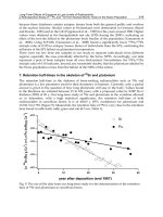
The calculated results are shown in Figs. 13 and 14. If the criterion of reflection is -20 dB,
then the bandwidth of |S
11
| in the low-frequency region is rather narrow. However, |S
21
|
is rather small and almost all of the power from port 1 is led to port 3 at high frequencies.
Port isolation between ports 2 and 3 is larger than 20 dB at frequencies between 15.3 and
16.3 GHz, as shown in Fig. 15.
7. Confirmation of mode conversion
Mode conversion of the electromagnetic waves may occur after passing through the bend
from port 3 to port 1 because dielectric arrays are absent in the straight waveguide portion.
Only the TE
20
mode needs to be considered, because the TE
30
mode is under the cutoff
condition below 19.6 GHz. The power ratio of the TE
20
to TE
10
electromagnetic wave is
obtained at port 1. The calculated results are shown in Fig. 16. Since the power of the TE
20
mode is very low at frequencies higher than 13.1 GHz, mode conversion will not occur
without dielectric rods in the straight portion.
13 14 15 16 17
-50
-40
-30
-20
-10
0
Power Ratio (TE
20
/TE
10
) [dB]
Frequency [GHz]
Fig. 16. Power ratio of TE
20
to TE
10
at port 1.
8. Simple fabrication method
As shown in the previous section, holes with diameters slightly larger than the rods will be
fabricated at the top of the waveguide and the dielectric rods will be inserted (Type B, Fig.
11).
Firstly, the thick Teflon rod needs to be replaced by a thin LaAlO
3
rod. Fig. 17 shows an
improved structure over that shown in Fig. 12. The coordinates and radii of the dielectric
rods are shown in Table 1. A thick dielectric rod will be replaced by two thin LaAlO
3
rods
having radii of 0.36 mm at separated by 7.9 mm. The S-parameters calculated by HFSS are
shown by the solid lines in Figs. 18 and 19. Secondly, S-parameters are calculated for type B
in Fig. 11 with two thin LaAlO
3
rods inserted from the top of the waveguide. The diameter
for inserting three thin rods is assumed to be 0.8 mm. The S-parameters calculated by HFSS
are shown by the dotted lines in Figs. 18 and 19. The results for the solid and dotted lines are
almost the same. Port isolation between ports 2 and 3 is shown in Fig. 20.
1mm
Port 2
Port 1
Port 3
Thin dielectric
rods
r
=0.36mm
7.9mm
22.9mm
15.8m
m
Origin
x
y
Rod 1
2
3
4
5
9
6
7
8
Fig. 17. Improved structure of the frequency multiplexer/demultiplexer. Two thin LaAlO
3
rods are used to reduce reflections.
Rod No. Coordinate
x [mm]
Coordinate
y [mm]
Radius
r [mm]
1 1.26 -0.29 0.83
2 10.3 1.2 0.86
3 17.1 7.3 0.86
4 19.7 16.1 0.83
5 19.7 25.2 0.83
6 3.2 16.1 0.83
7 3.2 25.2 0.83
8 7.5 26.2 0.36
9 15.4 26.2 0.36
Table 1. Coordinates and radii of dielectric rods illustrated in Fig. 17
ADual-FrequencyMetallicWaveguideSystem 325
The calculated results are shown in Figs. 13 and 14. If the criterion of reflection is -20 dB,
then the bandwidth of |S
11
| in the low-frequency region is rather narrow. However, |S
21
|
is rather small and almost all of the power from port 1 is led to port 3 at high frequencies.
Port isolation between ports 2 and 3 is larger than 20 dB at frequencies between 15.3 and
16.3 GHz, as shown in Fig. 15.
7. Confirmation of mode conversion
Mode conversion of the electromagnetic waves may occur after passing through the bend
from port 3 to port 1 because dielectric arrays are absent in the straight waveguide portion.
Only the TE
20
mode needs to be considered, because the TE
30
mode is under the cutoff
condition below 19.6 GHz. The power ratio of the TE
20
to TE
10
electromagnetic wave is
obtained at port 1. The calculated results are shown in Fig. 16. Since the power of the TE
20
mode is very low at frequencies higher than 13.1 GHz, mode conversion will not occur
without dielectric rods in the straight portion.
13 14 15 16 17
-50
-40
-30
-20
-10
0
Power Ratio (TE
20
/TE
10
) [dB]
Frequency [GHz]
Fig. 16. Power ratio of TE
20
to TE
10
at port 1.
8. Simple fabrication method
As shown in the previous section, holes with diameters slightly larger than the rods will be
fabricated at the top of the waveguide and the dielectric rods will be inserted (Type B, Fig.
11).
Firstly, the thick Teflon rod needs to be replaced by a thin LaAlO
3
rod. Fig. 17 shows an
improved structure over that shown in Fig. 12. The coordinates and radii of the dielectric
rods are shown in Table 1. A thick dielectric rod will be replaced by two thin LaAlO
3
rods
having radii of 0.36 mm at separated by 7.9 mm. The S-parameters calculated by HFSS are
shown by the solid lines in Figs. 18 and 19. Secondly, S-parameters are calculated for type B
in Fig. 11 with two thin LaAlO
3
rods inserted from the top of the waveguide. The diameter
for inserting three thin rods is assumed to be 0.8 mm. The S-parameters calculated by HFSS
are shown by the dotted lines in Figs. 18 and 19. The results for the solid and dotted lines are
almost the same. Port isolation between ports 2 and 3 is shown in Fig. 20.
1mm
Port 2
Port 1
Port 3
Thin dielectric
rods
r
=0.36mm
7.9mm
22.9mm
15.8m
m
Origin
x
y
Rod 1
2
3
4
5
9
6
7
8
Fig. 17. Improved structure of the frequency multiplexer/demultiplexer. Two thin LaAlO
3
rods are used to reduce reflections.
Rod No. Coordinate
x [mm]
Coordinate
y [mm]
Radius
r [mm]
1 1.26 -0.29 0.83
2 10.3 1.2 0.86
3 17.1 7.3 0.86
4 19.7 16.1 0.83
5 19.7 25.2 0.83
6 3.2 16.1 0.83
7 3.2 25.2 0.83
8 7.5 26.2 0.36
9 15.4 26.2 0.36
Table 1. Coordinates and radii of dielectric rods illustrated in Fig. 17
MicrowaveandMillimeterWaveTechnologies:ModernUWBantennasandequipment326
8 10 12 14 16
-40
-30
-20
-10
0
|S| [dB]
Frequency [GHz]
S
11
(=S
22
)
S
11
S
33
Fig. 18. Reflection coefficient |S
11
| (=|S
22
|) for low frequencies and |S
11
| and |S
33
| for high
frequencies. Solid and dotted lines denote the cases for type A and type B illustrated in Fig.9,
respectively.
8 10 12 14 16
-20
-15
-10
-5
0
|S| [dB]
Frequency [GHz]
S
21
(=S
12
)
S
31
S
21
Fig. 19. |S
21
| (=|S
12
|) for low frequencies and |S
21
| and |S
31
| for high frequencies. Solid
and dotted lines denote the cases for type A and type B illustrated in Fig.9, respectively.
13 14 15 16 17
0
10
20
30
40
Isolation [dB] (Port3 -Port 2)
Frequency [GHz]
S
31
-S
21
Fig. 20. Port isolation between two output ports. Solid and dotted lines denote the cases for
type A and type B illustrated in Fig.9, respectively.
9. Conclusion
Electromagnetic waves were propagated in a waveguide with dual in-line dielectric rods
made of LaAlO
3
and without higher modes above 2f
c
. Firstly, an economically feasible setup
for this type of waveguide system was proposed including 90° bend waveguide. Reflection
coefficients |S
11
| smaller than -18 dB were obtained at frequencies between 8.2 and 9.1 GHz
and between 15.3 and 16.8 GHz by calculation. The electromagnetic wave includes less than
-40 dB of the TE
20
component in the straight portion in the case of a radius of curvature R ≥
38.5 mm at frequencies below 17 GHz, so that dielectric rods are not required in the straight
portion.
Secondly, a sample structure for a frequency multiplexer/demultiplexer is proposed for
introducing electromagnetic waves from a coaxial cable. Reflection of electromagnetic wave
occurs without dielectric rods in the straight portion; therefore, another rod, made of LaAlO
3
or Teflon, is introduced to reduce reflection and the calculated S-parameters. The
bandwidths for reflections smaller than -20 dB are still narrow; however, optimization of the
design may enable the bandwidth to be expanded.
ADual-FrequencyMetallicWaveguideSystem 327
8 10 12 14 16
-40
-30
-20
-10
0
|S| [dB]
Frequency [GHz]
S
11
(=S
22
)
S
11
S
33
Fig. 18. Reflection coefficient |S
11
| (=|S
22
|) for low frequencies and |S
11
| and |S
33
| for high
frequencies. Solid and dotted lines denote the cases for type A and type B illustrated in Fig.9,
respectively.
8 10 12 14 16
-20
-15
-10
-5
0
|S| [dB]
Frequency [GHz]
S
21
(=S
12
)
S
31
S
21
Fig. 19. |S
21
| (=|S
12
|) for low frequencies and |S
21
| and |S
31
| for high frequencies. Solid
and dotted lines denote the cases for type A and type B illustrated in Fig.9, respectively.
13 14 15 16 17
0
10
20
30
40
Isolation [dB] (Port3 -Port 2)
Frequency [GHz]
S
31
-S
21
Fig. 20. Port isolation between two output ports. Solid and dotted lines denote the cases for
type A and type B illustrated in Fig.9, respectively.
9. Conclusion
Electromagnetic waves were propagated in a waveguide with dual in-line dielectric rods
made of LaAlO
3
and without higher modes above 2f
c
. Firstly, an economically feasible setup
for this type of waveguide system was proposed including 90° bend waveguide. Reflection
coefficients |S
11
| smaller than -18 dB were obtained at frequencies between 8.2 and 9.1 GHz
and between 15.3 and 16.8 GHz by calculation. The electromagnetic wave includes less than
-40 dB of the TE
20
component in the straight portion in the case of a radius of curvature R ≥
38.5 mm at frequencies below 17 GHz, so that dielectric rods are not required in the straight
portion.
Secondly, a sample structure for a frequency multiplexer/demultiplexer is proposed for
introducing electromagnetic waves from a coaxial cable. Reflection of electromagnetic wave
occurs without dielectric rods in the straight portion; therefore, another rod, made of LaAlO
3
or Teflon, is introduced to reduce reflection and the calculated S-parameters. The
bandwidths for reflections smaller than -20 dB are still narrow; however, optimization of the
design may enable the bandwidth to be expanded.
MicrowaveandMillimeterWaveTechnologies:ModernUWBantennasandequipment328
10. References
Ansoft Corporation (2005). Introduction to the Ansoft Macro Language, HFSS v10.
Benisty, H. (1996). Modal analysis of optical guides with two-dimensional photonic band-
gap boundaries, Journal of Applied Physics, 79, 10, (1996) pp.7483-7492, ISSN 0021-
8979.
Boroditsky, M.; Coccioli, R. & Yablonovitch, E. (1998). Analysis of photonic crystals for light
emitting diodes using the finite difference time domain technique, Proceedings of
SPIE, Vol. 3283, (1998) pp.184-190, ISSN 0277-786X.
Cohn, S., B. (1947). Properties of Ridge Wave Guide, Proceedings of the IRE, Vol.35, (Aug.
1947) pp. 783-788, ISSN 0096-8390.
Kokubo, Y.; Maki, D. & Kawai, T. (2007a). Dual-Band Metallic Waveguide with Low
Dielectric Constant Material, 37th European Microwave Conference Proceedings,
pp.890-892, ISBN 978-2-87487-000-2, Munich, Germany, Oct. 2007, EuMA, Belgium.
Kokubo, Y.; Yoshida, S. & Kawai, T. (2007b). Economic Setup for a Dual-band Metallic
Waveguide with Dual In-line Dielectric Rods, IEICE Transactions on Electronics,
Vol.E90-C, No.12, (Dec. 2007) pp.2261-2262, ISSN 0916-8524.
Kokubo, Y. & Kawai, T. (2008). A Frequency Multiplexer/Demultiplexer for Dual Frequency
Waveguide, 38th European Microwave Conference Proceedings, (Oct. 2008) pp.24-27,
ISBN 978-2-87487-005-7, Amsterdam, The Netherland, Oct. 2008, EuMA, Belgium.
Maradudin, A. A. & McGurn, A. R. (1993). Photonic band structure of a truncated, two-
dimensional, periodic dielectric medium, Journal of the Optical Society of America B,
Vol.10, No.2, (1993) pp. 307-313, ISSN 0740-3224.
Shibano, T.; Maki, D. & Kokubo, Y. (2006). Dual Band Metallic Waveguide with Dual in-line
Dielectric Rods, IEICE Transactions on Electronics, Vol.J89-C, No.10, (Oct. 2006)
pp.743-744, ISSN 1345-2827 (Japanese Edition) ; Correction and supplement, ibid,
Vol.J90-C, No.3, (Mar. 2007) p.298, ISSN 1345-2827. (Japanese Edition).
Tayeb, G. & Maystre, D. (1997). Rigorous theoretical study of finite-size two-dimensional
photonic crystals doped by microcavities, Journal of the Optical Society of America A,
Vol. 14, No.12, (Dec. 1997) pp. 3323-3332, ISSN 1084-7529.
ApplicationsofOn-ChipCoplanarWaveguidestoDesign
LocalOscillatorsforWirelessCommunicationsSystem 329
Applications of On-Chip Coplanar Waveguides to Design Local
OscillatorsforWirelessCommunicationsSystem
RameshK.Pokharel,HaruichiKanayaandKeijiYoshida
x
Applications of On-Chip Coplanar
Waveguides to Design Local
Oscillators for Wireless
Communications System
Ramesh K. Pokharel, Haruichi Kanaya
and Keiji Yoshida
Kyushu University
Japan
1. Introduction
On-chip distributed transmission line resonators in CMOS technology have become the
interest of research subjects recently (Ono et al. 2001; Umeda et al., 1994; Kanaya et al., 2006;
Wolf, 2006) because of their size which becomes more compact, as the frequency of
application increases. Among the various transmission lines, coplanar waveguide (CPW)
has more engineering applications (Toyoda, 1996; Civello, 2005) because it is easy to
fabricate by LSI technology since the signal line and ground plane exist on the same plane so
that no via holes are required for integrating active components such as transistors on Si-
substrate (Toyoda, 1996).
The applications of the CPW were reported for many on-chip LSI components. The CPW
was exploited as an inductor and used to design a conventional-type matching circuit for
LNA (Ono et al., 2001) in microwave-band frequency, and they are most popular in
monolithic microwave integrated circuit (MMIC) (Umeda et al., 1994). However, the
application of CPW lines as an inductor takes larger space than the conventional spiral
inductors (Umeda et al., 1994). Some of the present authors have also implemented the on-
chip CPW impedance-matching circuit for a 2.4 GHz RF front-end (Kanaya et al., 2006) and
for 5GHz band power amplifier (Pokharel et al., 2008) using impedance inverters. In
designing the matching circuits using impedance inverters and quarter wavelength
resonators realized by on-chip CPW (Kanaya et al, 2006; Pokharel et al., 2008) the size of the
matching circuits becomes compact thus reducing the chip area by about 30% than using
spiral inductors for 2.4GHz-band applications and 40% for 5 GHz-band applications.
However, the applications of on-chip CPW resonators in designing other components such
as a voltage-controlled oscillator (VCO) have not been reported yet. A conventional VCO
consists of a LC-resonator to produce an oscillation at the frequency band of interest, and
this LC-resonator may be replaced by a CPW resonator. Such possibilities are investigated in
this paper. In a conventional VCO, the performance such as phase noise of the VCO
depends on the quality (Q) factor of the LC resonator. Usually, a spiral inductor is used in
17
MicrowaveandMillimeterWaveTechnologies:ModernUWBantennasandequipment330
the resonator and these have quite low Q’s of around 3-5 at GHz frequency range and on the
other hand, it takes large on-chip area in the expensive silicon substrate. The inductor can be
either resonated with the device drain capacitance or by adding a shunt capacitor (on chip
or off). Using bond wires instead of on-chip spiral inductors allows the design of low phase
noise oscillators but makes the fabrication more difficult as it is difficult to precisely set the
length of the bond wire. Also for use in Phase Locked Loop (PLL) applications it is
necessary to have variable frequency or so called higher frequency tuning range (FTR).
Therefore, it is not a wise practice to use bond wires in designing a VCO due to design
difficulties in estimating the bond wires inductances.
In this paper, first, we propose a design method of a VCO using on-chip CPW resonator
thus replacing an LC-resonator. First, transmission characteristics of the on-chip meander
CPW resonator fabricated using TSMC 0.18 m CMOS technology are investigated
experimentally and an equivalent circuit is developed. Later, the application of on-chip
resonator is also demonstrated to design 10 bits digitally-controlled oscillator (DCO). The
derived equivalent circuit is used to carry out the post-layout simulation of the chip. One of
the advantages of the proposed method to design VCO and DCO using on-chip CPW
resonator than using a LC-resonator is smaller chip area.
2. Design of On-Chip CPW Resonator and Its Equivalent Circuits
In this paper, we use Advanced Design System (ADS2008A, Agilent Technologies) for
designing active elements and Momentum (Agilent Technologies) for passive elements for
schematic design. Co-simulation option was used for electromagnetic characterization of
hybrid structures consisting of active and passive elements together. We first develop the
equivalent circuit for on-chip meander CPW resonator using experimental results and latter,
the circuit is used to carry out the post-layout simulation of the chip.
The on-chip meander CPW resonator is designed, fabricated, and measured using TSMC
0.18 m CMOS technology. This process has 1-poly and 6-metal layers and the thickness of
the top metal is 3.1 m. The conductance of the metal and dielectric permittivity (
r
) of the
SiO
2
are 4.1x10
7
S/m and 4.1, respectively. The upper layer is covered by lamination whose
relative permittivity is 7.9.
Fig. 1 shows the layout and chip photos of on-chip CPW resonator designed and
characterized by EM simulator. In Fig. 1(a), the enlarged portion of the layout is illustrated
to show its structure in detail where the signal line and slot size is 5 m each, respectively.
Bottom metal (Metal-1) is used as ground plane covering all portion of CPW to reduce the
losses. Therefore, we prefer to call this CPW as conductor-backed CPW. Total length of the
resonator is 3300 m which is supposed to be shorter than a quarter-wavelength resonator at
5.2 GHz. The chip photo of the on-chip CPW resonator is shown in Fig. 1(b) and Fig. 1(c).
Please note that a small stub at the center CPW pad (dummy pad of right side) in Fig. 1(b) is
to de-embed the interconnect between metal 6 terminal of the CPW resonator and the pad.
The microwave characteristics are measured by using air coplanar probes (Cascade
Microtech, GSG150) and vector network analyzer (HP, HP8722C) in Air coplanar probe
station (Cascade Microtech Inc.). The CPW pads are 100m square and have coplanar
configurations so that characteristic impedance is 50 .
(a) Layout of CPW resonator showing enlarged section for illustration of its structure
(b) Dummy chip (c) On-chip CPW meander resonator
Fig. 1. Layouts and chip photographs of CPW resonator.
The measured data must be de-embedded in order to remove the parasitic effects of
interconnects, pads and contacts surrounding the device (Civello, 2005). Therefore, in Fig.
1(b), chip photo of a dummy pad and in Fig. 1(c), chip photo of the CPW resonator are
shown. In order to de-embed the measured raw data, at first, we measure S-parameters of
total (Fig. 1(c)) and open dummy chip (Fig. 1(b)), respectively. Next, S-parameters are
transformed into Y-parameters according to Equation (1) to get the Y-parameters (Y
TML
) of
the transmission-line resonator only.
(1)
Y-parameters are then converted to Z-parameters in order to compare the results between
simulation using the Equivalent circuits of Fig. 2. In Fig. 2, two equivalent circuits are
developed using 2-stages and 5-stages for CPW resonator in meander structure, where ideal
transmission lines are represented by the parameters such as characteristic impedance (Z0),
electrical length of each part (E), and frequency (F). Furthermore, C
1
represents the mutual
capacitance between the meander lines, R
1
is the resistive loss of the line in each segment,
and the parameters R (resistance), C (Capacitance) represent the silicon substrate of the
corresponding segment. In Fig. 2(b), where 5-stage model of equivalent circuit is shown, the
meander line is divided into shorter segments, therefore parameters of each segment of the
model such as R
1
, C
1
, E will differ from 2-stage model of Fig. 2(a). Each parameters in both
models are noted below each figure. Here, model parameters for Si-substrate (R, C) are
TML total dumm
y
[ ] [ ] [ ]Y Y Y
Ground
Ground
Signal
Ground
Ground
Signal
ApplicationsofOn-ChipCoplanarWaveguidestoDesign
LocalOscillatorsforWirelessCommunicationsSystem 331
the resonator and these have quite low Q’s of around 3-5 at GHz frequency range and on the
other hand, it takes large on-chip area in the expensive silicon substrate. The inductor can be
either resonated with the device drain capacitance or by adding a shunt capacitor (on chip
or off). Using bond wires instead of on-chip spiral inductors allows the design of low phase
noise oscillators but makes the fabrication more difficult as it is difficult to precisely set the
length of the bond wire. Also for use in Phase Locked Loop (PLL) applications it is
necessary to have variable frequency or so called higher frequency tuning range (FTR).
Therefore, it is not a wise practice to use bond wires in designing a VCO due to design
difficulties in estimating the bond wires inductances.
In this paper, first, we propose a design method of a VCO using on-chip CPW resonator
thus replacing an LC-resonator. First, transmission characteristics of the on-chip meander
CPW resonator fabricated using TSMC 0.18 m CMOS technology are investigated
experimentally and an equivalent circuit is developed. Later, the application of on-chip
resonator is also demonstrated to design 10 bits digitally-controlled oscillator (DCO). The
derived equivalent circuit is used to carry out the post-layout simulation of the chip. One of
the advantages of the proposed method to design VCO and DCO using on-chip CPW
resonator than using a LC-resonator is smaller chip area.
2. Design of On-Chip CPW Resonator and Its Equivalent Circuits
In this paper, we use Advanced Design System (ADS2008A, Agilent Technologies) for
designing active elements and Momentum (Agilent Technologies) for passive elements for
schematic design. Co-simulation option was used for electromagnetic characterization of
hybrid structures consisting of active and passive elements together. We first develop the
equivalent circuit for on-chip meander CPW resonator using experimental results and latter,
the circuit is used to carry out the post-layout simulation of the chip.
The on-chip meander CPW resonator is designed, fabricated, and measured using TSMC
0.18 m CMOS technology. This process has 1-poly and 6-metal layers and the thickness of
the top metal is 3.1 m. The conductance of the metal and dielectric permittivity (
r
) of the
SiO
2
are 4.1x10
7
S/m and 4.1, respectively. The upper layer is covered by lamination whose
relative permittivity is 7.9.
Fig. 1 shows the layout and chip photos of on-chip CPW resonator designed and
characterized by EM simulator. In Fig. 1(a), the enlarged portion of the layout is illustrated
to show its structure in detail where the signal line and slot size is 5 m each, respectively.
Bottom metal (Metal-1) is used as ground plane covering all portion of CPW to reduce the
losses. Therefore, we prefer to call this CPW as conductor-backed CPW. Total length of the
resonator is 3300 m which is supposed to be shorter than a quarter-wavelength resonator at
5.2 GHz. The chip photo of the on-chip CPW resonator is shown in Fig. 1(b) and Fig. 1(c).
Please note that a small stub at the center CPW pad (dummy pad of right side) in Fig. 1(b) is
to de-embed the interconnect between metal 6 terminal of the CPW resonator and the pad.
The microwave characteristics are measured by using air coplanar probes (Cascade
Microtech, GSG150) and vector network analyzer (HP, HP8722C) in Air coplanar probe
station (Cascade Microtech Inc.). The CPW pads are 100m square and have coplanar
configurations so that characteristic impedance is 50 .
(a) Layout of CPW resonator showing enlarged section for illustration of its structure
(b) Dummy chip (c) On-chip CPW meander resonator
Fig. 1. Layouts and chip photographs of CPW resonator.
The measured data must be de-embedded in order to remove the parasitic effects of
interconnects, pads and contacts surrounding the device (Civello, 2005). Therefore, in Fig.
1(b), chip photo of a dummy pad and in Fig. 1(c), chip photo of the CPW resonator are
shown. In order to de-embed the measured raw data, at first, we measure S-parameters of
total (Fig. 1(c)) and open dummy chip (Fig. 1(b)), respectively. Next, S-parameters are
transformed into Y-parameters according to Equation (1) to get the Y-parameters (Y
TML
) of
the transmission-line resonator only.
(1)
Y-parameters are then converted to Z-parameters in order to compare the results between
simulation using the Equivalent circuits of Fig. 2. In Fig. 2, two equivalent circuits are
developed using 2-stages and 5-stages for CPW resonator in meander structure, where ideal
transmission lines are represented by the parameters such as characteristic impedance (Z0),
electrical length of each part (E), and frequency (F). Furthermore, C
1
represents the mutual
capacitance between the meander lines, R
1
is the resistive loss of the line in each segment,
and the parameters R (resistance), C (Capacitance) represent the silicon substrate of the
corresponding segment. In Fig. 2(b), where 5-stage model of equivalent circuit is shown, the
meander line is divided into shorter segments, therefore parameters of each segment of the
model such as R
1
, C
1
, E will differ from 2-stage model of Fig. 2(a). Each parameters in both
models are noted below each figure. Here, model parameters for Si-substrate (R, C) are
TML total dumm
y
[ ] [ ] [ ]Y Y Y
Ground
Ground
Signal
Ground
Ground
Signal
MicrowaveandMillimeterWaveTechnologies:ModernUWBantennasandequipment332
estimated by the dielectric characteristics, and the rest of the parameters of the meander line
are estimated by fitting to the measured results, because our main goal is to develop a
simple model which can be incorporated in ADE simulation to carry out the post-layout
simulation of the chip that consists of on-chip CPW resonators.
(a) 2-stage equivalent circuit
(b) 5-stage equivalent circuit
Fig. 2. Two types of equivalent circuits using various stages for on-chip CPW meander
resonator
50-Ohm Port
2R
C/2
R
C
Z
0
, E, F
C
1
R
1
Z
0
, E, F
R
1
Parameters
Z
0
= 32 ; E= 22.5 degrees; F=1 GHz
C= 30fF; R= 8.3 k
R
1
= 14
C
1
=0.46fF;
50-Ohm Port
C
1
C/2
2R
Parameters
Z0= 32 ; E= 9 degrees; F=1 GHz
C= 11.5fF; R= 3.3 k
R
1
= 5.7
C
1
=1.1fF;
C
C
1
C
1
C
1
C
1
C
1
50-Ohm Port
50-Ohm Port
R
1
R
1
R
1
R
1
R
1
Z
0
, E, F Z
0
, E, F
Z
0
, E, F
Z
0
, E, F Z
0
, E, F
C/2
C/2
2R
2R
R
R
RR
CCC
(a) Real part of Z
11
(b) Imaginary part of Z
11
Fig. 3. Comparison of simulated Z
11
-parameters using two-types of equivalent circuit
models with Momentum-simulation and measured results
(a) Real part of Z
21
50
Real [ Z11 ] [ Ohms ]
Experiment
Momentum
Frequency [ GHz ]
5-stage eq. ckt.
2-stage eq. ckt.
2
0
10
20
30
40
12
10
86
4
-800
-600
-400
-200
0
200
2 4 6 8 10 12
Im. [ Z11 ] [ Ohms ]
Frequency [ GHz ]
Momentum
2-stage eq. ckt.
5-stage eq. ckt.
Experiment
-30
-20
-10
0
10
20
2 4 6 8 10 12
Experiment
Momentum
Frequency [ GHz ]
2-stage eq. ckt.
Real [ Z21 ] [ Ohms ]
5-stage eq. ckt.
ApplicationsofOn-ChipCoplanarWaveguidestoDesign
LocalOscillatorsforWirelessCommunicationsSystem 333
estimated by the dielectric characteristics, and the rest of the parameters of the meander line
are estimated by fitting to the measured results, because our main goal is to develop a
simple model which can be incorporated in ADE simulation to carry out the post-layout
simulation of the chip that consists of on-chip CPW resonators.
(a) 2-stage equivalent circuit
(b) 5-stage equivalent circuit
Fig. 2. Two types of equivalent circuits using various stages for on-chip CPW meander
resonator
50-Ohm Port
2R
C/2
R
C
Z
0
, E, F
C
1
R
1
Z
0
, E, F
R
1
Parameters
Z
0
= 32 ; E= 22.5 degrees; F=1 GHz
C= 30fF; R= 8.3 k
R
1
= 14
C
1
=0.46fF;
50-Ohm Port
C
1
C/2
2R
Parameters
Z0= 32 ; E= 9 degrees; F=1 GHz
C= 11.5fF; R= 3.3 k
R
1
= 5.7
C
1
=1.1fF;
C
C
1
C
1
C
1
C
1
C
1
50-Ohm Port
50-Ohm Port
R
1
R
1
R
1
R
1
R
1
Z
0
, E, F Z
0
, E, F
Z
0
, E, F
Z
0
, E, F Z
0
, E, F
C/2
C/2
2R
2R
R
R
RR
CCC
(a) Real part of Z
11
(b) Imaginary part of Z
11
Fig. 3. Comparison of simulated Z
11
-parameters using two-types of equivalent circuit
models with Momentum-simulation and measured results
(a) Real part of Z
21
50
Real [ Z11 ] [ Ohms ]
Experiment
Momentum
Frequency [ GHz ]
5-stage eq. ckt.
2-stage eq. ckt.
2
0
10
20
30
40
12
10
86
4
-800
-600
-400
-200
0
200
2 4 6 8 10 12
Im. [ Z11 ] [ Ohms ]
Frequency [ GHz ]
Momentum
2-stage eq. ckt.
5-stage eq. ckt.
Experiment
-30
-20
-10
0
10
20
2 4 6 8 10 12
Experiment
Momentum
Frequency [ GHz ]
2-stage eq. ckt.
Real [ Z21 ] [ Ohms ]
5-stage eq. ckt.
MicrowaveandMillimeterWaveTechnologies:ModernUWBantennasandequipment334
(b) Imaginary part of Z
21
Fig. 4. Comparison of simulated Z
21
-parameters using two-types of equivalent circuit
models with Momentum-simulation and measured results
Fig. 5. Schematic of conventional VCO employing LC-resonator
buffer
buffer
Out (0-degree)
Out (180-degree)
V
dd
LC- resonator
V
count
V
bias
Cross-coupled
transconductance
-1000
-800
-600
-400
-200
0
2 4 6 8 10 12
Momentum
Experiment
5-Sta
g
e Eq. Ckt.
2-Stage Eq. Ckt.
Frequency [ GHz ]
Im. [ Z21 ] [ Ohms ]
Fig. 6. Schematic of Proposed VCO employing on-chip CPW resonator
(a) Simulation results of VCO using LC-resonator having differential output waveforms
(b) Simulation results of VCO using on-chip CPW-resonator having differential output
waveforms
Fig. 7. Output voltage waveforms of designed VCOs
50 100 150 200 2500 300
0.2
0.4
0.6
0
0.8
Time [ps ]
Voltage [ V ]
50 100 150 200 2500 300
0.2
0.4
0.6
0
0.8
Time [ps ]
Voltage [ V ]
0.0
0.2
0.4
0.6
0.8
1.0
-0.2
1.2
50 100 150 200 250 3000
Time [ps]
350 400
Voltage [ V ]
0.0
0.2
0.4
0.6
0.8
1.0
-0.2
1.2
50 100 150 200 250 3000
Time [ps]
350 400
Voltage [ V ]
buffer
buffer
Out (0-degree)
Out (180-de
g
ree)
V
dd
CPW resonator
V
count
V
bias
ApplicationsofOn-ChipCoplanarWaveguidestoDesign
LocalOscillatorsforWirelessCommunicationsSystem 335
(b) Imaginary part of Z
21
Fig. 4. Comparison of simulated Z
21
-parameters using two-types of equivalent circuit
models with Momentum-simulation and measured results
Fig. 5. Schematic of conventional VCO employing LC-resonator
buffer
buffer
Out (0-degree)
Out (180-degree)
V
dd
LC- resonator
V
count
V
bias
Cross-coupled
transconductance
-1000
-800
-600
-400
-200
0
2 4 6 8 10 12
Momentum
Experiment
5-Sta
g
e Eq. Ckt.
2-Stage Eq. Ckt.
Frequency [ GHz ]
Im. [ Z21 ] [ Ohms ]
Fig. 6. Schematic of Proposed VCO employing on-chip CPW resonator
(a) Simulation results of VCO using LC-resonator having differential output waveforms
(b) Simulation results of VCO using on-chip CPW-resonator having differential output
waveforms
Fig. 7. Output voltage waveforms of designed VCOs
50 100 150 200 2500 300
0.2
0.4
0.6
0
0.8
Time [ps ]
Voltage [ V ]
50 100 150 200 2500 300
0.2
0.4
0.6
0
0.8
Time [ps ]
Voltage [ V ]
0.0
0.2
0.4
0.6
0.8
1.0
-0.2
1.2
50 100 150 200 250 3000
Time [ps]
350 400
Voltage [ V ]
0.0
0.2
0.4
0.6
0.8
1.0
-0.2
1.2
50 100 150 200 250 3000
Time [ps]
350 400
Voltage [ V ]
buffer
buffer
Out (0-degree)
Out (180-de
g
ree)
V
dd
CPW resonator
V
count
V
bias
MicrowaveandMillimeterWaveTechnologies:ModernUWBantennasandequipment336
Finally, the Z-parameters which are transformed from S-parameters are compared with
measured results and simulation by Momentum in Fig. 3 and Fig. 4, respectively. Here we
choose Z-parameters because of the simplicity to illustrate the comparison in closer range in
linear scale. In Fig. 3, real and imaginary parts of Z
11
-parameters are compared where circuit
simulation results using the proposed equivalent circuits will reproduce more closely with
measured results than the simulation by Momentum. This tendency is also similar in Fig. 4
where real and imaginary parts of Z
21
-parameters are compared. Up to 7 GHz, both
equivalent circuits produce good agreement with the experiment results, therefore in this
paper, 2-stage equivalent circuit of Fig. 2(a) is used onwards in ADE simulation to carry out
the post-layout simulation of the whole chip of VCO employing on-chip CPW resonator.
3. Design of VCO Using On-Chip CPW Resonator
A conventional VCO (Dai & Harjani, 2003; Hajimiri & Lee, 2004) mainly consists of three
parts such as (i) LC-resonator (ii) Varactor (iii) Cross-coupled transconductance circuit as
shown in Fig. 5 where the LC tank circuit determines the frequency of oscillation and form
the drain loads. Frequency dependant signals at the drains are then ‘cross-coupled’ to the
other devices’ gate, which creates a negative impedance of value –1/gm at the drain
terminals. As VCO is usually used in a phase-locked loop (PLL) in a wireless transceiver, it
is necessary to have variable frequency, which is measured in terms of frequency tuning
range (FTR) corresponding to center frequency. To make the fixed frequency oscillator into a
variable frequency oscillator, it is necessary to tune the capacitive load and for this purpose,
a voltage-tuned capacitor known as varactor is added into the resonator.
Fig. 5 and Fig. 6 show the schematics of the designed VCOs. In Fig. 5, schematic of LC-VCO
is shown and that of using the proposed CPW resonator is shown in Fig. 6. In Fig. 5, the
parasitic capacitances of the 1/gm devices will increase the minimum capacitance of the
varacter reducing the tuning range of the VCO whereas in Fig. 6, the equivalent capacitance
of the varacter and CPW resonator will decrease which results in the higher FTR of the
proposed VCO using on-chip CPW resonator which is to be illustrated in Fig. 11.
Fig. 7 shows the post-layout simulation of waveforms of the maximum voltage swing of the
designed VCO where the maximum peak voltage of LC-VCO is greater than that of the VCO
using on-chip CPW resonator and this is clearly reflected in the performance of the phase
noise of the VCO in Table 1 to be discussed later.
4. Fabricated Chips and Measurement Results
We designed, fabricated and measured two VCOs as shown in the schematics of Fig. 5 and
Fig. 6, respectively for comparison purpose. However, from onward, we will present the
graphs of measured results of the proposed VCO using on-chip CPW resonator only and
will summarize the final results of both VCOs in Table 1.
Fig. 8 shows the chip photo of the proposed VCO that employs on-chip CPW resonator. The
output of both VCOs is designed with buffer circuits so that it provides good matching with
the measurement equipments such a spectrum analyzer. Phase noise of the VCO is
measured using a Signal Source Analyzer (E5052B SSA, Agilent Technologies) and keeping
the chip inside a shield box. While measuring the phase noise of the VCO, the chip was
placed inside a small shield room to protect the phase noise from the effect of the low-
frequencies inference, therefore we designed both VCOs with SMA connecter rather than
CPW probes because, if we design the VCO with the pads for the CPW coplanar probes, we
can not measure inside a shield box.
Fig. 8. Chip photograph of designed VCO using on-chip CPW resonator in TSMC 0.18m
CMOS
Fig. 9. Spectrum of output power of the VCO employing on-chip CPW resonator measured
by SSA
Fig. 10. Phase noise of the proposed VCO using on-chip CPW resonator with noise of DC
source only measured by SSA
CPW resonatorCPW resonator
Noise spectrum of DC source only
Modulated by DC
source noise
-109 dbc/Hz
(@1MHz offset)
Noise spectrum of DC source only
Modulated by DC
source noise
-109 dbc/Hz
(@1MHz offset)
ApplicationsofOn-ChipCoplanarWaveguidestoDesign
LocalOscillatorsforWirelessCommunicationsSystem 337
Finally, the Z-parameters which are transformed from S-parameters are compared with
measured results and simulation by Momentum in Fig. 3 and Fig. 4, respectively. Here we
choose Z-parameters because of the simplicity to illustrate the comparison in closer range in
linear scale. In Fig. 3, real and imaginary parts of Z
11
-parameters are compared where circuit
simulation results using the proposed equivalent circuits will reproduce more closely with
measured results than the simulation by Momentum. This tendency is also similar in Fig. 4
where real and imaginary parts of Z
21
-parameters are compared. Up to 7 GHz, both
equivalent circuits produce good agreement with the experiment results, therefore in this
paper, 2-stage equivalent circuit of Fig. 2(a) is used onwards in ADE simulation to carry out
the post-layout simulation of the whole chip of VCO employing on-chip CPW resonator.
3. Design of VCO Using On-Chip CPW Resonator
A conventional VCO (Dai & Harjani, 2003; Hajimiri & Lee, 2004) mainly consists of three
parts such as (i) LC-resonator (ii) Varactor (iii) Cross-coupled transconductance circuit as
shown in Fig. 5 where the LC tank circuit determines the frequency of oscillation and form
the drain loads. Frequency dependant signals at the drains are then ‘cross-coupled’ to the
other devices’ gate, which creates a negative impedance of value –1/gm at the drain
terminals. As VCO is usually used in a phase-locked loop (PLL) in a wireless transceiver, it
is necessary to have variable frequency, which is measured in terms of frequency tuning
range (FTR) corresponding to center frequency. To make the fixed frequency oscillator into a
variable frequency oscillator, it is necessary to tune the capacitive load and for this purpose,
a voltage-tuned capacitor known as varactor is added into the resonator.
Fig. 5 and Fig. 6 show the schematics of the designed VCOs. In Fig. 5, schematic of LC-VCO
is shown and that of using the proposed CPW resonator is shown in Fig. 6. In Fig. 5, the
parasitic capacitances of the 1/gm devices will increase the minimum capacitance of the
varacter reducing the tuning range of the VCO whereas in Fig. 6, the equivalent capacitance
of the varacter and CPW resonator will decrease which results in the higher FTR of the
proposed VCO using on-chip CPW resonator which is to be illustrated in Fig. 11.
Fig. 7 shows the post-layout simulation of waveforms of the maximum voltage swing of the
designed VCO where the maximum peak voltage of LC-VCO is greater than that of the VCO
using on-chip CPW resonator and this is clearly reflected in the performance of the phase
noise of the VCO in Table 1 to be discussed later.
4. Fabricated Chips and Measurement Results
We designed, fabricated and measured two VCOs as shown in the schematics of Fig. 5 and
Fig. 6, respectively for comparison purpose. However, from onward, we will present the
graphs of measured results of the proposed VCO using on-chip CPW resonator only and
will summarize the final results of both VCOs in Table 1.
Fig. 8 shows the chip photo of the proposed VCO that employs on-chip CPW resonator. The
output of both VCOs is designed with buffer circuits so that it provides good matching with
the measurement equipments such a spectrum analyzer. Phase noise of the VCO is
measured using a Signal Source Analyzer (E5052B SSA, Agilent Technologies) and keeping
the chip inside a shield box. While measuring the phase noise of the VCO, the chip was
placed inside a small shield room to protect the phase noise from the effect of the low-
frequencies inference, therefore we designed both VCOs with SMA connecter rather than
CPW probes because, if we design the VCO with the pads for the CPW coplanar probes, we
can not measure inside a shield box.
Fig. 8. Chip photograph of designed VCO using on-chip CPW resonator in TSMC 0.18m
CMOS
Fig. 9. Spectrum of output power of the VCO employing on-chip CPW resonator measured
by SSA
Fig. 10. Phase noise of the proposed VCO using on-chip CPW resonator with noise of DC
source only measured by SSA
CPW resonatorCPW resonator
Noise spectrum of DC source only
Modulated by DC
source noise
-109 dbc/Hz
(@1MHz offset)
Noise spectrum of DC source only
Modulated by DC
source noise
-109 dbc/Hz
(@1MHz offset)
MicrowaveandMillimeterWaveTechnologies:ModernUWBantennasandequipment338
Fig. 11. Measured frequency-tuning rage (FTR) showing comparison between FTR of the
proposed VCO with that of LC-VCO
LC resonator CPW resonator
Center
Frequency [GHz]
5.2 5.9
FTR [%] 5.4 10.9
Phase noise
[dBc/Hz@1MHz]
-114 -109
Area [
2
m ]
1.4x10
-7
1.1x10
-7
Table 1. Comparison of measured parameters between two vcos using lc resonator and on-
chip cpw resonator, respectively. [ftr=frequency-tuning range]
The output power spectrum is measured by SSA which is shown in Fig. 9. Fig. 10 shows the
measured phase noise of the proposed VCO. The phase noise measurement demands a dc
sources free from any low-frequencies noise. Among them, the relatively pure two DC
sources can be obtained from SSA but our VCO layout needs three DC sources for biasing.
Therefore, we use two DC sources from SSA and a commercial DC source for remaining one.
Due to this impure DC source, the spectrum of phase noise below 900KHz-offset frequency
in Fig. 10 is affected by noise of the DC source. The long wires that connects the DC source
and the chip that placed inside a shield box when completes a ground path with SSA, acts as
a inductance and in turn becomes a loop antenna, which is the main reason of the
modulated phase noise below 900MHz-offset frequency in Fig. 10. To clarify this issue, we
also plotted the noise spectrum of DC source only in Fig. 10 with phase noise of the VCO
and it validates the explanation above. Therefore, it is inferred that a pure DC source is
inherent to measure the phase noise of a VCO and the wires that connect the DC source and
the chip should be as short as possible.
The comparison of measured FTR of the proposed VCO employing on-chip CPW resonator
with that of LC-VCO is shown in Fig. 11 where FTR of the proposed VCO has larger FTR
than that of LC-VCO. To make the fixed frequency oscillator into a variable frequency
4.8
5.0
5.2
5.4
5.6
5.8
6.0
6.2
6.4
0 0.4 0.8 1.2 1.6
Frequency [ GHz ]
Control Voltage [ V ]
CPW-VCO
LC-VCO
4.8
5.0
5.2
5.4
5.6
5.8
6.0
6.2
6.4
0 0.4 0.8 1.2 1.6
Frequency [ GHz ]
Control Voltage [ V ]
CPW-VCO
LC-VCO
oscillator, varacter is connected as a capacitive load to a resonator. But the parasitic
capacitances of the 1/gm devices will increase the minimum capacitance of the varacter
reducing the tuning range of the conventional LC-VCO whereas in the proposed VCO, the
equivalent capacitance of the varacter and CPW resonator will decrease which results in the
higher FTR of the proposed VCO in Fig. 11.
Table 1 show the comparison of the parameters of the proposed VCO using on-chip CPW
resonator with VCO employing LC-resonator. From the table, it is noted that the VCO using
CPW resonator has advantages in terms of chip size and frequency-turning range (FTR). On
the other hand, it has slightly poor performance in terms of phase noise but this design
technique can be implemented for higher frequency applications whereas in designing a LC-
VCO, the self-resonance of inductor prevents its applications beyond that frequency.
5. Application of On-Chip CPW Resonator to Design a Digitally Controlled
Oscillator
5.1 Introduction of Digitally Controlled Oscillator (DCO)
Scaling down of CMOS technology and reduction in supply voltage complicates the
implementation of RF integrated circuits in deep submicron CMOS process and demands
the use of digital-assisted approaches in their circuit implementation (Matsuzawa, 2008). An
oscillator, being a critical component of all digital phase locked loop (ADPLL) for future
generation wireless transceiver, is necessary to be implemented using digital signals to
control its frequency tuning characteristics.
Recently, various types of DCO architectures were proposed and implemented in deep
submicron CMOS technology (Staszewski et al., 2005, Fahs et al., 2009). The DCO
implemented in ring structure (Fahs et al., 2009) gives poor phase noise performance with
high power consumption, and they are, therefore, hardly suitable for multi-GHz wireless
applications. In a DCO implemented using a LC-resonator (Staszewski et al., 2005), on-chip
inductor (L) is inherent which increases the chip size and in turn, results in high price. In
this Section, we will propose a 10bit DCO using on-chip CPW resonator and MIM capacitors
instead of the LC-resonator.
5.2 Design, Fabrication, and Experimental Results of 10 bit DCO
The proposed schematic of the designed 10 bit DCO is shown in Fig. 12 where the core of
the DCO is similar to the VCO explained in chapter 3 which employed the on-chip CPW
resonator instead of LC resonator. Furthermore, varacters are replaced by a capacitor bank
made of MIM capacitors which are controlled by 10 bit digital signals so that wide tuning
range is realized. Figure 13 shows the chip photograph of the proposed DCO to test the
proposed concept of designing a DCO using on-chip CPW resonator. The control pins were
wire bonded to a package and the package was placed on a PCB and externally controlled
similarly as in the VCO. The output of DCO is designed with buffer circuits to provide a
good matching to the measurement equipments. The measured DC power consumed by the
DUT was about 75.8 mW at 1.8 V supply, and simulation shows that about 61% of total
power was consumed by the buffer circuits only. The exact power consumption of the
proposed DCO can be predicted when two separate DC supply source were designed for
DCO core and buffer circuits, respectively. Figure 14 shows the one of the signal spectrums
measured which verifies the DCO is operating at 5.2 GHz producing the power of -16 dBm.
ApplicationsofOn-ChipCoplanarWaveguidestoDesign
LocalOscillatorsforWirelessCommunicationsSystem 339
Fig. 11. Measured frequency-tuning rage (FTR) showing comparison between FTR of the
proposed VCO with that of LC-VCO
LC resonator CPW resonator
Center
Frequency [GHz]
5.2 5.9
FTR [%] 5.4 10.9
Phase noise
[dBc/Hz@1MHz]
-114 -109
Area [
2
m ]
1.4x10
-7
1.1x10
-7
Table 1. Comparison of measured parameters between two vcos using lc resonator and on-
chip cpw resonator, respectively. [ftr=frequency-tuning range]
The output power spectrum is measured by SSA which is shown in Fig. 9. Fig. 10 shows the
measured phase noise of the proposed VCO. The phase noise measurement demands a dc
sources free from any low-frequencies noise. Among them, the relatively pure two DC
sources can be obtained from SSA but our VCO layout needs three DC sources for biasing.
Therefore, we use two DC sources from SSA and a commercial DC source for remaining one.
Due to this impure DC source, the spectrum of phase noise below 900KHz-offset frequency
in Fig. 10 is affected by noise of the DC source. The long wires that connects the DC source
and the chip that placed inside a shield box when completes a ground path with SSA, acts as
a inductance and in turn becomes a loop antenna, which is the main reason of the
modulated phase noise below 900MHz-offset frequency in Fig. 10. To clarify this issue, we
also plotted the noise spectrum of DC source only in Fig. 10 with phase noise of the VCO
and it validates the explanation above. Therefore, it is inferred that a pure DC source is
inherent to measure the phase noise of a VCO and the wires that connect the DC source and
the chip should be as short as possible.
The comparison of measured FTR of the proposed VCO employing on-chip CPW resonator
with that of LC-VCO is shown in Fig. 11 where FTR of the proposed VCO has larger FTR
than that of LC-VCO. To make the fixed frequency oscillator into a variable frequency
4.8
5.0
5.2
5.4
5.6
5.8
6.0
6.2
6.4
0 0.4 0.8 1.2 1.6
Frequency [ GHz ]
Control Voltage [ V ]
CPW-VCO
LC-VCO
4.8
5.0
5.2
5.4
5.6
5.8
6.0
6.2
6.4
0 0.4 0.8 1.2 1.6
Frequency [ GHz ]
Control Voltage [ V ]
CPW-VCO
LC-VCO
oscillator, varacter is connected as a capacitive load to a resonator. But the parasitic
capacitances of the 1/gm devices will increase the minimum capacitance of the varacter
reducing the tuning range of the conventional LC-VCO whereas in the proposed VCO, the
equivalent capacitance of the varacter and CPW resonator will decrease which results in the
higher FTR of the proposed VCO in Fig. 11.
Table 1 show the comparison of the parameters of the proposed VCO using on-chip CPW
resonator with VCO employing LC-resonator. From the table, it is noted that the VCO using
CPW resonator has advantages in terms of chip size and frequency-turning range (FTR). On
the other hand, it has slightly poor performance in terms of phase noise but this design
technique can be implemented for higher frequency applications whereas in designing a LC-
VCO, the self-resonance of inductor prevents its applications beyond that frequency.
5. Application of On-Chip CPW Resonator to Design a Digitally Controlled
Oscillator
5.1 Introduction of Digitally Controlled Oscillator (DCO)
Scaling down of CMOS technology and reduction in supply voltage complicates the
implementation of RF integrated circuits in deep submicron CMOS process and demands
the use of digital-assisted approaches in their circuit implementation (Matsuzawa, 2008). An
oscillator, being a critical component of all digital phase locked loop (ADPLL) for future
generation wireless transceiver, is necessary to be implemented using digital signals to
control its frequency tuning characteristics.
Recently, various types of DCO architectures were proposed and implemented in deep
submicron CMOS technology (Staszewski et al., 2005, Fahs et al., 2009). The DCO
implemented in ring structure (Fahs et al., 2009) gives poor phase noise performance with
high power consumption, and they are, therefore, hardly suitable for multi-GHz wireless
applications. In a DCO implemented using a LC-resonator (Staszewski et al., 2005), on-chip
inductor (L) is inherent which increases the chip size and in turn, results in high price. In
this Section, we will propose a 10bit DCO using on-chip CPW resonator and MIM capacitors
instead of the LC-resonator.
5.2 Design, Fabrication, and Experimental Results of 10 bit DCO
The proposed schematic of the designed 10 bit DCO is shown in Fig. 12 where the core of
the DCO is similar to the VCO explained in chapter 3 which employed the on-chip CPW
resonator instead of LC resonator. Furthermore, varacters are replaced by a capacitor bank
made of MIM capacitors which are controlled by 10 bit digital signals so that wide tuning
range is realized. Figure 13 shows the chip photograph of the proposed DCO to test the
proposed concept of designing a DCO using on-chip CPW resonator. The control pins were
wire bonded to a package and the package was placed on a PCB and externally controlled
similarly as in the VCO. The output of DCO is designed with buffer circuits to provide a
good matching to the measurement equipments. The measured DC power consumed by the
DUT was about 75.8 mW at 1.8 V supply, and simulation shows that about 61% of total
power was consumed by the buffer circuits only. The exact power consumption of the
proposed DCO can be predicted when two separate DC supply source were designed for
DCO core and buffer circuits, respectively. Figure 14 shows the one of the signal spectrums
measured which verifies the DCO is operating at 5.2 GHz producing the power of -16 dBm.
MicrowaveandMillimeterWaveTechnologies:ModernUWBantennasandequipment340
Phase noise of the DCO was measured similarly as VCO previously. The chip was wire
bonded to PCB as shown in Figure 13 and then to SMA connectors to facilitate to measure
the phase noise inside the shield box. The digital controls bits are inputted through the
digital pads. Figure 15 shows the phase noise of the DCO where the phase noise was to be –
114 dBc/Hz (@1 MHz offset frequency).
Fig. 12. Schematic diagram of 10 bit DCO using on-chip CPW resonator
We observed some modulated waves from the offset of 100 kHz to 800 kHz, and this is
mainly due to the noise introduced along with the digital signals and through the
interconnecting cables to the control pins.
Fig. 13. Schematic diagram of 10 bit DCO using on-chip CPW resonator
Capacitor bank
buffer
buffer
Out (0-degree)
Out (180-degree)
V
dd
B
1
B
2
B
3
B
4
B
5
B
6
B
7
B
8
B
9
B
10
10 bit control signals
CPW resonator
CPW resonator
Digital control bits
Ground pads
Ground pads
0-degree output
180-degree output
CPW resonator
Digital control bits
Ground pads
Ground pads
0-degree output
180-degree output
Digital control bits
Ground pads
Ground pads
0-degree output
180-degree output
Fig. 14. Measured signal spectrum of 10 bit DCO using on-chip CPW resonator
Fig. 15. Measured phase noise of 10 bit DCO using on-chip CPW resonator
Central freq.
[ GHz ]
Tuning step
[ kHz ]
Power dissipation
[ mW ]
Phase noise
[dBc/Hz ]
Chip
size
[ mm
2
]
Proposed
TML DCO
5.0 400 75.8 -114 0.18
LC-DCO 5.0 400 75.6 -115 0.23
Table 2. Comparison of performance of the proposed TML DCO and that of a conventional
LC-DCO
-114 dBc/Hz (@1MHz offset)-114 dBc/Hz (@1MHz offset)
ApplicationsofOn-ChipCoplanarWaveguidestoDesign
LocalOscillatorsforWirelessCommunicationsSystem 341
Phase noise of the DCO was measured similarly as VCO previously. The chip was wire
bonded to PCB as shown in Figure 13 and then to SMA connectors to facilitate to measure
the phase noise inside the shield box. The digital controls bits are inputted through the
digital pads. Figure 15 shows the phase noise of the DCO where the phase noise was to be –
114 dBc/Hz (@1 MHz offset frequency).
Fig. 12. Schematic diagram of 10 bit DCO using on-chip CPW resonator
We observed some modulated waves from the offset of 100 kHz to 800 kHz, and this is
mainly due to the noise introduced along with the digital signals and through the
interconnecting cables to the control pins.
Fig. 13. Schematic diagram of 10 bit DCO using on-chip CPW resonator
Capacitor bank
buffer
buffer
Out (0-degree)
Out (180-degree)
V
dd
B
1
B
2
B
3
B
4
B
5
B
6
B
7
B
8
B
9
B
10
10 bit control signals
CPW resonator
CPW resonator
Digital control bits
Ground pads
Ground pads
0-degree output
180-degree output
CPW resonator
Digital control bits
Ground pads
Ground pads
0-degree output
180-degree output
Digital control bits
Ground pads
Ground pads
0-degree output
180-degree output
Fig. 14. Measured signal spectrum of 10 bit DCO using on-chip CPW resonator
Fig. 15. Measured phase noise of 10 bit DCO using on-chip CPW resonator
Central freq.
[ GHz ]
Tuning step
[ kHz ]
Power dissipation
[ mW ]
Phase noise
[dBc/Hz ]
Chip
size
[ mm
2
]
Proposed
TML DCO
5.0 400 75.8 -114 0.18
LC-DCO 5.0 400 75.6 -115 0.23
Table 2. Comparison of performance of the proposed TML DCO and that of a conventional
LC-DCO
-114 dBc/Hz (@1MHz offset)-114 dBc/Hz (@1MHz offset)
MicrowaveandMillimeterWaveTechnologies:ModernUWBantennasandequipment342
Table 1 shows the comparison of the performances of the proposed 10 bit DCO and another
one is conventional 10 bit DCO that employed LC resonator which was also designed and
tested by the authors to compare the performance with the proposed DCO. In the table, it
shows that the proposed DCO has about 30% less chip area than the conventional DCO
using LC resonator under similar other parameters.
6. Conclusion
The applications of on-chip CPW resonator was demonstrated to design a VCO and DCO at
5 GHz band. First, we examined the characteristics of the on-chip resonator in meander
structure theoretically and experimentally in 0.18 m CMOS technology. Then, a VCO
employing on-chip CPW resonator instead of LC-tank resonator is proposed, designed and
fabricated using the same technology and latter a 10 bit DCO. The advantages of employing
CPW resonator is the wide frequency-tuning range, and it also saves about 30% of chip size
whereas the measured other performance of the proposed oscillators are comparable to that
of an oscillator using LC resonator. The design technique is applicable for higher frequencies.
Furthermore, the CPW resonator in meander structure can be designed to exploit the vacant
space of the layout so the chip size can be further reduced.
An equivalent circuit is developed to reproduce the experimental results of the on-chip
CPW resonator whose model parameters are useful to extract RCX (Resistance-Capacitance
extraction) of the chip.
7. Acknowledgement
This work was partly supported by a grant of Knowledge Cluster Initiative implemented by
Ministry of Education, Culture, Sports, Science and Technology (MEXT), JSPS.KAKENHI
(Wakate-B and Kiban-B), and JST-Seeds Excavation (B). This work was also partly supported
by VLSI Design and Education Center (VDEC), the University of Tokyo in collaboration
with CADENCE Corporation and Agilent Technologies.
8. References
Ono, B.; Suematsu, N.; Kubo, S.; Nakajima, K.; Iyama, Y. and Ishida, O. (2001). Si substrate
resistivity design for on-chip matching circuit based on electro-magnetic
simulation, IEICE Trans. Electron., Vol. E84-C, No. 7, (July 2001), pp. 923-929
Umeda, Y.; Enoki, T. and Ishii, Y. (1994). Sensitivity analysis of 50-GHz MMIC-LNA on gate
recess depth with InAlAs/InGaAs/InP HEMTs. IEEE MTT-S Int. Microwave Symp.
Dig., pp.123-126, San Diego, May 1994, IEEE
Kanaya, H.; Pokharel, R. K.; Koga, F. and Yoshida, K. (2006). Design and verification of on-
chip impedance matching circuit using transmission line theory for 2.4 GHz band
wireless receiver front-end. IEICE Trans. on Electron., Vol.E89-C, No.12, (December
2006), pp.1888-1895
Pokharel, R. K.; Kanaya, H. and Yoshida, K. (2008). Design of 5GHz-band power amplifier
with on-chip matching circuits using CPW impedance (K) inverters. IEICE Trans.
Electron., Vol. E91-C, No. 11, (November 2008), pp. 1824-1827
Wolff, I. (2006). Coplanar microwave integrated circuits, pp. 10-90, Wiley Interscience, 2006.
Toyoda, I. (1996). Circuit design using coplanar waveguides, Digest of Microwave Workshops
and Exhibitions (MWE’96), pp. 461-469, Pacific Yokohama, December 1996
Civello, J. (2005). Addressing the challenges of RF device modeling for successful high-
frequency design, Microwave Engineering Europe, (January 2005), pp.21-28
Dai, L. & Harjani, R. (2003). Design of high-performance CMOS voltage controlled
oscillators, Kluwer Academic Publishers, 2003
Hajimiri, A. & Lee, T. H., (2004). The design of low noise oscillators, Kluwer Academic
Publishers, 2004
Matsuzawa, A. (2008). Digital-centric RF CMOS technologies, IEICE Trans. Electron., vol.
E91-C, no. 11, (November 2008), pp. 1720-1725
Staszewski, R. B.; Hung, C.; Barton, N.; Lee M. and Leipold, D. (2005). A digitally controlled
oscillator in a 90 nm Digital CMOS process for mobile phones, IEEE J. Solid-State
Circuits, vol. 40, (Nov. 2005), pp 2203-2211
Fahs, B.; Ali-Ahmad, W. Y. and Gamand, P. (2009). A two-stage ring oscillator in 0.13-um
CMOS for UWB impulse radio. IEEE Microwave Theory and Techniques, vol. 57, no. 5,
(May 2009), pp. 1074-1082
ApplicationsofOn-ChipCoplanarWaveguidestoDesign
LocalOscillatorsforWirelessCommunicationsSystem 343
Table 1 shows the comparison of the performances of the proposed 10 bit DCO and another
one is conventional 10 bit DCO that employed LC resonator which was also designed and
tested by the authors to compare the performance with the proposed DCO. In the table, it
shows that the proposed DCO has about 30% less chip area than the conventional DCO
using LC resonator under similar other parameters.
6. Conclusion
The applications of on-chip CPW resonator was demonstrated to design a VCO and DCO at
5 GHz band. First, we examined the characteristics of the on-chip resonator in meander
structure theoretically and experimentally in 0.18 m CMOS technology. Then, a VCO
employing on-chip CPW resonator instead of LC-tank resonator is proposed, designed and
fabricated using the same technology and latter a 10 bit DCO. The advantages of employing
CPW resonator is the wide frequency-tuning range, and it also saves about 30% of chip size
whereas the measured other performance of the proposed oscillators are comparable to that
of an oscillator using LC resonator. The design technique is applicable for higher frequencies.
Furthermore, the CPW resonator in meander structure can be designed to exploit the vacant
space of the layout so the chip size can be further reduced.
An equivalent circuit is developed to reproduce the experimental results of the on-chip
CPW resonator whose model parameters are useful to extract RCX (Resistance-Capacitance
extraction) of the chip.
7. Acknowledgement
This work was partly supported by a grant of Knowledge Cluster Initiative implemented by
Ministry of Education, Culture, Sports, Science and Technology (MEXT), JSPS.KAKENHI
(Wakate-B and Kiban-B), and JST-Seeds Excavation (B). This work was also partly supported
by VLSI Design and Education Center (VDEC), the University of Tokyo in collaboration
with CADENCE Corporation and Agilent Technologies.
8. References
Ono, B.; Suematsu, N.; Kubo, S.; Nakajima, K.; Iyama, Y. and Ishida, O. (2001). Si substrate
resistivity design for on-chip matching circuit based on electro-magnetic
simulation, IEICE Trans. Electron., Vol. E84-C, No. 7, (July 2001), pp. 923-929
Umeda, Y.; Enoki, T. and Ishii, Y. (1994). Sensitivity analysis of 50-GHz MMIC-LNA on gate
recess depth with InAlAs/InGaAs/InP HEMTs. IEEE MTT-S Int. Microwave Symp.
Dig., pp.123-126, San Diego, May 1994, IEEE
Kanaya, H.; Pokharel, R. K.; Koga, F. and Yoshida, K. (2006). Design and verification of on-
chip impedance matching circuit using transmission line theory for 2.4 GHz band
wireless receiver front-end. IEICE Trans. on Electron., Vol.E89-C, No.12, (December
2006), pp.1888-1895
Pokharel, R. K.; Kanaya, H. and Yoshida, K. (2008). Design of 5GHz-band power amplifier
with on-chip matching circuits using CPW impedance (K) inverters. IEICE Trans.
Electron., Vol. E91-C, No. 11, (November 2008), pp. 1824-1827
Wolff, I. (2006). Coplanar microwave integrated circuits, pp. 10-90, Wiley Interscience, 2006.
Toyoda, I. (1996). Circuit design using coplanar waveguides, Digest of Microwave Workshops
and Exhibitions (MWE’96), pp. 461-469, Pacific Yokohama, December 1996
Civello, J. (2005). Addressing the challenges of RF device modeling for successful high-
frequency design, Microwave Engineering Europe, (January 2005), pp.21-28
Dai, L. & Harjani, R. (2003). Design of high-performance CMOS voltage controlled
oscillators, Kluwer Academic Publishers, 2003
Hajimiri, A. & Lee, T. H., (2004). The design of low noise oscillators, Kluwer Academic
Publishers, 2004
Matsuzawa, A. (2008). Digital-centric RF CMOS technologies, IEICE Trans. Electron., vol.
E91-C, no. 11, (November 2008), pp. 1720-1725
Staszewski, R. B.; Hung, C.; Barton, N.; Lee M. and Leipold, D. (2005). A digitally controlled
oscillator in a 90 nm Digital CMOS process for mobile phones, IEEE J. Solid-State
Circuits, vol. 40, (Nov. 2005), pp 2203-2211
Fahs, B.; Ali-Ahmad, W. Y. and Gamand, P. (2009). A two-stage ring oscillator in 0.13-um
CMOS for UWB impulse radio. IEEE Microwave Theory and Techniques, vol. 57, no. 5,
(May 2009), pp. 1074-1082
MicrowaveandMillimeterWaveTechnologies:ModernUWBantennasandequipment344
DesignTechniquesforMicrowaveandMillimeterWaveCMOSBroadbandAmpliers 345
Design Techniques for Microwave and Millimeter Wave CMOS
BroadbandAmpliers
ShawnS.H.HsuandJun-DeJin
x
Design Techniques for Microwave and
Millimeter Wave CMOS Broadband Amplifiers
Shawn S. H. Hsu and Jun-De Jin
Dept. of Electrical Engineering, National Tsing Hua University
Taiwan
1. Introduction
The microwave and millimeter wave broadband amplifier is one of the key circuit blocks for
high-speed optical communication systems. It is also of extreme importance for wideband
wireless communications operating within microwave frequency range. Previously reported
results were mostly designed using compound semiconductor III–V (Majid-Ahy et al., 1990;
Masuda et al., 2003; Shigematsu et al., 2001) or SiGe (Mullrich et al., 1998; Weiner et al., 2003)
technologies to take advantage of the superior transistor characteristics. Lately, CMOS
technology with continuously scaled feature sizes attracts much attention of circuit
designers for wideband amplifier applications owing to the impressive cut-off and
maximum oscillation frequencies (Chan et al., 2008). Considering the requirements of
modern integrated circuit design such as low cost, low power consumption, and high
integration level with other circuit blocks, CMOS technology is of great potential for
microwave and millimeter wave broadband amplifier applications.
This chapter provides the fundamental design concepts of broadband amplifier using the
modern CMOS technology. Various design techniques are introduced for achieving high
performance microwave broadband amplifiers. The main design considerations and current
trends are also discussed. We will give a brief overview about the applications of broadband
amplifiers and background information in section 1. Section 2 discusses the considerations
of transistors and inductive components in standard CMOS process for broadband amplifier
design. Section 3 reviews different design techniques for broadband amplifiers with an
emphasis on the inductor peaking technique. The bandwidth enhancement ratio (BWER) of
each approach is calculated. In section 4, recent advances on CMOS broadband amplifier
design for microwave applications are reported. We propose a pi-type inductive peaking
(PIP) technique to realize a 40 Gb/s transimpedance amplifier (TIA) in 0.18-m CMOS
technology (Jin & Hsu, 2008). We also propose an asymmetrical transformer peaking (ATP)
technique to achieve a miniaturized 70 GHz broadband amplifier in 0.13-m CMOS
technology (Jin & Hsu, 2008). The core area is only ~ 0.05 mm
2
and the Gain-Bandwidth
Product (GBP) is up to 231 GHz which is among the highest compared with other reported
works with similar or even more advanced technologies. Finally, section 5 provides the
closing remarks of this chapter and also some recommendations of further study on CMOS
broadband amplifiers for microwave and millimeter wave applications.
18