Microwave and millimeter wave technologies from photonic bandgap devices to antenna and applications Part 4 pot
Bạn đang xem bản rút gọn của tài liệu. Xem và tải ngay bản đầy đủ của tài liệu tại đây (1.84 MB, 30 trang )
DielectricAnisotropyofModernMicrowaveSubstrates 81
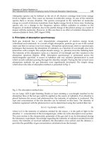
Fig. 3. Frequency responses of the R1, R2 and ReR resonators in transmitted-power regime
measured by a network analyzer. The resonance curves of the discussed modes are marked
The ordinary R1 resonator can be successfully replaced with the known type of TE
011
-mode
split-cylinder resonator (SCR) (Janezic & Baker-Jarvis 1999) – see Fig. 2c. It consists of two
equal cylindrical sections with diameter D
1
(as in CR1) and height H
1/2
= 0.5H
1
. The sample
with thickness h and arbitrary shape is placed into the radial gap between the cylinders. If
the sample has disk shape, its diameter D
S
should fit the SCR diameter D
1
with at least 10%
in reserve, i. e. D
s
1.1D
1
. The SCR resonator (as R1) is suitable for determination of the
longitudinal dielectric parameters –
’
||
, tan
||
. The presented in Fig. 6a SCR has the
following dimensions: D
1
= 30.00 mm, H
1
= 30.16 mm, and the TE
011
-mode resonance
parameters – f
0
SCR
= 13.1574 GHz, Q
0
SCR
= 8171. In spite of the lower Q-factor, the clear
advantage of SCR is the easier measurement procedure without preliminary sample cutting.
The radial SCR section must have big enough diameter (D
R
~ 1.5D
1
) in order to minimize the
parasitic lateral radiation even for thicker samples (see Dankov & Hadjistamov, 2007).
The considered pair of resonators (CR1&CR2) is not enough convenient for broadband
measurements of the anisotropy, even when a set of resonator pairs with different diameters
is being used. More suitable for this purpose is the pair of tunable resonators, shown in Fig.
4 and Fig. 6b. The split-coaxial resonator SCoaxR (see Dankov & Hadjistamov, 2007) can
successfully replace the ordinary fixed-size resonator R1 (or SCR), while the tunable re-
entrant resonator ReR (see Hadjistamov et. al., 2007) – the fixed-size resonator R2. The
SCoaxR is a variant of the split-cylinder resonator with a pair of top and bottom cylindrical
metal posts with height H
r
and diameter D
r
into the resonator body.
Fig. 4. Pair of tunable resonators: a) split-coaxial cylinder resonator SCoaxR as R1; b) re-
entrant resonator ReR as R2
sample
metal walls
h
H
1/2
D
r
D
R
a
H
r
R1: SCoaxR
D
1
D
2
D
r
H
r
b
R2: ReR
h
H
2
Fig. 5. Pair of split-post dielectric resonator SPDR: a) electrically-splitted resonator SPDR(e)
as R1; b) magnetically-splitted resonator SPDR(m) as R2; both with one DR
Fig. 6. Resonators’ photos of different pairs: a) R1, R2, SCR; b) ReR; ScoaxR; c) SPDR’s (e/m)
h
H
1/2
d
DR
D
R
a
h
DR
R1: SPDR(e)
D
1
b
R2: SPDR(m)
d
DR
h
DR
h
D
2
D
R
H
2
DR's
sample
metal walls
SCR
R2
disk samples
R2’
R1
SCoaxR
disk sample
sample
tuning metal
posts
ReR
sample
a
b
c
SPDR (m)
SPDR (e)
DR’s
DR
disk samples
sam
p
le
disk
sam
p
le
MicrowaveandMillimeterWaveTechnologies:
fromPhotonicBandgapDevicestoAntennaandApplications82
The adjustment of the resonance frequency is possible by changing of the height H
r
with
more than one octave below the resonance frequency of the hollow split-cylinder resonator.
The re-entrant resonator is a known low-frequency measurement structure. It has also an
inner metal cylinder with height H
r
and diameter D
r
. A problem of the reentrant and split-
coaxial measurement resonators is their lower unloaded Q factors (200-1500) compared to
these of the original cylinder resonators (3000-15000). In order to overcome this problem for
measurements at low frequency, a new pair of measurement resonators could be used
instead of R1 and R2 (see Fig. 5 and Fig. 6c): the split-post dielectric resonators SPDR (e/m)
with electric (e) or magnetic (m) type of splitting (e.g., see Baker-Jarvis et al., 1999) (in fact, a
non-split version of SPDR (m) is represented in Fig. 6c). The main novelty of this pair is the
inserted high-Q dielectric resonators DR’s that set different operating frequencies, lower
than the resonance frequencies in the ordinary cylinder resonators. The used DR’s should be
made by high-quality materials (sapphire, alumina, quartz, etc.) and this allows achieving of
unloaded Q factors about 5000-20000. A change in the frequency can be obtained by
replacement of a given DR with another one. DR’s with different shapes can be used:
cylinder, rectangular and ring. The DR’s dielectric constant should be not very high and not
very different from the sample dielectric constant to ensure an acceptable accuracy.
3.3 Modeling of the measurement structures
The accuracy of the dielectric anisotropy measurements directly depends upon the applied
theoretical model to the considered resonance structure. This model should ensure rigorous
relations between the measured resonance parameters (f
meas
, Q
meas
) and the substrate dielectric
parameters (
’
r
, tan
) along a given direction in dependence of the used resonance mode. The
simplest model is based on the perturbation approximation (e.g. Chen et al., 2004), but acceptable
results for anisotropy can be obtained only for very thin, low-K or foam materials (Ivanov &
Dankov, 2002). If the resonators have simple enough geometry (e.g. CR1, CR2), relatively
rigorous analytical models are possible to be constructed. Thus, accurate analytical models of the
simplest pair of fixed cylindrical cavity resonators R1&R2 are presented by Dankov, 2006
especially for determination of the dielectric anisotropy of multilayer materials (measurement
error less than 2-3% for dielectric constant anisotropy, and less than 8-10% – for the dielectric
loss tangent anisotropy. The relatively strong full-wave analytical models of the split-cylinder
resonator (Janezic & Baker-Jarvis, 1999) and split-post dielectric resonator (Krupka et al., 2001)
are also suitable for measurement purposes, but our experience shows, that the corresponding
models of the re-entrant resonator (Baker-Jarvis & Riddle, 1996) and the split-coaxial resonator
are not so accurate for measurement purposes. In order to increase the measurement accuracy,
we have developed the common principles for 3D modeling of resonance structures with
utilization of commercial 3D electromagnetic simulators as assistance tools for anisotropy
measurements (see Dankov et al., 2005, 2006; Dankov & Hadjistamov, 2007). The main principles
of this type of 3D modeling especially for measurement purposes with the presented two-
resonator method are described in §4. In our investigations we use Ansoft
®
HFSS simulator.
3.4 Measurement procedure and mode identifications
The procedure for dielectric anisotropy measurement of the prepared samples is as follows:
First of all, the resonance parameters (f
0meas
, Q
0meas
) of each empty resonator (without sample)
from the chosen pair should be accurately measured by Vector Network Analyzer VNA.
This step is very important for determination of the so-called "equivalent parameters" of
each resonator (see section 4.3); they should be introduced in the model of the resonator in
order to reduce the measurement errors. Then the resonance parameters (f
meas
, Q
meas
) of
each resonator with sample should be measured (for minimum 3-5 samples from each
substrate panel). This ensures well enough reproducibility for reliable determination of the
dielectric sample anisotropy with acceptable measurement errors (see section 4.4). The
identification of the mode of interest in the corresponding resonator from the pair is also an
important procedure. The simplest way is the preliminary simulation of the structure with
sample, which parameters are taken from the catalogue. This will give the approximate
position of the resonance curve. If the sample parameters are unknown, another way should
be used. For example, the mechanical construction of the exciting coaxial probes in the
resonators has to ensure rotating motion along the coaxial axis. Because the “pure” TE or
TM modes of interest in R1/R2 resonators have electric or magnetic field, strongly
orientated along one direction or in one plane (to be able to detect the sample anisotropy), a
simple rotation of the coaxial semi-loop orientation allows varying of the resonance curve
“height” and this will give the needed information about the excited mode type (TE or TM).
4. Measurement of Dielectric Anisotropy, Assisted by 3D Simulators
4.1 Main principles
The modern material characterization needs the utilization of powerful numerical tools for
obtaining of accurate results after modeling of very sophisticated measuring structures.
Such software tools can be the three-dimensional (3D) electromagnetic simulators, which
demonstrate serious capabilities in the modern RF design. Considering recent publications
in the area of material characterization, it is easy to establish that the 3D simulators have
been successfully applied for measurement purposes, too. The possibility to use commercial
frequency-domain simulators as assistant tools for accurate measurement of the substrate
anisotropy by the two-resonator method has been demonstrated by Dankov et al., 2005.
Then, this option is developed for the all types of considered resonators, following few
principles – simplicity, accuracy and fast simulations. Illustrative 3D models for some of
resonance structures, used in the two-resonator method (R1, R2 and SCR), are drawn in Fig.
7. Three main rules have been accepted to build these models for accurate and time-effective
processing of the measured resonance parameters – a stylized drawing of the resonator
body with equivalent diameters (D
1e
or D
2e
), an optimized number of line segments (N = 72-
180) for construction of the cylindrical surfaces and a suitable for the operating mode
splitting (1/4 or 1/8 from the whole resonator body), accompanied by appropriate
boundary conditions at the cut-off planes. Although the real resonators have the necessary
coupling elements, the resonator bodies can be introduced into the model as pure closed
cylinders and this approach allows applying the eigen-mode solver of the modern 3D
simulators (Ming et al., 2008). The utilization of the eigen-mode option for obtaining of the
resonance frequency and the unloaded Q-factor (notwithstanding that the modeled
resonator is not fully realistic) considerably facilitates the anisotropy measurement
procedure assisted by 3D simulators, if additionally equivalent parameters have been
introduced (see 4.3) and symmetrical resonator splitting (see 4.2) has been done.
DielectricAnisotropyofModernMicrowaveSubstrates 83
The adjustment of the resonance frequency is possible by changing of the height H
r
with
more than one octave below the resonance frequency of the hollow split-cylinder resonator.
The re-entrant resonator is a known low-frequency measurement structure. It has also an
inner metal cylinder with height H
r
and diameter D
r
. A problem of the reentrant and split-
coaxial measurement resonators is their lower unloaded Q factors (200-1500) compared to
these of the original cylinder resonators (3000-15000). In order to overcome this problem for
measurements at low frequency, a new pair of measurement resonators could be used
instead of R1 and R2 (see Fig. 5 and Fig. 6c): the split-post dielectric resonators SPDR (e/m)
with electric (e) or magnetic (m) type of splitting (e.g., see Baker-Jarvis et al., 1999) (in fact, a
non-split version of SPDR (m) is represented in Fig. 6c). The main novelty of this pair is the
inserted high-Q dielectric resonators DR’s that set different operating frequencies, lower
than the resonance frequencies in the ordinary cylinder resonators. The used DR’s should be
made by high-quality materials (sapphire, alumina, quartz, etc.) and this allows achieving of
unloaded Q factors about 5000-20000. A change in the frequency can be obtained by
replacement of a given DR with another one. DR’s with different shapes can be used:
cylinder, rectangular and ring. The DR’s dielectric constant should be not very high and not
very different from the sample dielectric constant to ensure an acceptable accuracy.
3.3 Modeling of the measurement structures
The accuracy of the dielectric anisotropy measurements directly depends upon the applied
theoretical model to the considered resonance structure. This model should ensure rigorous
relations between the measured resonance parameters (f
meas
, Q
meas
) and the substrate dielectric
parameters (
’
r
, tan
) along a given direction in dependence of the used resonance mode. The
simplest model is based on the perturbation approximation (e.g. Chen et al., 2004), but acceptable
results for anisotropy can be obtained only for very thin, low-K or foam materials (Ivanov &
Dankov, 2002). If the resonators have simple enough geometry (e.g. CR1, CR2), relatively
rigorous analytical models are possible to be constructed. Thus, accurate analytical models of the
simplest pair of fixed cylindrical cavity resonators R1&R2 are presented by Dankov, 2006
especially for determination of the dielectric anisotropy of multilayer materials (measurement
error less than 2-3% for dielectric constant anisotropy, and less than 8-10% – for the dielectric
loss tangent anisotropy. The relatively strong full-wave analytical models of the split-cylinder
resonator (Janezic & Baker-Jarvis, 1999) and split-post dielectric resonator (Krupka et al., 2001)
are also suitable for measurement purposes, but our experience shows, that the corresponding
models of the re-entrant resonator (Baker-Jarvis & Riddle, 1996) and the split-coaxial resonator
are not so accurate for measurement purposes. In order to increase the measurement accuracy,
we have developed the common principles for 3D modeling of resonance structures with
utilization of commercial 3D electromagnetic simulators as assistance tools for anisotropy
measurements (see Dankov et al., 2005, 2006; Dankov & Hadjistamov, 2007). The main principles
of this type of 3D modeling especially for measurement purposes with the presented two-
resonator method are described in §4. In our investigations we use Ansoft
®
HFSS simulator.
3.4 Measurement procedure and mode identifications
The procedure for dielectric anisotropy measurement of the prepared samples is as follows:
First of all, the resonance parameters (f
0meas
, Q
0meas
) of each empty resonator (without sample)
from the chosen pair should be accurately measured by Vector Network Analyzer VNA.
This step is very important for determination of the so-called "equivalent parameters" of
each resonator (see section 4.3); they should be introduced in the model of the resonator in
order to reduce the measurement errors. Then the resonance parameters (f
meas
, Q
meas
) of
each resonator with sample should be measured (for minimum 3-5 samples from each
substrate panel). This ensures well enough reproducibility for reliable determination of the
dielectric sample anisotropy with acceptable measurement errors (see section 4.4). The
identification of the mode of interest in the corresponding resonator from the pair is also an
important procedure. The simplest way is the preliminary simulation of the structure with
sample, which parameters are taken from the catalogue. This will give the approximate
position of the resonance curve. If the sample parameters are unknown, another way should
be used. For example, the mechanical construction of the exciting coaxial probes in the
resonators has to ensure rotating motion along the coaxial axis. Because the “pure” TE or
TM modes of interest in R1/R2 resonators have electric or magnetic field, strongly
orientated along one direction or in one plane (to be able to detect the sample anisotropy), a
simple rotation of the coaxial semi-loop orientation allows varying of the resonance curve
“height” and this will give the needed information about the excited mode type (TE or TM).
4. Measurement of Dielectric Anisotropy, Assisted by 3D Simulators
4.1 Main principles
The modern material characterization needs the utilization of powerful numerical tools for
obtaining of accurate results after modeling of very sophisticated measuring structures.
Such software tools can be the three-dimensional (3D) electromagnetic simulators, which
demonstrate serious capabilities in the modern RF design. Considering recent publications
in the area of material characterization, it is easy to establish that the 3D simulators have
been successfully applied for measurement purposes, too. The possibility to use commercial
frequency-domain simulators as assistant tools for accurate measurement of the substrate
anisotropy by the two-resonator method has been demonstrated by Dankov et al., 2005.
Then, this option is developed for the all types of considered resonators, following few
principles – simplicity, accuracy and fast simulations. Illustrative 3D models for some of
resonance structures, used in the two-resonator method (R1, R2 and SCR), are drawn in Fig.
7. Three main rules have been accepted to build these models for accurate and time-effective
processing of the measured resonance parameters – a stylized drawing of the resonator
body with equivalent diameters (D
1e
or D
2e
), an optimized number of line segments (N = 72-
180) for construction of the cylindrical surfaces and a suitable for the operating mode
splitting (1/4 or 1/8 from the whole resonator body), accompanied by appropriate
boundary conditions at the cut-off planes. Although the real resonators have the necessary
coupling elements, the resonator bodies can be introduced into the model as pure closed
cylinders and this approach allows applying the eigen-mode solver of the modern 3D
simulators (Ming et al., 2008). The utilization of the eigen-mode option for obtaining of the
resonance frequency and the unloaded Q-factor (notwithstanding that the modeled
resonator is not fully realistic) considerably facilitates the anisotropy measurement
procedure assisted by 3D simulators, if additionally equivalent parameters have been
introduced (see 4.3) and symmetrical resonator splitting (see 4.2) has been done.
MicrowaveandMillimeterWaveTechnologies:
fromPhotonicBandgapDevicestoAntennaandApplications84
Fig. 7. Equivalent 3D models of three resonators R1, R2 and SCR and boundary conditions
BC. BC legend: 1 – finite conductivity; 2 – E-field symmetry; 3 – H-field symmetry; 4 – perfect
H-wall (natural BC between two dielectrics); the BC over the all metal surface are 1)
4.2 Resonator splitting
In principle, the used modes in the measurement resonators for realization of the two-
resonator method have simple E-field distribution (parallel or perpendicular to the sample
surface). This specific circumstance allows accepting an important approach: not to simulate
the whole cylindrical cavities; but only just one symmetrical part of them: 1/8 from R1, SPR
and 1/4 from R2. Such approach requires suitable symmetrical boundary conditions to be
chosen, illustrated in Fig. 7. Two magnetic-wall boundary conditions should be accepted at
the split-resonator surfaces – “E-field symmetry” (if the E field is parallel to the surface) or
“H-field symmetry” (if the E field is perpendicular to the surface). The simulated resonance
parameters of the whole resonator (R1 or R2) and of its (1/8) or (1/4) equivalent practically
coincide for equal conditions; the differences are close to the measurement errors for the
frequency and the Q-factor (see data in Table 1). The utilization of the symmetrical cutting in
the 3D models instead of the whole resonator is a key assumption for the reasonable
application of the powerful 3D simulators for measurement purposes. This simple approach
solves three important simulation problems: 1) it considerably decreases the computational
time (up to 180 times for R1 and 50 times for R2); 2) allows increasing of the computational
accuracy and 3) suppresses the possible virtual excitation of non-physical modes during the
simulations in the whole resonator near to the modes of interest. The last circumstance is
very important. The finite number of surface segments in the full 3D model of the cavity in
combination with the finite-element mesh leads to a weak, but unavoidable structure
asymmetry and a number of parasitic resonances with close frequencies and different Q-
factors appear in the mode spectrum near to the symmetrical TE/TM modes of interest.
These parasitic modes fully disappear in the symmetrical (1/4)-R2 and (1/8)-R1 cavity
models, which makes the mode identification much easier (see the pictures in Fig. 8).
4.2 Equivalent resonator parameters
Usually, if an empty resonator has been measured and simulated with fixed dimensions, the
simulated and measured resonance parameters do not fully coincide, f
0sim
f
0meas
, Q
0sim
Q
0meas
. There are a lot of reasons for such a result – dimensions uncertainty, influence of the
coupling loops, tuning screws, eccentricity, surface cleanness and roughness, temperature
variation, etc.). In order to overcome this problem and due to the preliminary decision to
SCR
(1/8) SCR
1
4
R1
(1/8) R1
1
2
3
1
R2
1
2
1
(1/4) R2
1
2
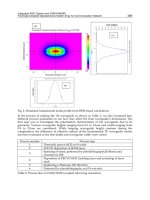
Fig. 8. Simulated electric-field E distribution (scalar and vector) in the considered pairs of
measurement resonators (as R1 or R2): a) cylinder resonators; b) tunable resonators; c)
SPDR’s. Presence of similar pictures makes the mode identification mush easier.
ignore the details and to construct pure stylized resonator model, the approach, based on
the introduction of equivalent parameters (dimensions and surface conductivity) becomes very
important. The idea is clear – the values of these parameters in the model have to be tuned
until a coincidence between the calculated and the measured resonance parameters is
achieved: f
0sim
~ f
0meas
, Q
0sim
~ Q
0meas
(~0.01-% coincidence is usually enough). The problem is
how to realize this approach? Let’s start with the simplest case – the equivalent 3D models
of the pair CR1/CR2 (Fig. 7). In this approach each 3D model is drown as a pure cylinder
with equivalent diameter D
eq1,2
(instead the geometrical one D
1,2
), actual height H
1,2
and
equivalent wall conductivity
eq1,2
of the empty resonators. The equivalent geometrical
parameter (D instead of H) is chosen on the base of simple principle: the variation of which
parameter influences most the resonance frequencies of the empty cavities CR1 and CR2?
1/8 R1
1/4 R2
1/8 SC (R1)
a
1/8 SCoaxR (R1)
1/4 Re (R2)
b
1/4 SPDR R2
1/4 SPDR R1
c
DielectricAnisotropyofModernMicrowaveSubstrates 85
Fig. 7. Equivalent 3D models of three resonators R1, R2 and SCR and boundary conditions
BC. BC legend: 1 – finite conductivity; 2 – E-field symmetry; 3 – H-field symmetry; 4 – perfect
H-wall (natural BC between two dielectrics); the BC over the all metal surface are 1)
4.2 Resonator splitting
In principle, the used modes in the measurement resonators for realization of the two-
resonator method have simple E-field distribution (parallel or perpendicular to the sample
surface). This specific circumstance allows accepting an important approach: not to simulate
the whole cylindrical cavities; but only just one symmetrical part of them: 1/8 from R1, SPR
and 1/4 from R2. Such approach requires suitable symmetrical boundary conditions to be
chosen, illustrated in Fig. 7. Two magnetic-wall boundary conditions should be accepted at
the split-resonator surfaces – “E-field symmetry” (if the E field is parallel to the surface) or
“H-field symmetry” (if the E field is perpendicular to the surface). The simulated resonance
parameters of the whole resonator (R1 or R2) and of its (1/8) or (1/4) equivalent practically
coincide for equal conditions; the differences are close to the measurement errors for the
frequency and the Q-factor (see data in Table 1). The utilization of the symmetrical cutting in
the 3D models instead of the whole resonator is a key assumption for the reasonable
application of the powerful 3D simulators for measurement purposes. This simple approach
solves three important simulation problems: 1) it considerably decreases the computational
time (up to 180 times for R1 and 50 times for R2); 2) allows increasing of the computational
accuracy and 3) suppresses the possible virtual excitation of non-physical modes during the
simulations in the whole resonator near to the modes of interest. The last circumstance is
very important. The finite number of surface segments in the full 3D model of the cavity in
combination with the finite-element mesh leads to a weak, but unavoidable structure
asymmetry and a number of parasitic resonances with close frequencies and different Q-
factors appear in the mode spectrum near to the symmetrical TE/TM modes of interest.
These parasitic modes fully disappear in the symmetrical (1/4)-R2 and (1/8)-R1 cavity
models, which makes the mode identification much easier (see the pictures in Fig. 8).
4.2 Equivalent resonator parameters
Usually, if an empty resonator has been measured and simulated with fixed dimensions, the
simulated and measured resonance parameters do not fully coincide, f
0sim
f
0meas
, Q
0sim
Q
0meas
. There are a lot of reasons for such a result – dimensions uncertainty, influence of the
coupling loops, tuning screws, eccentricity, surface cleanness and roughness, temperature
variation, etc.). In order to overcome this problem and due to the preliminary decision to
SCR
(1/8) SCR
1
4
R1
(1/8) R1
1
2
3
1
R2
1
2
1
(1/4) R2
1
2
Fig. 8. Simulated electric-field E distribution (scalar and vector) in the considered pairs of
measurement resonators (as R1 or R2): a) cylinder resonators; b) tunable resonators; c)
SPDR’s. Presence of similar pictures makes the mode identification mush easier.
ignore the details and to construct pure stylized resonator model, the approach, based on
the introduction of equivalent parameters (dimensions and surface conductivity) becomes very
important. The idea is clear – the values of these parameters in the model have to be tuned
until a coincidence between the calculated and the measured resonance parameters is
achieved: f
0sim
~ f
0meas
, Q
0sim
~ Q
0meas
(~0.01-% coincidence is usually enough). The problem is
how to realize this approach? Let’s start with the simplest case – the equivalent 3D models
of the pair CR1/CR2 (Fig. 7). In this approach each 3D model is drown as a pure cylinder
with equivalent diameter D
eq1,2
(instead the geometrical one D
1,2
), actual height H
1,2
and
equivalent wall conductivity
eq1,2
of the empty resonators. The equivalent geometrical
parameter (D instead of H) is chosen on the base of simple principle: the variation of which
parameter influences most the resonance frequencies of the empty cavities CR1 and CR2?
1/8 R1
1/4 R2
1/8 SC (R1)
a
1/8 SCoaxR (R1)
1/4 Re (R2)
b
1/4 SPDR R2
1/4 SPDR R1
c
MicrowaveandMillimeterWaveTechnologies:
fromPhotonicBandgapDevicestoAntennaandApplications86
Fig. 8. Dependencies of the normalized resonance frequency and normalized Q-factor of the
dominant mode in: a) resonators CR1/CR2; b) re-entrant resonator ReR, when one
geometrical parameter varies, while the other ones are fixed
Resonator type R1 (1/8) R1 R2 (1/4) R2
f
0 1,2
, GHz 13.1847 13.1846 12.6391 12.6391
Q
0 1,2
14088 14094 3459 3462
Computational time 177 : 1 47 : 1
Table 1. Resonance parameters of empty cavities and their equivalents (D
1
=30.0 mm; H
1
=
29.82 mm, D
2
=18.1 mm, H
2
= 12.09 mm)
N
72 108 144 180 216 288 Meas.
CR1 cavity (TE
011
mode): D
eq1
= 30.084 mm;
eq1
= 1.7010
7
S/m
f
01
, GHz 13.1578 13.1541 13.1529 13.1527 13.1523 13.1520 13.1528
Q
01
14086 14106 14115 14111 14108 14109 14117
CR2 cavity (TM
010
mode): D
eq2
= 18.156 mm;
eq2
= 0.9210
7
S/m
f
02
, GHz 12.6460 12.6418 12.6400 12.6392 12.6387 12.6383 12.6391
Q
02
3552 3475 3487 3533 3545 3571 3526
Table 2. Resonance parameters of empty cavities v/s the line-segment number N
0.90 0.95 1.00 1.05 1.10
0.94
0.96
0.98
1.00
1.02
1.04
1.06
CR2
CR1
f / f
0
D/D ,
H/H
0.90 0.95 1.00 1.05 1.10
0.94
0.96
0.98
1.00
1.02
1.04
1.06
CR2
CR1
; H1,2- vary; D1,2- fixed
; H1,2- fixed; D1,2- vary
Q / Q
0
D/D , H/H
a
0.90 0.95 1.00 1.05 1.10
0.8
0.9
1.0
1.1
1.2
ReR
D/D , H
r
/H
r
, D
r
/D
r
f / f
0
0.90 0.95 1.00 1.05 1.10
0.8
0.9
1.0
1.1
1.2
Hr- vary; Dr, D- fixed
Dr- vary; Hr, D- fixed
D- vary; Dr, Hr- fixed
Q / Q
0
D/D , H
r
/H
r
, D
r
/D
r
b
The reason for this assumption is given in Fig. 8, where the dependencies of the normalized
resonance frequencies and unloaded Q-factors are presented versus the relative dimension
variations. We can see that the diameter variation in both of the cavities affects the
resonance frequency stronger compared to the height variation. For example, in the case of
CR1 or SCR the increase of D
1
leads to 378 MHz/mm decrease of the resonance frequency
f
01
, while the increase of H
1
– only 64 MHz/mm decrease of f
01
. The effect over the Q-factor
in CR1 is similar, but in the case of CR2 the Q-factor changes due to the H
2
-variations are
stronger. Nevertheless, we accept the diameter as an equivalent parameter D
eq1,2
for the of
the cavities – see the concrete values in Table 2. We observe an increase of the equivalent
diameters with 0.3% in the both cases (D
eq1
~ 30.084 mm; D
eq2
= 18.156 mm), while for the
equivalent conductivity the obtained values are 3-4 times smaller (
eq1
= 1.7010
7
S/m;
eq2
=
0.92
10
7
S/m than the value of the bulk gold conductivity
Au
= 4.110
7
S/m). Thus, the
utilization of the equivalent cylindrical 3D models considerable decreases the measuring
errors, especially for determination of the loss tangent. Moreover, the equivalent model
takes into account the "daily" variations of the empty cavity parameters (±0.02% for D
eq1,2
;
±0.6% for
eq1,2
) and makes the proposed method for anisotropy measurement independent
of the equipment and the simulator used.
It is important to investigate the influence of the number N of surface segments necessary
for a proper approximation of the cylindrical resonator shape over the simulated resonance
characteristics. The data in Table 2 show that small numbers N < 144 does not fit well the
equivalent circle of the cylinders, while number N > 288 considerably increases the
computational time. The optimal values are in the range 144 < N < 216 for the both
resonators CR1 and CR2. The results show that the resonator CR2 is more sensitive to the N
value. The practical problem is –how to choose the right value N? We have found out that
the optimal value of N and the equivalent parameters D
eq
and
eq
are closely dependent.
Accurate and repeatable results are going to be achieved, if the following rule has been
accepted: the values of the equivalent parameters to be chosen from the simple expressions
(2, 3), and then to determine the suitable number N of surface segments in the models. The
needed expressions could be deduced from the analytical models (see Dankov, 2006):
2/1
2
1
2
0111
9.22468824.182 HfHR
eq
,
022
/74274.114 fR
eq
,
(2)
2
2,12,012,1
842.3947
Seq
Rf
,
(3)
where the surface resistance R
S1,2
is expressed as
1
2
011
5
11
01
3
01
2
11
5
1
)(109918.21/5.0
1
108798.1
fRRH
Q
fRHR
eqeqeqS
,
(4)
1
2202
5
02
2
222
/11056313.5
1
/40483.25.0
eqeqS
RHf
Q
RHR
(5)
All the geometrical dimensions R
eq1,2
and H
1,2
in the expressions (2-5) are in mm, f
01,2
– in
GHz, R
S1,2
– in Ohms and
eq1,2
– in S/m. After the described procedure, the optimal number
N of rectangular segments in CR1/CR2 is N ~ 144-180. Similar values can be obtained by a
simple rule – the line-segment width should be smaller than
/16 (
– wavelength). This
simple rule allows choosing of the right N value directly, without preliminary calculations.
DielectricAnisotropyofModernMicrowaveSubstrates 87
Fig. 8. Dependencies of the normalized resonance frequency and normalized Q-factor of the
dominant mode in: a) resonators CR1/CR2; b) re-entrant resonator ReR, when one
geometrical parameter varies, while the other ones are fixed
Resonator type R1 (1/8) R1 R2 (1/4) R2
f
0 1,2
, GHz 13.1847 13.1846 12.6391 12.6391
Q
0 1,2
14088 14094 3459 3462
Computational time 177 : 1 47 : 1
Table 1. Resonance parameters of empty cavities and their equivalents (D
1
=30.0 mm; H
1
=
29.82 mm, D
2
=18.1 mm, H
2
= 12.09 mm)
N
72 108 144 180 216 288 Meas.
CR1 cavity (TE
011
mode): D
eq1
= 30.084 mm;
eq1
= 1.7010
7
S/m
f
01
, GHz 13.1578 13.1541 13.1529 13.1527 13.1523 13.1520 13.1528
Q
01
14086 14106 14115 14111 14108 14109 14117
CR2 cavity (TM
010
mode): D
eq2
= 18.156 mm;
eq2
= 0.9210
7
S/m
f
02
, GHz 12.6460 12.6418 12.6400 12.6392 12.6387 12.6383 12.6391
Q
02
3552 3475 3487 3533 3545 3571 3526
Table 2. Resonance parameters of empty cavities v/s the line-segment number N
0.90 0.95 1.00 1.05 1.10
0.94
0.96
0.98
1.00
1.02
1.04
1.06
CR2
CR1
f / f
0
D/D ,
H/H
0.90 0.95 1.00 1.05 1.10
0.94
0.96
0.98
1.00
1.02
1.04
1.06
CR2
CR1
; H1,2- vary; D1,2- fixed
; H1,2- fixed; D1,2- vary
Q / Q
0
D/D , H/H
a
0.90 0.95 1.00 1.05 1.10
0.8
0.9
1.0
1.1
1.2
ReR
D/D , H
r
/H
r
, D
r
/D
r
f / f
0
0.90 0.95 1.00 1.05 1.10
0.8
0.9
1.0
1.1
1.2
Hr- vary; Dr, D- fixed
Dr- vary; Hr, D- fixed
D- vary; Dr, Hr- fixed
Q / Q
0
D/D , H
r
/H
r
, D
r
/D
r
b
The reason for this assumption is given in Fig. 8, where the dependencies of the normalized
resonance frequencies and unloaded Q-factors are presented versus the relative dimension
variations. We can see that the diameter variation in both of the cavities affects the
resonance frequency stronger compared to the height variation. For example, in the case of
CR1 or SCR the increase of D
1
leads to 378 MHz/mm decrease of the resonance frequency
f
01
, while the increase of H
1
– only 64 MHz/mm decrease of f
01
. The effect over the Q-factor
in CR1 is similar, but in the case of CR2 the Q-factor changes due to the H
2
-variations are
stronger. Nevertheless, we accept the diameter as an equivalent parameter D
eq1,2
for the of
the cavities – see the concrete values in Table 2. We observe an increase of the equivalent
diameters with 0.3% in the both cases (D
eq1
~ 30.084 mm; D
eq2
= 18.156 mm), while for the
equivalent conductivity the obtained values are 3-4 times smaller (
eq1
= 1.7010
7
S/m;
eq2
=
0.92
10
7
S/m than the value of the bulk gold conductivity
Au
= 4.110
7
S/m). Thus, the
utilization of the equivalent cylindrical 3D models considerable decreases the measuring
errors, especially for determination of the loss tangent. Moreover, the equivalent model
takes into account the "daily" variations of the empty cavity parameters (±0.02% for D
eq1,2
;
±0.6% for
eq1,2
) and makes the proposed method for anisotropy measurement independent
of the equipment and the simulator used.
It is important to investigate the influence of the number N of surface segments necessary
for a proper approximation of the cylindrical resonator shape over the simulated resonance
characteristics. The data in Table 2 show that small numbers N < 144 does not fit well the
equivalent circle of the cylinders, while number N > 288 considerably increases the
computational time. The optimal values are in the range 144 < N < 216 for the both
resonators CR1 and CR2. The results show that the resonator CR2 is more sensitive to the N
value. The practical problem is –how to choose the right value N? We have found out that
the optimal value of N and the equivalent parameters D
eq
and
eq
are closely dependent.
Accurate and repeatable results are going to be achieved, if the following rule has been
accepted: the values of the equivalent parameters to be chosen from the simple expressions
(2, 3), and then to determine the suitable number N of surface segments in the models. The
needed expressions could be deduced from the analytical models (see Dankov, 2006):
2/1
2
1
2
0111
9.22468824.182 HfHR
eq
,
022
/74274.114 fR
eq
,
(2)
2
2,12,012,1
842.3947
Seq
Rf
,
(3)
where the surface resistance R
S1,2
is expressed as
1
2
011
5
11
01
3
01
2
11
5
1
)(109918.21/5.0
1
108798.1
fRRH
Q
fRHR
eqeqeqS
,
(4)
1
2202
5
02
2
222
/11056313.5
1
/40483.25.0
eqeqS
RHf
Q
RHR
(5)
All the geometrical dimensions R
eq1,2
and H
1,2
in the expressions (2-5) are in mm, f
01,2
– in
GHz, R
S1,2
– in Ohms and
eq1,2
– in S/m. After the described procedure, the optimal number
N of rectangular segments in CR1/CR2 is N ~ 144-180. Similar values can be obtained by a
simple rule – the line-segment width should be smaller than
/16 (
– wavelength). This
simple rule allows choosing of the right N value directly, without preliminary calculations.
MicrowaveandMillimeterWaveTechnologies:
fromPhotonicBandgapDevicestoAntennaandApplications88
Let’s now to consider the determination of the equivalent parameters in the other types of
resonators. In Fig. 8b we demonstrate the influence of the relative shift of each of the
dimensions D, D
r
and H
r
over the normalized resonance parameters f/f
0
and Q/Q
0
of an
empty re-entrant cavity. The results show that the resonance frequency variations are
strongest due to the variations of the re-entrant cylinder height H
r
(10% for H
r
/H
r
~ 5%).
Therefore, it should be chosen as an equivalent parameter in the 3D model of the re-entrant
cavity (equivalent height). But the variations due to the outer diameter are also strong (5%
for D/D ~ 5%) (For build-in cylinder diameter the changes are smaller than 1% for
D
r
/D
r
~ 5%). The variations of the Q-factor of the dominant mode have similar values for
all of the considered parameters (note: the effects for H
r
/H
r
and for D/D have opposite
signs). So, in the re-entrant cavity 3D model we can select two equivalent geometrical
parameters: 1) equivalent outer cylinder diameter D
eq2
, when H
r
= 0 (e. g. the re-entrant
resonator is a pure cylindrical resonator with TM
010
mode) and 2) equivalent build-in
cylinder height H
eq_r
, when D
eq2
has been already chosen. This approximation allows us a
direct comparison between the results from cylindrical and re-entrant resonators, if the last
one has a movable inner cylinder. Very similar behaviour has the other tunable cavity
SCoaxR – we have to determine an equivalent height H
eq_r
of the both coaxial cylinders.
The last pair of measurement resonators consists of additional unknown elements – one or
two DR’s. In this more complicated case, after the determination of the mentioned
equivalent parameters of the empty resonance cavity (R1, SCR or R2), an “equivalent dielectric
resonator” should be introduced. This includes the determination of the actual dielectric
parameters (
’
DR
, tan
DR
) of the DR with measured dimensions d
DR
and h
DR
. The anisotropy
of the DR itself is not a problem in our model; in fact, we determine exactly the actual
parameters in the corresponding case – parallel ones in SPDR (e) or perpendicular ones in
SPDR(m).The actual parameters of the necessary supporting elements (rod, disk) for the DR
mounting should also to be determined. The only problem is the “depolarization effect”,
which takes place in similar structures with relatively big normal components of the electric
field at the interfaces between two dielectrics. In our 3D models the presence of
depolarization effects are hidden (more or less) into the parameters of the “equivalent DR”.
4.4 Measurement errors, sensitivity and selectivity
The investigation of the sources of measurement errors during the substrate-anisotropy
determination by the two-resonator method is very important for its applicability. The
analysis can be done with the help of the 3D equivalent model of a given structure: the value
of one parameter has to be varied (e. g. sample height) keeping the values of all other
parameters and thus, the particular relative variation of the permittivity and loss tangent
values can be calculated. Finally, the total relative measurement error is estimated as a sum
of these particular relative variations. A relatively full error analysis was done by Dankov,
2006 for ordinary resonators CR1/CR2. It was shown that the contributions of the separate
parameter variations are very different, but the introduction of the equivalent parameters –
equivalent D
eq1,2
, equivalent height H
eq_r
(in ReR and SCoaxR) and equivalent conductivity
eq1,2
, considerably reduce the dielectric anisotropy uncertainty due to the uncertainty of the
resonator parameters. Thus, the main benefit of the utilization of equivalent 3D models is
that the errors for the measurement of the pairs of values (
’
||
, tan
||
) and (
’
, tan
)
remain to depend mainly on the uncertainty h/h in the sample height (Fig. 9), especially
for relative thin sample, and weakly on the sample positioning uncertainty (in CR1).
Fig. 9. Calculated relative errors in CR1/CR2:
’/
’ v/s h/h and tan
/tan
v/s Q
0
/Q
0
Fig. 10. Calculated sensitivity in CR1/CR2 according to sample dielectric constants
’
||
,
’
Taking into account the above-discussed issues the measuring errors in the two-resonator
method can be estimated as follows: < 1.0-1.5 % for
’
||
and < 5 % for
’
for a relatively thin
substrate like RO3203 with thickness h = 0.254 mm measured with errors h/h < 2% (this is
the main source of measurement errors for the permittivity). Besides, if the positioning
uncertainty reaches a value of 10 % for the sample positioning in CR1 (absolute shift up to
1.5 mm), the relative measurement error of
’
||
does not exceed the value of 2.5 %. The
measuring errors for the determination of the dielectric loss tangent are estimated as: 5-7 %
for tan
||
, but up to 25 % for tan
, when the measuring error for the unloaded Q-factor is
5 % (this is the main additional source for the loss-tangent errors; the other one is the
dielectric constant error).
A real problem of the considered method for the determination of the dielectric constant
anisotropy A
is the measurement sensitivity of the TM
010
mode in the resonator CR2 (for '
),
which is noticeably smaller compared to the sensitivity of the TE
011
mode in CR1 (for
’
||
).
We illustrate this effect in Fig. 10, where the curves of the resonance frequency shift versus
the dielectric constant have been presented for one-layer samples with height h from 0.125
up to 4 mm. The shift f/ in R1 for a sample with h = 0.5 mm leads to a decrease of 480
MHz for the doubling of
’
||
(from 2 to 4), while the corresponding shift in CR2 leads only
to a decrease of 42.9 MHz for the doubling of '
. Also, the Q-factor of the TM
010
mode in
CR2 is smaller compared to the Q-factor of the TE
011
mode in CR1. This leads to an unequal
accuracy for the determination of the loss tangent anisotropy A
tan
, too.
0.01 0.1 1 10
0
5
10
15
20
' /
' , %
tan
/tan
, %
h / h, %
Q
0
/ Q
0
, %
TE
011
mode (CR1)
TM
010
mode (CR2)
2 4 6 8
0.85
0.90
0.95
1.00
2 4 6 8 10
TM
010
mode (CR2)
TE
011
mode (CR1)
'
||
h = 0.125 mm
0.25 mm
0.5 mm
1.0 mm
1.5 mm
'
f (
) / f (1)
DielectricAnisotropyofModernMicrowaveSubstrates 89
Let’s now to consider the determination of the equivalent parameters in the other types of
resonators. In Fig. 8b we demonstrate the influence of the relative shift of each of the
dimensions D, D
r
and H
r
over the normalized resonance parameters f/f
0
and Q/Q
0
of an
empty re-entrant cavity. The results show that the resonance frequency variations are
strongest due to the variations of the re-entrant cylinder height H
r
(10% for H
r
/H
r
~ 5%).
Therefore, it should be chosen as an equivalent parameter in the 3D model of the re-entrant
cavity (equivalent height). But the variations due to the outer diameter are also strong (5%
for D/D ~ 5%) (For build-in cylinder diameter the changes are smaller than 1% for
D
r
/D
r
~ 5%). The variations of the Q-factor of the dominant mode have similar values for
all of the considered parameters (note: the effects for H
r
/H
r
and for D/D have opposite
signs). So, in the re-entrant cavity 3D model we can select two equivalent geometrical
parameters: 1) equivalent outer cylinder diameter D
eq2
, when H
r
= 0 (e. g. the re-entrant
resonator is a pure cylindrical resonator with TM
010
mode) and 2) equivalent build-in
cylinder height H
eq_r
, when D
eq2
has been already chosen. This approximation allows us a
direct comparison between the results from cylindrical and re-entrant resonators, if the last
one has a movable inner cylinder. Very similar behaviour has the other tunable cavity
SCoaxR – we have to determine an equivalent height H
eq_r
of the both coaxial cylinders.
The last pair of measurement resonators consists of additional unknown elements – one or
two DR’s. In this more complicated case, after the determination of the mentioned
equivalent parameters of the empty resonance cavity (R1, SCR or R2), an “equivalent dielectric
resonator” should be introduced. This includes the determination of the actual dielectric
parameters (
’
DR
, tan
DR
) of the DR with measured dimensions d
DR
and h
DR
. The anisotropy
of the DR itself is not a problem in our model; in fact, we determine exactly the actual
parameters in the corresponding case – parallel ones in SPDR (e) or perpendicular ones in
SPDR(m).The actual parameters of the necessary supporting elements (rod, disk) for the DR
mounting should also to be determined. The only problem is the “depolarization effect”,
which takes place in similar structures with relatively big normal components of the electric
field at the interfaces between two dielectrics. In our 3D models the presence of
depolarization effects are hidden (more or less) into the parameters of the “equivalent DR”.
4.4 Measurement errors, sensitivity and selectivity
The investigation of the sources of measurement errors during the substrate-anisotropy
determination by the two-resonator method is very important for its applicability. The
analysis can be done with the help of the 3D equivalent model of a given structure: the value
of one parameter has to be varied (e. g. sample height) keeping the values of all other
parameters and thus, the particular relative variation of the permittivity and loss tangent
values can be calculated. Finally, the total relative measurement error is estimated as a sum
of these particular relative variations. A relatively full error analysis was done by Dankov,
2006 for ordinary resonators CR1/CR2. It was shown that the contributions of the separate
parameter variations are very different, but the introduction of the equivalent parameters –
equivalent D
eq1,2
, equivalent height H
eq_r
(in ReR and SCoaxR) and equivalent conductivity
eq1,2
, considerably reduce the dielectric anisotropy uncertainty due to the uncertainty of the
resonator parameters. Thus, the main benefit of the utilization of equivalent 3D models is
that the errors for the measurement of the pairs of values (
’
||
, tan
||
) and (
’
, tan
)
remain to depend mainly on the uncertainty h/h in the sample height (Fig. 9), especially
for relative thin sample, and weakly on the sample positioning uncertainty (in CR1).
Fig. 9. Calculated relative errors in CR1/CR2:
’/
’ v/s h/h and tan
/tan
v/s Q
0
/Q
0
Fig. 10. Calculated sensitivity in CR1/CR2 according to sample dielectric constants
’
||
,
’
Taking into account the above-discussed issues the measuring errors in the two-resonator
method can be estimated as follows: < 1.0-1.5 % for
’
||
and < 5 % for
’
for a relatively thin
substrate like RO3203 with thickness h = 0.254 mm measured with errors h/h < 2% (this is
the main source of measurement errors for the permittivity). Besides, if the positioning
uncertainty reaches a value of 10 % for the sample positioning in CR1 (absolute shift up to
1.5 mm), the relative measurement error of
’
||
does not exceed the value of 2.5 %. The
measuring errors for the determination of the dielectric loss tangent are estimated as: 5-7 %
for tan
||
, but up to 25 % for tan
, when the measuring error for the unloaded Q-factor is
5 % (this is the main additional source for the loss-tangent errors; the other one is the
dielectric constant error).
A real problem of the considered method for the determination of the dielectric constant
anisotropy A
is the measurement sensitivity of the TM
010
mode in the resonator CR2 (for '
),
which is noticeably smaller compared to the sensitivity of the TE
011
mode in CR1 (for
’
||
).
We illustrate this effect in Fig. 10, where the curves of the resonance frequency shift versus
the dielectric constant have been presented for one-layer samples with height h from 0.125
up to 4 mm. The shift f/ in R1 for a sample with h = 0.5 mm leads to a decrease of 480
MHz for the doubling of
’
||
(from 2 to 4), while the corresponding shift in CR2 leads only
to a decrease of 42.9 MHz for the doubling of '
. Also, the Q-factor of the TM
010
mode in
CR2 is smaller compared to the Q-factor of the TE
011
mode in CR1. This leads to an unequal
accuracy for the determination of the loss tangent anisotropy A
tan
, too.
0.01 0.1 1 10
0
5
10
15
20
' /
' , %
tan
/tan
, %
h / h, %
Q
0
/ Q
0
, %
TE
011
mode (CR1)
TM
010
mode (CR2)
2 4 6 8
0.85
0.90
0.95
1.00
2 4 6 8 10
TM
010
mode (CR2)
TE
011
mode (CR1)
'
||
h = 0.125 mm
0.25 mm
0.5 mm
1.0 mm
1.5 mm
'
f (
) / f (1)
MicrowaveandMillimeterWaveTechnologies:
fromPhotonicBandgapDevicestoAntennaandApplications90
Fig. 11. Dependencies of the normalized resonance frequency and Q-factors of the resonance
modes for anisotropic and isotropic samples: a) v/s dielectric anisotropy A
, A
tan
; b) v/s
the substrate thickness h
Thus, the measured anisotropy for the dielectric constant A
< 2.5-3 % and for the dielectric loss
tangent A
tan
< 10-12 % can be associated to a practical isotropy of the sample (
’
||
’
; tan
||
tan
), because these differences fall into the measurement error margins.
Finally, the problem of the resonator selectivity (the ability to measure either pure parallel or pure
perpendicular components of the dielectric parameters) is considered. The results for the
normalized dependencies of the resonance frequencies and Q-factors for anisotropic and
isotropic samples in the separate resonators are presented in Fig. 11. These are two types of
dependencies– according to the substrate anisotropy at a fixed thickness and according to the
substrate thickness at a fixed anisotropy. How have these data been obtained? Each 3D model of
the considered resonators contains sample with fixed dielectric parameters: once isotropic, then –
anisotropic. The models in these two cases have been simulated and the obtained resonance
frequencies and Q-factors are compared – as ratio (f, Q)
anisotropic
/(f, Q)
isotropic
. The presented results
unambiguously show that most of the used resonators measure the corresponding “pure”
parameters with errors less than 0.3-0.4 % for dielectric constant and less than 0.5-1.0 % for the
dielectric loss tangent in a wide range of anisotropy and substrate thickness. The problems
appear mainly in the SCR; so the split-cylinder resonator can be used neither for big dielectric
anisotropy, nor for thick samples – its selectivity becomes considerably smaller compared to the
good selectivity of the rest of the resonators. A problem appears also for the measurement of the
dielectric loss tangent in very thick samples by CR2 resonator (see Fig. 11b).
-20 -10 0 10 20
0.990
0.995
1.000
1.005
1.010
1.015
1.020
CR1
CR2
ReR
SCR
SCoaxR
f
anisotropy
/ f
isotropy
A
, %
-20 -10 0 10 20
0.92
0.96
1.00
1.04
1.08
h = 1.5 mm
Q
anisotropic
/ Q
isotropic
A
tan
, %
0 1 2 3 4
0.980
0.985
0.990
0.995
1.000
CR1
CR2
ReR
SCR
f
anisotropic
/ f
isotropic
h , mm
0 1 2 3 4
0.900
0.925
0.950
0.975
1.000
A
= 7.7%
A
tan
= 25.2%
Q
anisotropic
/ Q
isotropic
h , mm
a
b
5. Data for the Anisotropy of Same Popular Dielectric Substrates
5.1 Isotropic material test
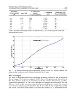
A natural test for the two-resonator method and the proposed equivalent 3D models is the
determination of the dielectric isotropy of clearly expressed isotropic materials (“isotropic-
sample“ test). Results for for three types of isotropic materials have been presented in Table
3 with increased values of dielectric constant and loss tangent – PTFE, polyolefine and
polycarbonate (averaged for 5 samples). The measured “anisotropy” by the pair of
resonators CR1/CR2 is very small (< 0.6 % for the dielectric constant and < 4% for the loss
tangent) – i. e. the practical isotropy of these materials is obvious. The next “isotropic-
sample” test is for polycarbonate samples with increased thickness (from 0.5 to 3 mm) – Fig.
12. The both resonators give close values for the dielectric constant (measured average value
’
r
~2.6525) even for thick samples, nevertheless that the “anisotropy” A
reaches to the
value ~2.5 %. The results for the loss tangent are similar – the models give average tan
0.005-0.0055 and mean “anisotropy” A
tan
< 4%. All these differences correspond to the
practical isotropy of the considered material, especially for small thickness h < 1.5 mm. The
final test is for one sample – 0.51-mm thick transparent polycarbonate Lexan
®
D-sheet (
r
2.9; tan
0.0065 at 1 MHz), measured by different resonators in wide frequency range 2-18
GHz. The measured “anisotropy” of this material is less than 3 % for A
and less than 11 %
for A
tan
. These values should be considered as an expression of the limited ability of the
two-resonator method to detect an ideal isotropy, as well as a possible small anisotropy of
microwave materials with relatively small thickness (h < 2 mm).
Fig. 12. Isotropy test for polycarbonate sheets: a) v/s the thickness h; b) v/s the frequency
a
0.5 1.0 1.5 2.0 2.5 3.0
2.68
2.70
2.72
2.74
2.76
2.78
2.80
2.82
10-12 GHz
~2.5 %
A
< 0.12 %
'
'
'
r
h, mm
0.5 1.0 1.5 2.0 2.5 3.0
0.00450
0.00475
0.00500
0.00525
0.00550
0.00575
0.00600
Polycarbonate
~4.5 %
A
tan
~ 0.9 %
tan
tan
tan
h, mm
b
0 2 4 6 8 10 12 14 16 18 20
0.005
0.006
0.007
Polycarbonate (h = 0.51 mm)
tan
f , GHz
0 2 4 6 8 10 12 14 16 18 20
2.4
2.5
2.6
2.7
2.8
2.9
3.0
CR1
SCR
SCoaxR
SDPR(e)
CR2
ReR
SDPR(m)
cataloque
'
r
f , GHz
DielectricAnisotropyofModernMicrowaveSubstrates 91
Fig. 11. Dependencies of the normalized resonance frequency and Q-factors of the resonance
modes for anisotropic and isotropic samples: a) v/s dielectric anisotropy A
, A
tan
; b) v/s
the substrate thickness h
Thus, the measured anisotropy for the dielectric constant A
< 2.5-3 % and for the dielectric loss
tangent A
tan
< 10-12 % can be associated to a practical isotropy of the sample (
’
||
’
; tan
||
tan
), because these differences fall into the measurement error margins.
Finally, the problem of the resonator selectivity (the ability to measure either pure parallel or pure
perpendicular components of the dielectric parameters) is considered. The results for the
normalized dependencies of the resonance frequencies and Q-factors for anisotropic and
isotropic samples in the separate resonators are presented in Fig. 11. These are two types of
dependencies– according to the substrate anisotropy at a fixed thickness and according to the
substrate thickness at a fixed anisotropy. How have these data been obtained? Each 3D model of
the considered resonators contains sample with fixed dielectric parameters: once isotropic, then –
anisotropic. The models in these two cases have been simulated and the obtained resonance
frequencies and Q-factors are compared – as ratio (f, Q)
anisotropic
/(f, Q)
isotropic
. The presented results
unambiguously show that most of the used resonators measure the corresponding “pure”
parameters with errors less than 0.3-0.4 % for dielectric constant and less than 0.5-1.0 % for the
dielectric loss tangent in a wide range of anisotropy and substrate thickness. The problems
appear mainly in the SCR; so the split-cylinder resonator can be used neither for big dielectric
anisotropy, nor for thick samples – its selectivity becomes considerably smaller compared to the
good selectivity of the rest of the resonators. A problem appears also for the measurement of the
dielectric loss tangent in very thick samples by CR2 resonator (see Fig. 11b).
-20 -10 0 10 20
0.990
0.995
1.000
1.005
1.010
1.015
1.020
CR1
CR2
ReR
SCR
SCoaxR
f
anisotropy
/ f
isotropy
A
, %
-20 -10 0 10 20
0.92
0.96
1.00
1.04
1.08
h = 1.5 mm
Q
anisotropic
/ Q
isotropic
A
tan
, %
0 1 2 3 4
0.980
0.985
0.990
0.995
1.000
CR1
CR2
ReR
SCR
f
anisotropic
/ f
isotropic
h , mm
0 1 2 3 4
0.900
0.925
0.950
0.975
1.000
A
= 7.7%
A
tan
= 25.2%
Q
anisotropic
/ Q
isotropic
h , mm
a
b
5. Data for the Anisotropy of Same Popular Dielectric Substrates
5.1 Isotropic material test
A natural test for the two-resonator method and the proposed equivalent 3D models is the
determination of the dielectric isotropy of clearly expressed isotropic materials (“isotropic-
sample“ test). Results for for three types of isotropic materials have been presented in Table
3 with increased values of dielectric constant and loss tangent – PTFE, polyolefine and
polycarbonate (averaged for 5 samples). The measured “anisotropy” by the pair of
resonators CR1/CR2 is very small (< 0.6 % for the dielectric constant and < 4% for the loss
tangent) – i. e. the practical isotropy of these materials is obvious. The next “isotropic-
sample” test is for polycarbonate samples with increased thickness (from 0.5 to 3 mm) – Fig.
12. The both resonators give close values for the dielectric constant (measured average value
’
r
~2.6525) even for thick samples, nevertheless that the “anisotropy” A
reaches to the
value ~2.5 %. The results for the loss tangent are similar – the models give average tan
0.005-0.0055 and mean “anisotropy” A
tan
< 4%. All these differences correspond to the
practical isotropy of the considered material, especially for small thickness h < 1.5 mm. The
final test is for one sample – 0.51-mm thick transparent polycarbonate Lexan
®
D-sheet (
r
2.9; tan
0.0065 at 1 MHz), measured by different resonators in wide frequency range 2-18
GHz. The measured “anisotropy” of this material is less than 3 % for A
and less than 11 %
for A
tan
. These values should be considered as an expression of the limited ability of the
two-resonator method to detect an ideal isotropy, as well as a possible small anisotropy of
microwave materials with relatively small thickness (h < 2 mm).
Fig. 12. Isotropy test for polycarbonate sheets: a) v/s the thickness h; b) v/s the frequency
a
0.5 1.0 1.5 2.0 2.5 3.0
2.68
2.70
2.72
2.74
2.76
2.78
2.80
2.82
10-12 GHz
~2.5 %
A
< 0.12 %
'
'
'
r
h, mm
0.5 1.0 1.5 2.0 2.5 3.0
0.00450
0.00475
0.00500
0.00525
0.00550
0.00575
0.00600
Polycarbonate
~4.5 %
A
tan
~ 0.9 %
tan
tan
tan
h, mm
b
0 2 4 6 8 10 12 14 16 18 20
0.005
0.006
0.007
Polycarbonate (h = 0.51 mm)
tan
f , GHz
0 2 4 6 8 10 12 14 16 18 20
2.4
2.5
2.6
2.7
2.8
2.9
3.0
CR1
SCR
SCoaxR
SDPR(e)
CR2
ReR
SDPR(m)
cataloque
'
r
f , GHz
MicrowaveandMillimeterWaveTechnologies:
fromPhotonicBandgapDevicestoAntennaandApplications92
Isotropic
Sample
h, mm
CR1:
f
1
, GHz/Q
1
’
||
/tan
||
CR2:
f
2
, GHz/Q
2
’
/ tan
“Anisotropy”
A
/A
tan
%
PTFE 0.945 12.6945/9596 2.0451/0.00025
12.3499/3160 2.0470/0.00026
-0.1 / -4.0
Polyolefine 0.7725 12.5856/8004 2.3060/0.00415
12.3756/3120 2.3210/0.00400
-0.6 / 3.7
Polycarbonate
1.000 12.3222/775 2.7712/0.00530
12.2325/1767 2.7650/0.00551
0.2 / -4.0
Table 3. “Isotropic-sample test” of the pair CR1/CR2. Cavity parameters: CR1: f
01
= 13.1512
GHz; Q
01
= 14154; D
eq1
= 30.088 mm;
eq1
= 1.71 10
7
S/m; CR2: f
02
= 12.6394 GHz; Q
02
=
3465; D
eq2
= 18.156 mm;
eq2
= 0.89 10
7
S/m
5.2 Data for some popular PWB substrates
The first example for anisotropic materials includes data for the measured dielectric
parameters of several commercial reinforced substrates with practically equal catalogue
parameters. These artificial materials contain different numbers of penetrated layers
(depending on the substrate thickness) of woven glass with an appropriate filling and
therefore, they may have more or less noticeable anisotropy. In fact, the catalogue data do
not include an information about the actual values of A
and A
tan
.
The measured results are presented in Table 4 for several RF substrates with thickness about
0.51 mm (20 mils) with catalogue dielectric constant ~3.38 and dielectric loss tangent ~0.0025
-0.0030, obtained by IPC TM-650 2.5.5.5 test method at 10 GHz. The substrates are presented
with their authentic designations and with their actual thickness h. We compare all the
measured resonance parameters (resonance frequency and Q-factor) by the pair CR1/CR2
and the forth dielectric parameters. A separate column in Table 4 contains the important
information about the measured anisotropy A
and A
tan
. The dielectric parameters are
averaged for minimum 5 samples, extracted from one substrate panel with controlled
producer’s origin. The measurement errors are: (
’/
’)
||
0.3%; (
’/
’)
0.5%; (tan
/
tan
)
||
1.2%; (tan
/tan
)
3%; for (f
/f
) 0.04%; (Q
/Q
) 1.5%; (h/h) 0.5%.
Nevertheless, that the substrates are offered as similar ones, they demonstrate different
measured parameters and anisotropy, which takes places mainly due to the variations in the
longitudinal (parallel) values
’
||
and tan
||
, obtained by CR1 and not included in the
catalogues. The measured transversal (normal) values
’
and tan
, obtained by CR2, differ
Substrate
(20mills thick)
h, mm
CR1:
f
1
, GHz/Q
1
’
||
/tan
||
CR2:
f
2
, GHz/Q
2
’
/ tan
A
/
A
tan
,%
IPC TM 650
2.5.5.5
@ 10 GHz
Rogers Ro4003
0.510
12.5050/1780
3.67/0.0037
12.4235/2834
3.38/0.0028
8.2/27.7
3.38/0.0027
Arlon 25N
0.520
12.5254/1492
3.57/0.0041
12.4243/2671
3.37/0.0033
5.8/21.6
3.38/0.0025
Isola 680
0.525
12.4820/1280
3.71/0.0049
12.4215/1767
3.32/0.0042
11.1/15.4
3.38/0.003
Taconic RF-35
0.512
12.4552/1176
3.90/0.0049
12.4254/2729
3.45/0.0038
12.2/25.3
3.50/0.0033
Neltec NH9338
0.520
12.4062/1171
4.02/0.0051
12.4303/2849
3.14/0.0025
24.6/68.4
3.38/0.0025
GE Getek R54
0.515
12.4544/1163
3.91/0.0050
12.4238/2715
3.50/0.0038
11.1/27.3
3.90/0.0046
by “split-
post cavity”
Table 4. Measured dielectric parameters and anisotropy of some commercial substrates,
which catalogue parameters are practically equal or very similar
Substrate h, mm
parallel
’
||
/tan
||
perpendicular
’
/ tan
equivalent
’
e
q
/ tan
,e
q
A
/
A
tan
,%
IPC TM
650 2.5.5.5
10 GHz
Rogers Ro3003 0.27 3.00/0.0012 2.97/0.0013 2.99/0.0013 1.0/–8.0 3.00/0.0013
Rogers Ro3203 0.26 3.18/0.0027 2.96/0.0021 3.08/0.0025 7.2/25.0 3.02/0.0016
Neltec NH9300 0.27 3.42/0.0038 2.82/0.0023 3.02/0.0023 19.2/49.2 3.00/0.0023
Arlon DiClad880 0.254 2.32/0.0016 2.15/0.00093
2.24/0.0011 7.6/53.0 2.17/0.0009
Rogers Ro4003 0.52 3.66/0.0037 3.37/0.0029 3.53/0.0031 8.3/24.3 3.38/0.0027
Neltec NH9338 0.51 4.02/0.0051 3.14/0.0025 3.51/0.0032 24.6/68.4 3.38/0.0025
Isola FR 4 0.245 4.38/0.015 3.94/0.019 - 10.6/21.6 4.7/0.01 (1MHz)
Corsa Alumina 0.60 9.65/0.0003 10.35/0.0004
- –6.8/–29 9.8-10.7
3M Epsilam 10 0.635 11.64/0.0022 9.25/0.0045 - 22.9/–69 ~9.8
Rogers TMM 10i 0.635 11.04/0.0019 10.35/0.0035
10.45/0.0023
6.5/– 59 9.80/0.0020
Rogers Ro3010 0.645 11.74/0.0025 10.13/0.0038
- 14.7/–41 10.2/0.0035
Table 5. Measured parallel, perpendicular and equivalent dielectric parameters of substrates
very slightly from the catalogue data by IPC TM-650 2.5.5.5 test method (the shifts fall into
the catalogue tolerances). (An exception is the substrate, measured by a “split-post cavity”
technique, which gives its longitudinal parameters). In fact, the bigger differences are
observed mainly for the longitudinal parameters, measured along to the woven-glass cloths
of the reinforced materials. Therefore, the dielectric constant anisotropy A
of these
substrates varies in the interval from 5.8 % up to 25%, while the loss tangent anisotropy
A
tan
varies from 15% up to 68 %. All these results for the anisotropy are caused by the
specific technologies, used by the manufacturers (see also the additional results in Table 5
for other substrates in the frequency range 11.5-13 GHz). These data show the usefulness of
the two-resonator method – it allows detecting of rather fine differences even for substrates,
offered in the catalogues as identical.
Fig. 13. Measured dielectric parameters (
||
,
, tan
||
, tan
) of anisotropic substrate
Ro4003 by 3 different pairs of resonators and with planar linear MSL resonator
0 2 4 6 8 10 12 14 16 18 20
3.2
3.3
3.4
3.5
3.6
3.7
3.8
3.9
SCoaxR
SPDR(e)
Substrate RO4003 (h = 0.51 mm)
CR1
SCR
'
r
f , GHz
0 2 4 6 8 10 12 14 16 18 20
0.0020
0.0025
0.0030
0.0035
0.0040
0.0045
catalogue data
MSL LR (mixed)
ReR
CR2
SPDR(m)
tan
f , GHz
DielectricAnisotropyofModernMicrowaveSubstrates 93
Isotropic
Sample
h, mm
CR1:
f
1
, GHz/Q
1
’
||
/tan
||
CR2:
f
2
, GHz/Q
2
’
/ tan
“Anisotropy”
A
/A
tan
%
PTFE 0.945 12.6945/9596 2.0451/0.00025
12.3499/3160 2.0470/0.00026
-0.1 / -4.0
Polyolefine 0.7725
12.5856/8004 2.3060/0.00415
12.3756/3120 2.3210/0.00400
-0.6 / 3.7
Polycarbonate
1.000 12.3222/775 2.7712/0.00530
12.2325/1767 2.7650/0.00551
0.2 / -4.0
Table 3. “Isotropic-sample test” of the pair CR1/CR2. Cavity parameters: CR1: f
01
= 13.1512
GHz; Q
01
= 14154; D
eq1
= 30.088 mm;
eq1
= 1.71 10
7
S/m; CR2: f
02
= 12.6394 GHz; Q
02
=
3465; D
eq2
= 18.156 mm;
eq2
= 0.89 10
7
S/m
5.2 Data for some popular PWB substrates
The first example for anisotropic materials includes data for the measured dielectric
parameters of several commercial reinforced substrates with practically equal catalogue
parameters. These artificial materials contain different numbers of penetrated layers
(depending on the substrate thickness) of woven glass with an appropriate filling and
therefore, they may have more or less noticeable anisotropy. In fact, the catalogue data do
not include an information about the actual values of A
and A
tan
.
The measured results are presented in Table 4 for several RF substrates with thickness about
0.51 mm (20 mils) with catalogue dielectric constant ~3.38 and dielectric loss tangent ~0.0025
-0.0030, obtained by IPC TM-650 2.5.5.5 test method at 10 GHz. The substrates are presented
with their authentic designations and with their actual thickness h. We compare all the
measured resonance parameters (resonance frequency and Q-factor) by the pair CR1/CR2
and the forth dielectric parameters. A separate column in Table 4 contains the important
information about the measured anisotropy A
and A
tan
. The dielectric parameters are
averaged for minimum 5 samples, extracted from one substrate panel with controlled
producer’s origin. The measurement errors are: (
’/
’)
||
0.3%; (
’/
’)
0.5%; (tan
/
tan
)
||
1.2%; (tan
/tan
)
3%; for (f
/f
) 0.04%; (Q
/Q
) 1.5%; (h/h) 0.5%.
Nevertheless, that the substrates are offered as similar ones, they demonstrate different
measured parameters and anisotropy, which takes places mainly due to the variations in the
longitudinal (parallel) values
’
||
and tan
||
, obtained by CR1 and not included in the
catalogues. The measured transversal (normal) values
’
and tan
, obtained by CR2, differ
Substrate
(20mills thick)
h, mm
CR1:
f
1
, GHz/Q
1
’
||
/tan
||
CR2:
f
2
, GHz/Q
2
’
/ tan
A
/
A
tan
,%
IPC TM 650
2.5.5.5
@ 10 GHz
Rogers Ro4003
0.510
12.5050/1780
3.67/0.0037
12.4235/2834
3.38/0.0028
8.2/27.7
3.38/0.0027
Arlon 25N
0.520
12.5254/1492
3.57/0.0041
12.4243/2671
3.37/0.0033
5.8/21.6
3.38/0.0025
Isola 680
0.525
12.4820/1280
3.71/0.0049
12.4215/1767
3.32/0.0042
11.1/15.4
3.38/0.003
Taconic RF-35
0.512
12.4552/1176
3.90/0.0049
12.4254/2729
3.45/0.0038
12.2/25.3
3.50/0.0033
Neltec NH9338
0.520
12.4062/1171
4.02/0.0051
12.4303/2849
3.14/0.0025
24.6/68.4
3.38/0.0025
GE Getek R54
0.515
12.4544/1163
3.91/0.0050
12.4238/2715
3.50/0.0038
11.1/27.3
3.90/0.0046
by “split-
post cavity”
Table 4. Measured dielectric parameters and anisotropy of some commercial substrates,
which catalogue parameters are practically equal or very similar
Substrate h, mm
parallel
’
||
/tan
||
perpendicular
’
/ tan
equivalent
’
e
q
/ tan
,e
q
A
/
A
tan
,%
IPC TM
650 2.5.5.5
10 GHz
Rogers Ro3003 0.27 3.00/0.0012 2.97/0.0013 2.99/0.0013 1.0/–8.0 3.00/0.0013
Rogers Ro3203 0.26 3.18/0.0027 2.96/0.0021 3.08/0.0025 7.2/25.0 3.02/0.0016
Neltec NH9300 0.27 3.42/0.0038 2.82/0.0023 3.02/0.0023 19.2/49.2 3.00/0.0023
Arlon DiClad880 0.254 2.32/0.0016 2.15/0.00093
2.24/0.0011 7.6/53.0 2.17/0.0009
Rogers Ro4003 0.52 3.66/0.0037 3.37/0.0029 3.53/0.0031 8.3/24.3 3.38/0.0027
Neltec NH9338 0.51 4.02/0.0051 3.14/0.0025 3.51/0.0032 24.6/68.4 3.38/0.0025
Isola FR 4 0.245 4.38/0.015 3.94/0.019 - 10.6/21.6 4.7/0.01 (1MHz)
Corsa Alumina 0.60 9.65/0.0003 10.35/0.0004
- –6.8/–29 9.8-10.7
3M Epsilam 10 0.635 11.64/0.0022 9.25/0.0045 - 22.9/–69 ~9.8
Rogers TMM 10i 0.635 11.04/0.0019 10.35/0.0035
10.45/0.0023
6.5/– 59 9.80/0.0020
Rogers Ro3010 0.645 11.74/0.0025 10.13/0.0038
- 14.7/–41 10.2/0.0035
Table 5. Measured parallel, perpendicular and equivalent dielectric parameters of substrates
very slightly from the catalogue data by IPC TM-650 2.5.5.5 test method (the shifts fall into
the catalogue tolerances). (An exception is the substrate, measured by a “split-post cavity”
technique, which gives its longitudinal parameters). In fact, the bigger differences are
observed mainly for the longitudinal parameters, measured along to the woven-glass cloths
of the reinforced materials. Therefore, the dielectric constant anisotropy A
of these
substrates varies in the interval from 5.8 % up to 25%, while the loss tangent anisotropy
A
tan
varies from 15% up to 68 %. All these results for the anisotropy are caused by the
specific technologies, used by the manufacturers (see also the additional results in Table 5
for other substrates in the frequency range 11.5-13 GHz). These data show the usefulness of
the two-resonator method – it allows detecting of rather fine differences even for substrates,
offered in the catalogues as identical.
Fig. 13. Measured dielectric parameters (
||
,
, tan
||
, tan
) of anisotropic substrate
Ro4003 by 3 different pairs of resonators and with planar linear MSL resonator
0 2 4 6 8 10 12 14 16 18 20
3.2
3.3
3.4
3.5
3.6
3.7
3.8
3.9
SCoaxR
SPDR(e)
Substrate RO4003 (h = 0.51 mm)
CR1
SCR
'
r
f , GHz
0 2 4 6 8 10 12 14 16 18 20
0.0020
0.0025
0.0030
0.0035
0.0040
0.0045
catalogue data
MSL LR (mixed)
ReR
CR2
SPDR(m)
tan
f , GHz
MicrowaveandMillimeterWaveTechnologies:
fromPhotonicBandgapDevicestoAntennaandApplications94
Fig. 14. Dielectric parameters of the anisotropic substrate Ro4003 v/s the thickness
This advantage is demonstrated also in Fig. 13, where the frequency dependencies of the
dielectric parameters of one popular microwave non-PTFE reinforced substrate Ro4003 have
been presented. The mean measured anisotropy in wide frequency range 2-18 GHz is ~8.7%
for A
and ~48% for A
tan
(or ~8.4% for A
and ~24% for A
tan
at 12 GHz). These data
are fully acceptable for design purposes.
5.3 Influence of the substrate thickness and substrate inhomogeneity
The mentioned good selectivity of the two-resonator methods allows also investigating of
the dielectric anisotropy of the materials versus their standard thickness, offered in the
catalogue. Usually the producers do not specify separate data for different thickness, but
this is not enough for substrates with great anisotropy. The data in Fig. 14 are for the
considered laminate Ro4003 with a relatively weak anisotropy. Our results show that the
average anisotropy of this material does not practically change for the offered thickness
values, A
~ 6–8 %, A
tan
~ 20–26 %. A maximum for the dielectric constant and the loss
tangent is observed for a medium thickness, for which this material has probably biggest
density. The explanation is that the thinner samples have smaller number of reinforced
cloths, while the thicker samples probably contain more air-filled irregularities between the
fibers of the woven fabrics. In the both cases the dielectric parameters slightly decrease.
The users, who are permanently working with great volumes of substrates, often have
doubts, whether the parameters of the newly delivered sheets are kept in the frame of the
catalogue data, or whether they are equal in the different areas of the whole large-size
sheets. We have investigated the local inhomogeneity of the main microstrip parameters of a
great number of samples extracted from big sheets of two different substrates and the results
for the values of their standard deviations (SD’s) in % are presented in Table 6. We can see
that the SD’s of the dielectric constant and the loss tangent of the 2
nd
substrate are about
twice greater than the corresponding values of the 1
st
substrate. This fact could be connected
with the bigger deviation of the substrate thickness SDh of the substrate 2. The same effect is
also the most likely explanation for the bigger SD’s of the perpendicular dielectric
parameters of the both substrates compared with the SD’s of their parallel dielectric
parameters.
0.2 0.4 0.6 0.8 1.0 1.2 1.4 1.6
3.2
3.3
3.4
3.5
3.6
3.7
3.8
3.9
Ro4003
'
'
'
r
h, mm
0.2 0.4 0.6 0.8 1.0 1.2 1.4 1.6
0.0020
0.0025
0.0030
0.0035
0.0040
0.0045
tan
tan
tan
h, mm
Substrate
SD
||
SD
SD
tan
||
SD
tan
SDh
Sam
ples
SDZc
SD
eff
SD
SD
Substrate 1
0.2 0.5 2.0 9.0 0.2
32
0.22 0.45
0.23 4.4
Substrate 2
0.80 1.00 8.5 13.0 0.7
90
0.52 0.91
0.45 6.1
Table 6. Measured standard deviations (in %) of the parameters of large-size substrate sheets
The influence of the measured statistical behaviour of the dielectric parameters over the
microstrip impedance Z
c
deviations (in Ohms) or over the attenuation
deviations (in
dB/cm) is not so big. In fact, the problems appear for the standard deviations of the effective
dielectric constant
eff
and the phase shift
(in deg/cm). Nevertheless, that SD’s for the 2
nd
substrate are not so big, SD
eff
0.91 % and SD
0.45 %, the total phase delay in
relatively long feed lines in big antennas (for example > 10
g
) can accumulate an additional
random phase delay, which can be taken into account in the antenna-array design. For
example, two microstrip feeds with equal length 35-40 cm (electrical length 7000-8000 deg)
can accumulate a random phase difference about 30-35 deg, which can easy destroy the
beamforming of any planar antenna array.
6. Equivalent Dielectric Constant of the Anisotropic Materials
6.1 Concept of the equivalent dielectric parameters
Is the dielectric anisotropy of the modern RF substrates a bad or a useful property is a
discussible problem. In fact, the application of the anisotropy into the modern simulators is
not jet enough popular among the RF designers, despite of the proven fact that the influence
of this property might be noticeable in many microwave structures (see Drake et. al., 2000).
Some examples for utilization of the anisotropic substrates into the modern simulators have
been considered by (Dankov et al., 2003). An interesting example for the benefit of taking
into account of the substrate anisotropy in the simulator-based design of ceramic filters has
been discussed by (Rautio, 2008). The simulation of 3D structures with anisotropic materials
is not an easy task, even impossible in some types of simulators (e.g. method-of-moment
based MoM simulators, ordinary schematic simulators, etc.). In the finite-element based
FEM or FDTD simulators (HFSS, CST microwave studio, etc.) the introduction of the
material isotropy is possible (for example in the eigen-mode option), but the older versions
of these products do not allow simultaneously simulations of anisotropic and lossy
materials. The latest versions, where the simulations with arbitrary anisotropic materials are
possible, have special requirements for the quality of the meshing of the structure 3D model.
The utilization of the anisotropy in the simulators should be overcome, if equivalent dielectric
parameters have been introduced, which transforms the real anisotropic planar structure into
an equivalent isotropic one. The concept for the equivalent dielectric constant
eq
has been
introduced by Ivanov & Peshlov 2003, then the similar concept for the equivalent dielectric
loss tangent tan
,eq
has been added by Dankov et al., 2003. We can consider
eq
and tan
,eq
as
resultant scalar parameters, caused by the influence of the arbitrary mixing of longitudinal
and transversal electric fields in a given planar structure. Therefore, the constituent isotropic
material should be characterized by the following equivalent parameters:
'''
||
ba
eq
,
tantantan
||
dc
eq
.
(6)
DielectricAnisotropyofModernMicrowaveSubstrates 95
Fig. 14. Dielectric parameters of the anisotropic substrate Ro4003 v/s the thickness
This advantage is demonstrated also in Fig. 13, where the frequency dependencies of the
dielectric parameters of one popular microwave non-PTFE reinforced substrate Ro4003 have
been presented. The mean measured anisotropy in wide frequency range 2-18 GHz is ~8.7%
for A
and ~48% for A
tan
(or ~8.4% for A
and ~24% for A
tan
at 12 GHz). These data
are fully acceptable for design purposes.
5.3 Influence of the substrate thickness and substrate inhomogeneity
The mentioned good selectivity of the two-resonator methods allows also investigating of
the dielectric anisotropy of the materials versus their standard thickness, offered in the
catalogue. Usually the producers do not specify separate data for different thickness, but
this is not enough for substrates with great anisotropy. The data in Fig. 14 are for the
considered laminate Ro4003 with a relatively weak anisotropy. Our results show that the
average anisotropy of this material does not practically change for the offered thickness
values, A
~ 6–8 %, A
tan
~ 20–26 %. A maximum for the dielectric constant and the loss
tangent is observed for a medium thickness, for which this material has probably biggest
density. The explanation is that the thinner samples have smaller number of reinforced
cloths, while the thicker samples probably contain more air-filled irregularities between the
fibers of the woven fabrics. In the both cases the dielectric parameters slightly decrease.
The users, who are permanently working with great volumes of substrates, often have
doubts, whether the parameters of the newly delivered sheets are kept in the frame of the
catalogue data, or whether they are equal in the different areas of the whole large-size
sheets. We have investigated the local inhomogeneity of the main microstrip parameters of a
great number of samples extracted from big sheets of two different substrates and the results
for the values of their standard deviations (SD’s) in % are presented in Table 6. We can see
that the SD’s of the dielectric constant and the loss tangent of the 2
nd
substrate are about
twice greater than the corresponding values of the 1
st
substrate. This fact could be connected
with the bigger deviation of the substrate thickness SDh of the substrate 2. The same effect is
also the most likely explanation for the bigger SD’s of the perpendicular dielectric
parameters of the both substrates compared with the SD’s of their parallel dielectric
parameters.
0.2 0.4 0.6 0.8 1.0 1.2 1.4 1.6
3.2
3.3
3.4
3.5
3.6
3.7
3.8
3.9
Ro4003
'
'
'
r
h, mm
0.2 0.4 0.6 0.8 1.0 1.2 1.4 1.6
0.0020
0.0025
0.0030
0.0035
0.0040
0.0045
tan
tan
tan
h, mm
Substrate
SD
||
SD
SD
tan
||
SD
tan
SDh
Sam
ples
SDZc
SD
eff
SD
SD
Substrate 1
0.2 0.5 2.0 9.0 0.2
32
0.22 0.45
0.23 4.4
Substrate 2
0.80 1.00 8.5 13.0 0.7
90
0.52 0.91 0.45 6.1
Table 6. Measured standard deviations (in %) of the parameters of large-size substrate sheets
The influence of the measured statistical behaviour of the dielectric parameters over the
microstrip impedance Z
c
deviations (in Ohms) or over the attenuation
deviations (in
dB/cm) is not so big. In fact, the problems appear for the standard deviations of the effective
dielectric constant
eff
and the phase shift
(in deg/cm). Nevertheless, that SD’s for the 2
nd
substrate are not so big, SD
eff
0.91 % and SD
0.45 %, the total phase delay in
relatively long feed lines in big antennas (for example > 10
g
) can accumulate an additional
random phase delay, which can be taken into account in the antenna-array design. For
example, two microstrip feeds with equal length 35-40 cm (electrical length 7000-8000 deg)
can accumulate a random phase difference about 30-35 deg, which can easy destroy the
beamforming of any planar antenna array.
6. Equivalent Dielectric Constant of the Anisotropic Materials
6.1 Concept of the equivalent dielectric parameters
Is the dielectric anisotropy of the modern RF substrates a bad or a useful property is a
discussible problem. In fact, the application of the anisotropy into the modern simulators is
not jet enough popular among the RF designers, despite of the proven fact that the influence
of this property might be noticeable in many microwave structures (see Drake et. al., 2000).
Some examples for utilization of the anisotropic substrates into the modern simulators have
been considered by (Dankov et al., 2003). An interesting example for the benefit of taking
into account of the substrate anisotropy in the simulator-based design of ceramic filters has
been discussed by (Rautio, 2008). The simulation of 3D structures with anisotropic materials
is not an easy task, even impossible in some types of simulators (e.g. method-of-moment
based MoM simulators, ordinary schematic simulators, etc.). In the finite-element based
FEM or FDTD simulators (HFSS, CST microwave studio, etc.) the introduction of the
material isotropy is possible (for example in the eigen-mode option), but the older versions
of these products do not allow simultaneously simulations of anisotropic and lossy
materials. The latest versions, where the simulations with arbitrary anisotropic materials are
possible, have special requirements for the quality of the meshing of the structure 3D model.
The utilization of the anisotropy in the simulators should be overcome, if equivalent dielectric
parameters have been introduced, which transforms the real anisotropic planar structure into
an equivalent isotropic one. The concept for the equivalent dielectric constant
eq
has been
introduced by Ivanov & Peshlov 2003, then the similar concept for the equivalent dielectric
loss tangent tan
,eq
has been added by Dankov et al., 2003. We can consider
eq
and tan
,eq
as
resultant scalar parameters, caused by the influence of the arbitrary mixing of longitudinal
and transversal electric fields in a given planar structure. Therefore, the constituent isotropic
material should be characterized by the following equivalent parameters:
'''
||
ba
eq
,
tantantan
||
dc
eq
.
(6)
MicrowaveandMillimeterWaveTechnologies:
fromPhotonicBandgapDevicestoAntennaandApplications96
It is easy to predict, that the values of the equivalent dielectric parameters should be
dependent on the type of the planar structure under interest. Thus, the usefulness of the
equivalent parameters depends on the designed device and it is restricted to transmission
lines with non-TEM propagation modes (e. g., coplanar waveguides and coplanar lines),
multi-impedance structures and other RF components, which support high-order modes.
Fig. 15. Investigated planar structures on one substrate – see the results in Fig. 16
6.2 Determination of the equivalent dielectric parameters of different planar lines
In this section we will consider the methods for determination of the equivalent parameters
eq
and tan
,eq
. The investigated structures are schematically shown in Fig. 15. The most usable is
the ordinary microstrip line, but the other lines also have applications in many RF projects.
Considering the E-field curves of the dominant mode in each structure, we can conclude that
the substrate anisotropy may disturb the characteristics of these planar lines with different
degree. Let’s accomplish an experiment – to measure the effective dielectric constant
eff
and
the attenuation
of the considered structures and then to recalculate the actual (in our case:
equivalent) dielectric parameters
eq
and tan
,eq
.
Fig. 16. Unique drawing: the frequency dependencies of the effective (a) and equivalent (b)
dielectric constants of several planar structures fabricated on Ro4003 substrate (0.51 mm)
Sptripline (SL)
Grounded coplanar waveguide
(GCPW)
Paired strips (PS)
Microstrip line (MSL)
Coplanar microstrip line (CMSL)
Coplanar waveguide (CPW)
0 2 4 6 8 10 12 14 16 18 20
1.6
1.8
2.0
2.2
2.4
2.6
2.8
3.0
3.2
3.4
3.6
3.8
LR (linear resonator)
RR (ring resonator)
TRL (transmission line)
PS
GCPW
SL
MSL
CPW
Ro4003 (h = 0.51 mm)
eff
f , GHz
0 2 4 6 8 10 12 14 16 18 20
3.35
3.40
3.45
3.50
3.55
3.60
3.65
3.70
3.75
catalogue
'
'
PS
GCPW
CPW
MSL
SL
Ro4003 (h=0.51 mm)
eq
f , GHz
a
b
Fig. 17. RF components simulated with anisotropic substrates: a) MSL RR (ring diameter 40
mm); b) CMSL LR (length 69.6 mm); c) 3-dB hybrid; d) non-symmetrical T-junction 4:1
The parameters
eff
and
(in dB/cm) can be measured by three independent well-known
wide-band methods – the ring and linear resonator method (RR, LR) and the transmission-line
method (TRL; the “long & short”-line method) (see Chen et. al., 2004). The results for
eff
are
presented in Fig. 16a for 5 planar lines printed on one substrate Ro4003 (data for
are not
given here). We can see the full coincidence between the used 2 or 3 methods for
determination of
eff
-dependencies of each structure. Using the standard methods for
converting the parameters:
eff
eq
;
tan
,eq
(analytical formulas in Wadell, 1991; or
standard TRL calculators, which are popular among the RF designers), we can obtain the
corresponding equivalent parameters of each planar line (the used method has not been
specified, because the presented results are illustrative). The obtained frequency
dependencies for
eq
in wide frequency range 1-20 GHz are drown in Fig. 16b for each planar
line (data for tan
,eq
are presented in Fig. 13 for micro-strip line only). The dependencies are
unique; they show how the value of
eq
is formed for each planar line between the measured
values
’
||
and
’
of Ro4003, depending on the dominant portion of the parallel or
perpendicular E fields of the low-order propagation mode. This is also clear evidence why
simulations of the planar structures using equivalent parameters are so difficult. In fact,
each equivalent parameter depends on the simulated structure and this approach is the
12.5 13.0 13.5 14.0 14.5
-80
-60
-40
-20
0
NH9338
0.52 mm
f, GHz
MSL RR
measured
Designer (3.51)
HFSS (3.51)
HFSS (4.02/3.14)
IE3D (3.53)
S
21
, dB
5.0 5.5 6.0 6.5 7.0
-80
-60
-40
-20
0
CMSL LR
Ro4003
0.515 mm
o
dd
mode
even mode
f, GHz
measured
IE3D (3.55)
HFSS (3.65/3.38)
HFSS (3.55)
S
21
, dB
a
b
c
11.5 12.0 12.5 13.0
-30
-25
-20
-15
-10
-5
0
NH9338
0.52 mm
MSL 3-dB hybrid
IE3D (3.51)
Designer (3.51)
HFSS (3.51)
HFSS (4.02/3.14)
measured
Isolation, dB
f, GHz
11.0 11.5 12.0 12.5 13.0 13.5
-40
-30
-20
-10
0
NH9300
0.26 mm
MSL T-junction 4:1
HFSS (3.42/2.82)
HFSS (3.02)
IE3D (3.02)
measured
S
11
, dB
f, GHz
d
DielectricAnisotropyofModernMicrowaveSubstrates 97
It is easy to predict, that the values of the equivalent dielectric parameters should be
dependent on the type of the planar structure under interest. Thus, the usefulness of the
equivalent parameters depends on the designed device and it is restricted to transmission
lines with non-TEM propagation modes (e. g., coplanar waveguides and coplanar lines),
multi-impedance structures and other RF components, which support high-order modes.
Fig. 15. Investigated planar structures on one substrate – see the results in Fig. 16
6.2 Determination of the equivalent dielectric parameters of different planar lines
In this section we will consider the methods for determination of the equivalent parameters
eq
and tan
,eq
. The investigated structures are schematically shown in Fig. 15. The most usable is
the ordinary microstrip line, but the other lines also have applications in many RF projects.
Considering the E-field curves of the dominant mode in each structure, we can conclude that
the substrate anisotropy may disturb the characteristics of these planar lines with different
degree. Let’s accomplish an experiment – to measure the effective dielectric constant
eff
and
the attenuation
of the considered structures and then to recalculate the actual (in our case:
equivalent) dielectric parameters
eq
and tan
,eq
.
Fig. 16. Unique drawing: the frequency dependencies of the effective (a) and equivalent (b)
dielectric constants of several planar structures fabricated on Ro4003 substrate (0.51 mm)
Sptripline (SL)
Grounded coplanar waveguide
(GCPW)
Paired strips (PS)
Microstrip line (MSL)
Coplanar microstrip line (CMSL)
Coplanar waveguide (CPW)
0 2 4 6 8 10 12 14 16 18 20
1.6
1.8
2.0
2.2
2.4
2.6
2.8
3.0
3.2
3.4
3.6
3.8
LR (linear resonator)
RR (ring resonator)
TRL (transmission line)
PS
GCPW
SL
MSL
CPW
Ro4003 (h = 0.51 mm)
eff
f , GHz
0 2 4 6 8 10 12 14 16 18 20
3.35
3.40
3.45
3.50
3.55
3.60
3.65
3.70
3.75
catalogue
'
'
PS
GCPW
CPW
MSL
SL
Ro4003 (h=0.51 mm)
eq
f , GHz
a
b
Fig. 17. RF components simulated with anisotropic substrates: a) MSL RR (ring diameter 40
mm); b) CMSL LR (length 69.6 mm); c) 3-dB hybrid; d) non-symmetrical T-junction 4:1
The parameters
eff
and
(in dB/cm) can be measured by three independent well-known
wide-band methods – the ring and linear resonator method (RR, LR) and the transmission-line
method (TRL; the “long & short”-line method) (see Chen et. al., 2004). The results for
eff
are
presented in Fig. 16a for 5 planar lines printed on one substrate Ro4003 (data for
are not
given here). We can see the full coincidence between the used 2 or 3 methods for
determination of
eff
-dependencies of each structure. Using the standard methods for
converting the parameters:
eff
eq
;
tan
,eq
(analytical formulas in Wadell, 1991; or
standard TRL calculators, which are popular among the RF designers), we can obtain the
corresponding equivalent parameters of each planar line (the used method has not been
specified, because the presented results are illustrative). The obtained frequency
dependencies for
eq
in wide frequency range 1-20 GHz are drown in Fig. 16b for each planar
line (data for tan
,eq
are presented in Fig. 13 for micro-strip line only). The dependencies are
unique; they show how the value of
eq
is formed for each planar line between the measured
values
’
||
and
’
of Ro4003, depending on the dominant portion of the parallel or
perpendicular E fields of the low-order propagation mode. This is also clear evidence why
simulations of the planar structures using equivalent parameters are so difficult. In fact,
each equivalent parameter depends on the simulated structure and this approach is the
12.5 13.0 13.5 14.0 14.5
-80
-60
-40
-20
0
NH9338
0.52 mm
f, GHz
MSL RR
measured
Designer (3.51)
HFSS (3.51)
HFSS (4.02/3.14)
IE3D (3.53)
S
21
, dB
5.0 5.5 6.0 6.5 7.0
-80
-60
-40
-20
0
CMSL LR
Ro4003
0.515 mm
o
dd
mode
even mode
f, GHz
measured
IE3D (3.55)
HFSS (3.65/3.38)
HFSS (3.55)
S
21
, dB
a
b
c
11.5 12.0 12.5 13.0
-30
-25
-20
-15
-10
-5
0
NH9338
0.52 mm
MSL 3-dB hybrid
IE3D (3.51)
Designer (3.51)
HFSS (3.51)
HFSS (4.02/3.14)
measured
Isolation, dB
f, GHz
11.0 11.5 12.0 12.5 13.0 13.5
-40
-30
-20
-10
0
NH9300
0.26 mm
MSL T-junction 4:1
HFSS (3.42/2.82)
HFSS (3.02)
IE3D (3.02)
measured
S
11
, dB
f, GHz
d
MicrowaveandMillimeterWaveTechnologies:
fromPhotonicBandgapDevicestoAntennaandApplications98
most usable mainly for microstrip lines. Fig. 17 gives 4 illustrative examples for simulations
of different planar passive devices with equivalent or with anisotropic parameters. The
approach with equivalent parameters gives acceptable results for single-mode, resonance
and multi-impedance structures (Fig. 17 a, c), while in the case of multi-mode and multi-
impedance non-resonance junctions the simulation results with equivalent parameters do
not fit the measured characteristics – Fig. 17 b (odd mode), d.
7. Conclusion
The importance of the dielectric anisotropy of the modern RF substrates is the main focus of the
investigations in this chapter. There are two main reasons to want to have information for the
actual anisotropy of a given substrate – to control the technology (necessary for the
manufacturers) and to conduct more realistic simulations of the structures, containing anisotropic
materials (necessary for the users). The presented investigations show that the two-resonator
method is fully acceptable for determination of the substrate dielectric anisotropy by the help of
3D simulators. The achieved measurement error is less than 3 % for the dielectric constant
anisotropy and less than 10 % for the dielectric loss tangent anisotropy in wide frequency range
by different pairs of measurement resonators (cylinders, split, coaxial and reentrant cylinders and
split-post dielectric resonators) separately for the parallel and for the perpendicular parameters.
These parameters can be used in the 3D simulators, when structures with anisotropic materials
should be simulated.
8. References
Ansoft HFSS 8 Manual (2001) Eigenmode Problem, www.ansoft.com/products/hf/hfss/
Baker-Jarvis, J. & Riddle B. F. (1996), Dielectric measurement using reentrant cavity, National
Institute of Standards and Technology, Technical Note 1384, Boulder, CO, USA
Baker-Jarvis J., Geyer R. G., Grosvenor J. H., Janezic M. D., Jones C. A., Riddle B., Weil C. M.
& Krupka J. (1998), Dielectric characterization of low-loss materials. A comparison
of techniques, IEEE Trans. Dielect. Electr. Insul., vol. 5, no. 4, pp. 571–577, Aug. 1998.
Baker-Jarvis, J., Riddle B. & Janezic M. D. (1999), Dielectric and Magnetic Properties of
Printed Wiring Boards and Other Substrate Materials, National Institute of Standards
and Technology, Technical Note 1512, Boulder, CO, USA
Bereskin, A. B. (1992), Microwave Test Fixture for Determining the Dielectric Properties of
the Material, US Patent 50083088, Jan. 1992
Chen, L. F., Ong, C. K., Neo, C. P., Varadan, V. V. & Varadan, V. K. (2004), Microwave
Electronics: Measurement and Materials Characterization, Wiley, ISBN: 978-0-470-
84492-2, Chichester, UK
Courtney, W. E. (1970), Analysis and evaluation of a method of measuring the complex
permittivity and permeability of microwave insulators, IEEE Trans. Microw. Theory
Tech., vol. 18, No. 8, Aug. 1970, pp. 476–485, ISSN 0018-9480
Dankov, P., Kamenopolsky, S. & Boyanov, V. (2003), Anisotropic substrates and utilization
of microwave simulators, Proceedings of 14
th
Microcoll, pp. 217–220, Budapest
Hungary, Sep. 2003
Dankov, P., Kolev, S. & Ivanov S. (2004), Measurement of dielectric and magnetic properties
of thin nano-particle absorbing films, Proceedings of 17
th
EM Field Mater., pp. 89–93,
Warsaw, Poland, May 2004
Dankov, P. I. & Ivanov, S. A. (2004), Two-Resonator Method for Measurement of Dielectric
Constant Anisotropy in Multilayer Thin Films, Substrates and Antenna Radomes,
Proceedings of 34
th
European Microwave Conference, pp. 753-756, ISBN 1-58053-994-7,
Amsterdam, The Netherlands, Oct. 2004, Horizon House Publ., London
Dankov, P. I., Levcheva V. P. & Peshlov, P. N. (2005), Utilization of 3D Simulators for
Characterization of Dielectric Properties of Anisotropic Materials, Proceedings of 35
th
European Microwave Conference, pp. 517-520, ISBN 1-58053-994-7, Paris, France, Oct.
2005, Horizon House Publ., London
Dankov, P. I. (2006), Two-Resonator Method for Measurement of Dielectric Anisotropy in
Multi-Layer Samples, IEEE Trans. Microw. Theory Tech., vol. 54, No. 4, April 2006,
1534-1544, ISSN 0018-9480
Dankov, P. I., Hadjistamov, B. N. & Levcheva V. P. (2006), Principles for Utilization of EM
3D Simulators for Measurement Purposes with Resonance Cavities, Proceedings of
IV
th
Mediterranean Microwave Symposium, pp. 543-546, Genoa, Italy, Sept. 2006
Dankov, P. I. & Hadjistamov, B. N. (2007), Characterization of Microwave Substrates with
Split-Cylinder and Split-Coaxial-Cylinder Resonators, Proseedings of 37
th
European
Microwave Conference, pp. 933-936, ISBN 1-58053-994-7, Munich, Germany, Oct.
2007, Horizon House Publ., London
Dankov, P. I. et. all. (2009), Measurement of Dielectric Anisotropy of Microwave Substrates
by Two-Resonator Method with Different Pairs of Resonators, Progress in EM
Research Symposium PIERS, Moscow, Russia, August 2009 (accepted)
Drake, E., Boix, R. R., Horno, M. & Sarkar, T. K. (2000), Effect of dielectric anisotropy on the
frequency behavior of microstrip circuits, IEEE Trans. Microw. Theory Tech., vol. 48,
no. 8, Aug. 2000, pp. 1394–1403, ISSN 0018-9480
EMMA-Club, Nat. Phys. Lab., Middlesex, U.K. (2005), RF and microwave dielectric and
magnetic measurements, electro-magnetic material characterization, Online:
Egorov, V. N., Masalov, V. L., Nefyodov, Y. A., Shevchun, A. F., Trunin, M. R., Zhitomirsky,
V. E. & McLean, M. (2005), Dielectric constant, loss tangent, and surface resistance
of PCB materials at K-band frequencies, IEEE Trans. Microw. Theory Tech., vol. 53,
no. 2, Feb. 2005, pp. 627–635, ISSN 0018-9480
Fritsch U. & Wolff, I. (1992), Characterization of Anisotropic Substrate Materials for
Microwave Applications, IEEE Trans. Microw. Theory Tech., MTT-S Digest, No. 12,
Dec. 1992, pp. 1131-1134, ISSN 0018-9480
Gaebler, A., Goelden, F., Mueller, S & Jakoby R. (2008), Triple-Mode Cavity Perturbation
Method for the Characterization of Anisotropic Media, Proseedings of 38
th
European
Microwave Conference, pp. 909-912, ISBN 1-58053-994-7, Amsterdam, The
Netherlands, Oct. 2008, Horizon House Publ., London
Hadjistamov, B., Levcheva V. & Dankov, P. (2007), Dielectric Substrate Characterization
with Re-Entrant Resonators, Proceedings of V
th
Mediterranean Microwave Symposium,
pp. 183-186, Budapest Hungary, May 2007
IPC TM-650 2.5.5.5 (March 1998) Test Methods Manual: Stripline Test for Permittivity and Loss
Tangent at X-Band, IPC Northbrook, IL,
DielectricAnisotropyofModernMicrowaveSubstrates 99
most usable mainly for microstrip lines. Fig. 17 gives 4 illustrative examples for simulations
of different planar passive devices with equivalent or with anisotropic parameters. The
approach with equivalent parameters gives acceptable results for single-mode, resonance
and multi-impedance structures (Fig. 17 a, c), while in the case of multi-mode and multi-
impedance non-resonance junctions the simulation results with equivalent parameters do
not fit the measured characteristics – Fig. 17 b (odd mode), d.
7. Conclusion
The importance of the dielectric anisotropy of the modern RF substrates is the main focus of the
investigations in this chapter. There are two main reasons to want to have information for the
actual anisotropy of a given substrate – to control the technology (necessary for the
manufacturers) and to conduct more realistic simulations of the structures, containing anisotropic
materials (necessary for the users). The presented investigations show that the two-resonator
method is fully acceptable for determination of the substrate dielectric anisotropy by the help of
3D simulators. The achieved measurement error is less than 3 % for the dielectric constant
anisotropy and less than 10 % for the dielectric loss tangent anisotropy in wide frequency range
by different pairs of measurement resonators (cylinders, split, coaxial and reentrant cylinders and
split-post dielectric resonators) separately for the parallel and for the perpendicular parameters.
These parameters can be used in the 3D simulators, when structures with anisotropic materials
should be simulated.
8. References
Ansoft HFSS 8 Manual (2001) Eigenmode Problem, www.ansoft.com/products/hf/hfss/
Baker-Jarvis, J. & Riddle B. F. (1996), Dielectric measurement using reentrant cavity, National
Institute of Standards and Technology, Technical Note 1384, Boulder, CO, USA
Baker-Jarvis J., Geyer R. G., Grosvenor J. H., Janezic M. D., Jones C. A., Riddle B., Weil C. M.
& Krupka J. (1998), Dielectric characterization of low-loss materials. A comparison
of techniques, IEEE Trans. Dielect. Electr. Insul., vol. 5, no. 4, pp. 571–577, Aug. 1998.
Baker-Jarvis, J., Riddle B. & Janezic M. D. (1999), Dielectric and Magnetic Properties of
Printed Wiring Boards and Other Substrate Materials, National Institute of Standards
and Technology, Technical Note 1512, Boulder, CO, USA
Bereskin, A. B. (1992), Microwave Test Fixture for Determining the Dielectric Properties of
the Material, US Patent 50083088, Jan. 1992
Chen, L. F., Ong, C. K., Neo, C. P., Varadan, V. V. & Varadan, V. K. (2004), Microwave
Electronics: Measurement and Materials Characterization, Wiley, ISBN: 978-0-470-
84492-2, Chichester, UK
Courtney, W. E. (1970), Analysis and evaluation of a method of measuring the complex
permittivity and permeability of microwave insulators, IEEE Trans. Microw. Theory
Tech., vol. 18, No. 8, Aug. 1970, pp. 476–485, ISSN 0018-9480
Dankov, P., Kamenopolsky, S. & Boyanov, V. (2003), Anisotropic substrates and utilization
of microwave simulators, Proceedings of 14
th
Microcoll, pp. 217–220, Budapest
Hungary, Sep. 2003
Dankov, P., Kolev, S. & Ivanov S. (2004), Measurement of dielectric and magnetic properties
of thin nano-particle absorbing films, Proceedings of 17
th
EM Field Mater., pp. 89–93,
Warsaw, Poland, May 2004
Dankov, P. I. & Ivanov, S. A. (2004), Two-Resonator Method for Measurement of Dielectric
Constant Anisotropy in Multilayer Thin Films, Substrates and Antenna Radomes,
Proceedings of 34
th
European Microwave Conference, pp. 753-756, ISBN 1-58053-994-7,
Amsterdam, The Netherlands, Oct. 2004, Horizon House Publ., London
Dankov, P. I., Levcheva V. P. & Peshlov, P. N. (2005), Utilization of 3D Simulators for
Characterization of Dielectric Properties of Anisotropic Materials, Proceedings of 35
th
European Microwave Conference, pp. 517-520, ISBN 1-58053-994-7, Paris, France, Oct.
2005, Horizon House Publ., London
Dankov, P. I. (2006), Two-Resonator Method for Measurement of Dielectric Anisotropy in
Multi-Layer Samples, IEEE Trans. Microw. Theory Tech., vol. 54, No. 4, April 2006,
1534-1544, ISSN 0018-9480
Dankov, P. I., Hadjistamov, B. N. & Levcheva V. P. (2006), Principles for Utilization of EM
3D Simulators for Measurement Purposes with Resonance Cavities, Proceedings of
IV
th
Mediterranean Microwave Symposium, pp. 543-546, Genoa, Italy, Sept. 2006
Dankov, P. I. & Hadjistamov, B. N. (2007), Characterization of Microwave Substrates with
Split-Cylinder and Split-Coaxial-Cylinder Resonators, Proseedings of 37
th
European
Microwave Conference, pp. 933-936, ISBN 1-58053-994-7, Munich, Germany, Oct.
2007, Horizon House Publ., London
Dankov, P. I. et. all. (2009), Measurement of Dielectric Anisotropy of Microwave Substrates
by Two-Resonator Method with Different Pairs of Resonators, Progress in EM
Research Symposium PIERS, Moscow, Russia, August 2009 (accepted)
Drake, E., Boix, R. R., Horno, M. & Sarkar, T. K. (2000), Effect of dielectric anisotropy on the
frequency behavior of microstrip circuits, IEEE Trans. Microw. Theory Tech., vol. 48,
no. 8, Aug. 2000, pp. 1394–1403, ISSN 0018-9480
EMMA-Club, Nat. Phys. Lab., Middlesex, U.K. (2005), RF and microwave dielectric and
magnetic measurements, electro-magnetic material characterization, Online:
Egorov, V. N., Masalov, V. L., Nefyodov, Y. A., Shevchun, A. F., Trunin, M. R., Zhitomirsky,
V. E. & McLean, M. (2005), Dielectric constant, loss tangent, and surface resistance
of PCB materials at K-band frequencies, IEEE Trans. Microw. Theory Tech., vol. 53,
no. 2, Feb. 2005, pp. 627–635, ISSN 0018-9480
Fritsch U. & Wolff, I. (1992), Characterization of Anisotropic Substrate Materials for
Microwave Applications, IEEE Trans. Microw. Theory Tech., MTT-S Digest, No. 12,
Dec. 1992, pp. 1131-1134, ISSN 0018-9480
Gaebler, A., Goelden, F., Mueller, S & Jakoby R. (2008), Triple-Mode Cavity Perturbation
Method for the Characterization of Anisotropic Media, Proseedings of 38
th
European
Microwave Conference, pp. 909-912, ISBN 1-58053-994-7, Amsterdam, The
Netherlands, Oct. 2008, Horizon House Publ., London
Hadjistamov, B., Levcheva V. & Dankov, P. (2007), Dielectric Substrate Characterization
with Re-Entrant Resonators, Proceedings of V
th
Mediterranean Microwave Symposium,
pp. 183-186, Budapest Hungary, May 2007
IPC TM-650 2.5.5.5 (March 1998) Test Methods Manual: Stripline Test for Permittivity and Loss
Tangent at X-Band, IPC Northbrook, IL,
MicrowaveandMillimeterWaveTechnologies:
fromPhotonicBandgapDevicestoAntennaandApplications100
Ivanov S. A. & Dankov, P. I. (2002), Estimation of microwave substrate materials anisotropy,
J. Elect. Eng. (Slovakia), vol. 53, no. 9s, pp. 93–95, ISSN 1335-3632
Ivanov, S. A. & Peshlov, V. N. (2003), Ring-resonator method—Effective procedure for
investigation of microstrip line, IEEE Microw. Wireless Compon. Lett., vol. 13, no. 7,
Jul. 2003, pp. 244–246, ISSN 1531-1309
Janezic, M. D. & Baker-Jarvis, J. (1999), Full-wave analysis of a split-cylinder resonator for
nondestructive permittivity measurements, IEEE Trans. Microw. Theory Tech., vol.
47, No. 10, Oct. 1970, pp. 2014–2020, ISSN 0018-9480
Kent, G. (1988), An evanescent-mode tester for ceramic dielectric substrates, IEEE Trans.
Microw. Theory Tech., vol. 36, No. 10, Oct. 1988, pp. 1451–1454, ISSN0018-9480
Krupka, J., Cros, D., Aubourg M. & Giullion P. (1994), Study of whispering gallery modes in
anisotropic single-crystal dielectric resonators, IEEE Trans. Microw. Theory Tech.,
vol. 42, no. 1, Jan. 1994, pp. 56–61, ISSN 0018-9480
Krupka, J., Derzakowski, K., Abramowicz, A., Tobar M. & Gayer, R. G. (1997), Complex
permittivity measurement of extremely low-loss dielectric materials using
whispering gallery modes, in IEEE MTT-S Int. Microw. Symp. Dig., pp. 1347–1350
Krupka J., Gregory A.P., Rochard O.C., Clarke R.N., Riddle B., Baker-Jarvis J., (2001)
Uncertainty of Complex Permittivity Measurement by Split-Post Dielectric
Resonator Techniques, Journal of the European Ceramic Society, No. 10, pp. 2673-2676,
ISSN 0955-2219
Laverghetta, T. S. (2000). Microwave materials and fabrication techniques, Artech House
Publisher, ISBN 1-58053-064-8, Nordwood, MA 02062
Ming, Y., Panariello, A., Ismail, M. & Zheng J. (2008), 3-D EM Simulators for Passive
Devices, IEEE Microwave Magazine, vol. 9, no. 6, Dec. 2008, pp.50-61, ISSN 1527-3342
Mumcu, G., Sertel, K. & Volakis, J. L. (2008), A Measurement Process to Characterize
Natural and Engineered Low-Loss Uniaxial Dielectric Materials at Microwave
Frequencies, IEEE Trans. Microw. Theory Tech., vol. 56, no. 1, Jan. 2008, pp. 217-223,
ISSN 0018-9480
Olyphant, M. Jr. (1979), Measuring anisotropy in microwave substrates, in IEEE MTT-S Int.
Microw. Symp. Dig., 1979, pp. 91–93
Parka, J., Krupka, J., Dabrowski, R. & Wosik, J. (2007), Measurements of anisotropic complex
permittivity of liquid crystals at microwave frequencies, Journal of the European
Ceramic Society, vol. 27, No. 8-9, 2007, pp. 2903–2905, ISSN 0955-2219
Rautio, J. C. (2009), A Proposed Uniaxial Anisotropic Dielectric Measurement Technique,
IEEE MTTS International Microwave Symposium, Guadalajara, Mexico, Feb. 2009
Rautio, J. C. (2008), Shortening the Design Cycle, IEEE Microwave Magazine, vol. 9, no. 6, Dec.
2008, pp. 86-96, ISSN 1527-3342
RF Technol. Div., Electron. Elect. Eng. Lab., NIST, Boulder, CO (2005), Electromagnetic
properties of materials, Online:
Tobar, M. E., Hartnett, J. G., Ivanov, E. N., Blondy, P. & Cros, D. (2001), Whispering-gallery
method of measuring complex permittivity in highly anisotropic materials:
Discovery of a new type of mode in anisotropic dielectric resonators, IEEE Trans.
Instrum. Meas., vol. 50, no. 4, Apr. 2001, pp. 522–525, ISSN 0018-9456
van Heuven, J. H. C. & Vlek, T. H. A. M. (1972), "Anisotropy of Alumina Substrates for
Microstrip Circuits", IEEE Trans. Microw. Theory Tech., vol. 20, No. 11, Nov. 1972,
pp. 775-777, ISSN 0018-9480
Vanzura, E., Geyer, R. & Janezic, M. (1993), The NIST 60-millimeter diameter cylindrical
cavity resonator: Performance for permittivity measurements, NIST, Boulder, CO,
Tech. Note 1354, Aug. 1993
Wadell, B. C. (1991). Transmission Line Design Handbook, Ch. 3, Artech House Inc. 0-89006-
436-9, Norwood, MA, USA
Zhao, X., Liu, C. & Shen L. C. (1992), Numerical analysis of a TM cavity for dielectric
measurements, IEEE Trans. Microw. Theory Tech., vol. 40, No. 10, Oct. 1992, pp.
1951–1958, ISSN 0018-9480
DielectricAnisotropyofModernMicrowaveSubstrates 101
Ivanov S. A. & Dankov, P. I. (2002), Estimation of microwave substrate materials anisotropy,
J. Elect. Eng. (Slovakia), vol. 53, no. 9s, pp. 93–95, ISSN 1335-3632
Ivanov, S. A. & Peshlov, V. N. (2003), Ring-resonator method—Effective procedure for
investigation of microstrip line, IEEE Microw. Wireless Compon. Lett., vol. 13, no. 7,
Jul. 2003, pp. 244–246, ISSN 1531-1309
Janezic, M. D. & Baker-Jarvis, J. (1999), Full-wave analysis of a split-cylinder resonator for
nondestructive permittivity measurements, IEEE Trans. Microw. Theory Tech., vol.
47, No. 10, Oct. 1970, pp. 2014–2020, ISSN 0018-9480
Kent, G. (1988), An evanescent-mode tester for ceramic dielectric substrates, IEEE Trans.
Microw. Theory Tech., vol. 36, No. 10, Oct. 1988, pp. 1451–1454, ISSN0018-9480
Krupka, J., Cros, D., Aubourg M. & Giullion P. (1994), Study of whispering gallery modes in
anisotropic single-crystal dielectric resonators, IEEE Trans. Microw. Theory Tech.,
vol. 42, no. 1, Jan. 1994, pp. 56–61, ISSN 0018-9480
Krupka, J., Derzakowski, K., Abramowicz, A., Tobar M. & Gayer, R. G. (1997), Complex
permittivity measurement of extremely low-loss dielectric materials using
whispering gallery modes, in IEEE MTT-S Int. Microw. Symp. Dig., pp. 1347–1350
Krupka J., Gregory A.P., Rochard O.C., Clarke R.N., Riddle B., Baker-Jarvis J., (2001)
Uncertainty of Complex Permittivity Measurement by Split-Post Dielectric
Resonator Techniques, Journal of the European Ceramic Society, No. 10, pp. 2673-2676,
ISSN 0955-2219
Laverghetta, T. S. (2000). Microwave materials and fabrication techniques, Artech House
Publisher, ISBN 1-58053-064-8, Nordwood, MA 02062
Ming, Y., Panariello, A., Ismail, M. & Zheng J. (2008), 3-D EM Simulators for Passive
Devices, IEEE Microwave Magazine, vol. 9, no. 6, Dec. 2008, pp.50-61, ISSN 1527-3342
Mumcu, G., Sertel, K. & Volakis, J. L. (2008), A Measurement Process to Characterize
Natural and Engineered Low-Loss Uniaxial Dielectric Materials at Microwave
Frequencies, IEEE Trans. Microw. Theory Tech., vol. 56, no. 1, Jan. 2008, pp. 217-223,
ISSN 0018-9480
Olyphant, M. Jr. (1979), Measuring anisotropy in microwave substrates, in IEEE MTT-S Int.
Microw. Symp. Dig., 1979, pp. 91–93
Parka, J., Krupka, J., Dabrowski, R. & Wosik, J. (2007), Measurements of anisotropic complex
permittivity of liquid crystals at microwave frequencies, Journal of the European
Ceramic Society, vol. 27, No. 8-9, 2007, pp. 2903–2905, ISSN 0955-2219
Rautio, J. C. (2009), A Proposed Uniaxial Anisotropic Dielectric Measurement Technique,
IEEE MTTS International Microwave Symposium, Guadalajara, Mexico, Feb. 2009
Rautio, J. C. (2008), Shortening the Design Cycle, IEEE Microwave Magazine, vol. 9, no. 6, Dec.
2008, pp. 86-96, ISSN 1527-3342
RF Technol. Div., Electron. Elect. Eng. Lab., NIST, Boulder, CO (2005), Electromagnetic
properties of materials, Online:
Tobar, M. E., Hartnett, J. G., Ivanov, E. N., Blondy, P. & Cros, D. (2001), Whispering-gallery
method of measuring complex permittivity in highly anisotropic materials:
Discovery of a new type of mode in anisotropic dielectric resonators, IEEE Trans.
Instrum. Meas., vol. 50, no. 4, Apr. 2001, pp. 522–525, ISSN 0018-9456
van Heuven, J. H. C. & Vlek, T. H. A. M. (1972), "Anisotropy of Alumina Substrates for
Microstrip Circuits", IEEE Trans. Microw. Theory Tech., vol. 20, No. 11, Nov. 1972,
pp. 775-777, ISSN 0018-9480
Vanzura, E., Geyer, R. & Janezic, M. (1993), The NIST 60-millimeter diameter cylindrical
cavity resonator: Performance for permittivity measurements, NIST, Boulder, CO,
Tech. Note 1354, Aug. 1993
Wadell, B. C. (1991). Transmission Line Design Handbook, Ch. 3, Artech House Inc. 0-89006-
436-9, Norwood, MA, USA
Zhao, X., Liu, C. & Shen L. C. (1992), Numerical analysis of a TM cavity for dielectric
measurements, IEEE Trans. Microw. Theory Tech., vol. 40, No. 10, Oct. 1992, pp.
1951–1958, ISSN 0018-9480
MicrowaveandMillimeterWaveTechnologies:
fromPhotonicBandgapDevicestoAntennaandApplications102
Applicationofmeta-materialconcepts 103
Applicationofmeta-materialconcepts
Ho-YongKimandHong-MinLee
x
Application of meta-material concepts
Ho-Yong Kim
1
and Hong-Min Lee
2
1
ACE antenna,
2
Kyonggi University
Korea
1. Introduction
Wave propagation in suppositional material was first analyzed by Victor Vesalago in 1968.
Suppositional material is characterised by negative permittivity and negative permeability
material properties. Under these conditions, phase velocity propagates in opposite direction
to group velocity. This phenomenon is referred to as “backward wave” propagation. The
realization of backward wave propagation using SRR (Split Ring Resonator) and TW (Thin
Wire) was considered by Pendry in 2000. Since then, these electrical structures have been
studied extensively and are referred to as meta-material structures. In this chapter we will
analyze meta-material concepts using transmission line theory proposed by Caloz and Itho
and propose effective materials for realising these concepts. We propose a novel NPLH
(Near Pure Left Handed) transmission line concept to reduce RH (Right Handed)
characteristics and realize compact small antenna designs using meta-material concepts. In
addition we consider enhancing radiation pattern gain of an antenna using FSS (Frequency
Selective Surface) and AMC (Artificial Magnetic Conductor). Finally the possibility of
realising negative permittivity using EM shielding of concrete block is considered.
2. Means of meta-material concepts
The RH and LH transmission lines are shown in Fig. 1.
(a) RH transmission line (b) LH transmission line
Fig. 1. RH and LH transmission lines
5
MicrowaveandMillimeterWaveTechnologies:
fromPhotonicBandgapDevicestoAntennaandApplications104
The RH (Right Handed) transmission line consists of serial inductance
′
and parallel
capacitance
′
). The serial inductance (
′
) and prallel capacitance (
′
) per unit lenth
are as following equatiion.
(1)
Where, the w is width of transmission line, the d is thickness of substrate.
We will consider negative permittivity and negative permeability in transmission line. The
serial inductance (
′
) and parallel capacitance
are replaced as negative
reactance
, which are expressed as following equation.
=-
=-
(2)
We know that electrical performance of
and
are changed into serial capacitance
)
and prallel inductance
in negative permeability and negative permittivity material.
If we added serial capacitance on normal transmission line, the transmission line with serial
capacitance exhibits similar transmission line characteristic using ENG (Epsilon Negative)
material. Also, if we use parallel inductance on normal transmission line, the transmission
line with parallel inductance express transmission line using MNG (Mu Negative) material.
Therefore, we know that the metamaterial concepts can be realized by electrical loading
structures, which are gap of microstrip line, via and so on.
The applications of meta-material are shown in Fig. 2. The SNG (Single Negative) materials
include ENG material and MNG material. The DNG (Double Negative) material has
negative permittivity and negative permeability simultaneously. We will deal with small
antenna, CRLH (Composite Right/Left Handed) transmission line, FSS and AMC
Fig. 2. The applications of meta-material concepts
3. NPLH transmission line
3.1 Introduction
Synthesis of meta-material structures has been investigated using various approaches.
Amongst these approaches, the transmission line approach has been used to verify
backward wave characteristics of LH transmission lines.
The pure LH (PLH) transmission line can be realized by a unit cell, which is composed of a
series capacitor and a parallel inductor and must satisfy effectively homogeneous conditions.
However it is difficult to realize an ideal pure LH transmission line, due to generation of
parasitic RH (Right Handed) element characteristics of the transmission line which consist
of a series inductor and parallel capacitor. A composite Right/ Left Handed (CRLH)
transmission line structure concept is therefore used.
A balanced CRLH transmission line structure shows band pass characteristics. The LH
dispersion range is below center frequency of pass band and the RH dispersion range is
above the center frequency. The LH range is however typically narrow because it is limited
by RH parasitic elements.
In this section we use a planar parallel plate structure to realise a NPLH transmission line
with reduced RH element characteristics. Radiation loss calculations of the LH range is
provided and the structure is optimized using CST MWS.
3.2 Analysis of transmission line
The CRLH transmission line and the unit cell of LH transmission line are shown in Fig. 3.
The realization of LH transmission line based on microstrip line can’t avoid parasitic RH
components such as C
R
�
andL
R
�
. However, if the C
R
and L
R
approximate open state and short
state, The Pure LH line can be realized. Consequently, in this paragraph, we replace ground
plates as ground lines to reduce C
R
�
. Also, the signal line is composed by contiuous
capacitive plates for minimization ofL
R
�
.
(a) CRLH transmission line (b) PLH transmission line circuit
Fig. 3. The CRLH transmission line and the unit cell of LH transmission line
Applicationofmeta-materialconcepts 105
The RH (Right Handed) transmission line consists of serial inductance
′
and parallel
capacitance
′
). The serial inductance (
′
) and prallel capacitance (
′
) per unit lenth
are as following equatiion.
(1)
Where, the w is width of transmission line, the d is thickness of substrate.
We will consider negative permittivity and negative permeability in transmission line. The
serial inductance (
′
) and parallel capacitance
are replaced as negative
reactance
, which are expressed as following equation.
=-
=-
(2)
We know that electrical performance of
and
are changed into serial capacitance
)
and prallel inductance
in negative permeability and negative permittivity material.
If we added serial capacitance on normal transmission line, the transmission line with serial
capacitance exhibits similar transmission line characteristic using ENG (Epsilon Negative)
material. Also, if we use parallel inductance on normal transmission line, the transmission
line with parallel inductance express transmission line using MNG (Mu Negative) material.
Therefore, we know that the metamaterial concepts can be realized by electrical loading
structures, which are gap of microstrip line, via and so on.
The applications of meta-material are shown in Fig. 2. The SNG (Single Negative) materials
include ENG material and MNG material. The DNG (Double Negative) material has
negative permittivity and negative permeability simultaneously. We will deal with small
antenna, CRLH (Composite Right/Left Handed) transmission line, FSS and AMC
Fig. 2. The applications of meta-material concepts
3. NPLH transmission line
3.1 Introduction
Synthesis of meta-material structures has been investigated using various approaches.
Amongst these approaches, the transmission line approach has been used to verify
backward wave characteristics of LH transmission lines.
The pure LH (PLH) transmission line can be realized by a unit cell, which is composed of a
series capacitor and a parallel inductor and must satisfy effectively homogeneous conditions.
However it is difficult to realize an ideal pure LH transmission line, due to generation of
parasitic RH (Right Handed) element characteristics of the transmission line which consist
of a series inductor and parallel capacitor. A composite Right/ Left Handed (CRLH)
transmission line structure concept is therefore used.
A balanced CRLH transmission line structure shows band pass characteristics. The LH
dispersion range is below center frequency of pass band and the RH dispersion range is
above the center frequency. The LH range is however typically narrow because it is limited
by RH parasitic elements.
In this section we use a planar parallel plate structure to realise a NPLH transmission line
with reduced RH element characteristics. Radiation loss calculations of the LH range is
provided and the structure is optimized using CST MWS.
3.2 Analysis of transmission line
The CRLH transmission line and the unit cell of LH transmission line are shown in Fig. 3.
The realization of LH transmission line based on microstrip line can’t avoid parasitic RH
components such as C
R
�
andL
R
�
. However, if the C
R
and L
R
approximate open state and short
state, The Pure LH line can be realized. Consequently, in this paragraph, we replace ground
plates as ground lines to reduce C
R
�
. Also, the signal line is composed by contiuous
capacitive plates for minimization ofL
R
�
.
(a) CRLH transmission line (b) PLH transmission line circuit
Fig. 3. The CRLH transmission line and the unit cell of LH transmission line