Optoelectronics Devices and Applications Part 2 potx
Bạn đang xem bản rút gọn của tài liệu. Xem và tải ngay bản đầy đủ của tài liệu tại đây (1.09 MB, 40 trang )
Integrating Micro-Photonic Systems into Standard Silicon CMOS Integrated Circuitry
29
3. Viable optical sources for all- silicon CMOS technology
The availability of optical sources suitable for integration into CMOS technology is
evaluated. A survey reveals that a number of light emitters have been developed since the
nineties that can be integrated into mainstream silicon technology. They range from forward
biased Si p-n LEDs which operate at 1100 nm (Green et al, 2001; Kramer et al 1993;
Hirschman et al 1996); avalanche based Si LEDs which operate in the visible from 450 – 650
nm (Brummer et al, 1993; Kramer et al 1993; Snyman et 1996- 2006); organic light emitting
diodes (OLED) incorporated into CMOS structures which also emit in the visible (Vogel et al.,
2007); to, strained layer Ge-on-ilicon structures radiating at 1560 nm (Lui, 2010). Fig. 6
illustrates the spectral radiance versus wavelength for a number of these light sources as
found in various citations.
Forward biased p-n junction LEDs and Ge-Si hetero-structure devices emit between 1100 and
1600 nm. This wavelength range lies beyond the band edge absorption of silicon, and all
silicon detectors respond only weakly or not at all to this radiation. Hence, these technologies
are not viable for the development of only silicon CMOS photonic systems. The Ge-Si hetero-
structure can be realized in Si–Ge CMOS processes, but increases complexity and costs.
Organic based Light Emitting Diodes (OLED) utilize the sandwiching of organic layers
between doped silicon semiconductor layers with high yields between 450 and 650 nm
(Vogel et al , 2007). In spite, the incorporation of foreign organic materials through post-
processes this technology is a viable option. The photonic emission levels are quite high, up
to 100 cd m
-2
at 3.2 V and 100 mA cm
-2
. The organic layers must be deposited and processed
at low temperature. This technology is, therefore, particularly suited for post processing,
and as optical sources in the outer layers of the CMOS structures. A major uncertainty with
regard to this technology is the high speed modulation capability of these devices.
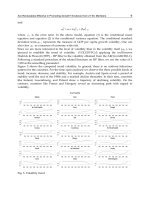
Fig. 6. Spectral radiance characteristics of Organic Light Emitting Devices (OLEDs and Si
avalanche-based light emitting device (Si Av LED), and comparison with the spectral
detection range of reach through avalanche detector (RAPD) devices.
0
10
20
30
40
50
60
70
80
90
100
0
0.001
0.002
0.003
0.004
0.005
0.006
0.007
0.008
0.009
0.01
0.011
0.012
0.013
0.014
0.015
400 500 600 700 800 900 1000 1100 1200
Quantumefficienct(%)
SpectralRadianceW(m
2
.sr.nm)
‐1
Wavelen
g
th
(
nm
)
Green et al, 2000
Kramer et al, 1993
Faucet et al, 1998
Si Av LED
Kramer, Snyman et al,
1993- 2010
OLED
Vogel et al,
2004
OLED
Vogel et al
OLED
Vogel et al
Si RAPD
20 -50 GHz
Optoelectronics – Devices and Applications
30
Si avalanche light emitting devices in the 450 – 650 nm regime have been known for a long
time (Newman 1955; Ghynoweth et al, 1956)]. The fabrication of these devices is high
temperature compatible and can be used in standard silicon designs. Viable CMOS
compatible avalanche Si LEDs (Si CMOS Av LEDs) have emerged since the early 1990’s.
Kramer & Zeits (1993) were the first to propose the utilization of Si Av LEDs inside CMOS
technology. They illustrated the potential of this technology. Snyman et al (1998-2005) have
realized a series of very practical light emitting devices in standard CMOS technology, such
as micro displays and electro-optical interfaces, which displayed higher emission efficiencies
as well as higher emission radiances (intensities). Particularly promising results have been
obtained regarding efficiency and intensity, when a combination of current density
confinement, surface layer engineering and injection of additional carriers of opposite
charge density into the avalanching junction, were implemented (Snyman et al., 2006 - 2007).
These devices showed three orders of increase in optical output as compared with previous
similar work. However, increases in efficiency seemed to be compromised by higher total
device currents; because of loss of injected carriers, which do not interact with avalanching
carriers. Du Plessis and Aharoni have made valuable contributions by reducing the
operating voltages associated with these devices (2000, 2002).
Fig. 7 presents an example of an electro-optical interface that was developed by Snyman et
al. in association with the Kramer- Seitz group in 1996 in Switzerland and which offered
very high radiance intensity (approximately 1 nW) in spot areas as small as 1 µm
2
.
The latest analysis of the work of Kramer et al and Snyman et al (Snyman et al, 2010), shows
that, particularly, the longer wavelength emissions up to 750 nm can be achieved by
focusing on the electron relaxation techniques in the purer n-side of the silicon p-n
avalanching junctions. This development has a very important implication. The spectral
radiance of this device compares extremely well with the spectral detectivity of the silicon
reach through avalanche photo detector (RAPD) technology. A particular good match is
obtained between the emission radiance spectrum of this device and the detectible spectrum
of a RAPD (see Fig. 6).
(a) (b)
Fig. 7. Si avalanche-based light emitting device (Si Av LED) and electro-optical interfaces
realized in 1.2 µm Si CMOS technology with standard CMOS design and processing
procedures (Snyman, 1996). (a) Top view with bright field optical microscopy. (b) Optical
emission characteristics in dark field conditions
1 µm
Integrating Micro-Photonic Systems into Standard Silicon CMOS Integrated Circuitry
31
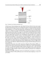
Fig. 8. Schematic diagram showing the operation principles of a Si avalanche-based light
emitting device (Si Av LED) and electro-optical interface. (a) Structure of the device. (b)
Electric field profile through the device and , (c), nature of photonic transitions in the energy
band diagram for silicon .
Fig. 8 represents some of the latest in house designs with regard to a so called “modified E-
field and defect density controlled Si Av LED“. Only a synopsis is presented here and more
details can be found in recent publications (Snyman and Bellotti, 2010a ). The device consists
of a p+-i-n-p+ structure with a very thin lowly doped layer between the p+ and the n layer.
The purpose of this layer is to create a thin but elongated electric field region in the silicon
that will ensure a number of diffusion multiplication lengths in the avalanche process. The
excited electrons loose their energies mainly in the n–type material through various intra-
band and inter-band relaxation processes. If the p
+
n junction at the end of the structure is
slightly forward biased and a large number of positive low energy holes is injected into the
n-region, these holes can then interact with these high energy electrons . This enhances the
recombination probability between high energetic electrons and low energy holes.
The recombination process can be further enhanced by inserting a large number of surface
states at the Si-SiO
2
interface in the n-region. This can cause a “momentum spread” in the n-
region for both, the energetic electrons as well as the injected holes. Fig. 8 (c) presents the
photonic transitions that are stimulated by this design. Excited energetic electrons from high
up in the conduction band may relax from the second conduction band to the first
conduction band. Energetic electrons excited by the ionization processes may interact and
relax to defect states which are situated in the mid-bandgap level between the conduction
band and the valence band. The maximum density distribution (electrons per energy levels)
is around 1 to 1.8 eV (Snyman 2010a) , and relaxation to mid-bandgap defect states will
c
Optoelectronics – Devices and Applications
32
cause a spread of light emission energies from 0.1 eV to 2.3 eV , with maximum transition
possibilities between 1.5 eV and 2.3 eV. By controlling the defect density in this device, one
can favour either the 650 nm or 750 nm emissions. Total emission intensities of up to 1 µW
per 5 µm
2
area at the Si-SiO
2
interface have recently been observed (Snyman and Bellotti,
2010a). Further improvement is currently underway in order to increase particularly the
longer wavelength emissions associated with these structures.
In summary, particularly promising about the application of Si Av LEDs into CMOS
integrated systems, is the following :
Si Av LEDs can emit an estimated 1 µW inside silicon and at compatible CMOS
operating voltages and currents (3-8 V, 0.1- 1 mA) they can emit up to 10 nW / µm
2
at
450 -750 nm (Snyman and Bellotti, 2010a; Snyman 2010b; Snyman 2010c).
They can be realized with great ease by using standard CMOS design and processing
procedures , vastly reducing the cost of such systems.
The emission levels of the Si CMOS Av LEDs are 10
+3
to 10
+4
times higher than the
detectivity of silicon p-i-n detectors, and hence offer a good dynamic range in detection
and analysis.
These types of devices can reach very high modulation speeds, greater than 10 GHz,
because of the low capacitance reverse biased structures utilised (Chatterjee, 2004).
They can be incorporated in the silicon-CMOS overlayer interface, because they are
high temperature processing compatible.
They can emit a substantial broadband in the mid infrared region (0.65 to 0.85 µm) .
Particularly, p
+
n designs emit strongly around 0.75 µm (Kramer 1993, Snyman 2010a).
4. Development of CMOS optical waveguides at 750nm
The development of efficient waveguides at submicron wavelengths in CMOS technology
faces major challenges, particularly due to alleged higher absorption and scattering effects at
submicron wavelengths.
A recent analysis shows that both, silicon nitride and Si oxi-nitride, transmitting radiation at
low loss between 650 and 850 nm (Daldossa et al., 2004; Gorin et al., 2008). Both, Si O
x
N
y
and Si
x
N
y
possess high refractive indices of 1.6 - 1.95 and 2.2 - 2.4 respectively, against a
background of available SiO
2
as cladding or background layers in CMOS silicon .
Subsequently, a survey was conducted of the optical characteristics of current CVD plasma
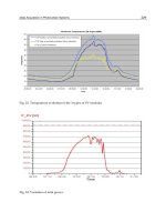
deposited silicon nitrides that can be easily integrated in CMOS circuitry. In Fig. 9, the
absorption coefficients versus wavelength are given for three types of deposited silicon
nitrides. The first curve corresponds to the normal high frequency deposition of silicon
nitride used in CMOS fabrication. The results were published by Daldossa et al. , 2004. The
second curve corresponds to a low frequency deposition process as recently developed by
Gorin et al (2008). The third curve corresponds to a special low frequency process followed
by a low temperature “defect curing” technique as developed by Gorin et al. This process
offers superb low loss characteristics. These results are extremely promising , and
calculations show that, with this technology , very low propagation losses of 0.5 dB cm
-1
at
around 750 nm can be achieved when combined with standard CMOS technology. This
wavelength falls into the maximum detectivity range of state-of-the-art reach- through
avalanche silicon photo detectors (Si-RAPDs).
Integrating Micro-Photonic Systems into Standard Silicon CMOS Integrated Circuitry
33
Fig. 9. Analyses of the loss characteristics of plasma deposited silicon nitride versus
propagation wavelength and comparison with the detectivity of CMOS compatible reach
through avalanche detectors.
Optical simulations were performed with RSOFT (BeamPROP and FULL WAVE) to design
and simulate specific CMOS based waveguide structures operating at 750 nm, using CMOS
materials and processing parameters. First, simple lateral uniform structures were investigated
with no vertical and lateral bends and with a core of refractive index ranging from n = 1.96
(oxi-nitride ) to n = 2.4 (nitride). The core was surrounded by silicon oxide (n = 1.46).
The analysis showed that both, multimode as well as single mode waveguiding can be
achieved in CMOS structures. Fig. 10 and Fig.11 illustrate some of the obtained results.
Fig. 10 shows a three dimensional view of the electrical field along the 0.6 µm diameter
silicon nitride waveguide. Multi-mode propagation with almost zero loss is demonstrated as
a function of distance over a length of 20 µm. Multi-mode propagation in CMOS micro-
systems has the following advantages: (1) a large acceptance angle for coupling optical
radiation into the waveguide; (2) exit of light at large solid angles at the end of the
waveguide; (3) allowing narrow curvatures in the waveguides; and (4) more play in
dimensioning of the waveguides. (1) and (2) are particularly favourable for coupling LED
light into waveguides.
Fig. 11 shows the simulation of a 1 µm diameter trench-based waveguide with an embedded
core layer of 0.2 µm radius silicon nitride in a SiO
2
surrounding matrix. The two
dimensional plot of the electrical field propagation along the waveguide as shown in Fig. 11
(a) reveals single mode propagation. The calculated loss curve in the adjacent figure (b),
shows almost zero loss over a distance of 20 µm in Fig 11(b). Fig. 12(a) displays the
transverse field in the waveguide perpendicular to the axis of propagation. Using the value
of the real part of the propagation constant, as derived in the simulation, an accurate energy
loss could be calculated using conventional optical propagation. With the imaginary part of
the refractive index, as predicted by RSOFT, a low loss propagation of 0.65 dB cm
-1
is found,
taking the material properties into account, as used by the RSOFT simulation program.
Optoelectronics – Devices and Applications
34
Fig. 10. Advanced optical simulation of the electrical field propagation in a 0.6 µm wide
silicon nitride layer embedded in SiO
2
in CMOS integrated circuitry. Multimode optical
propagation at 750 nm is demonstrated over 20 µm with a loss of less than 1 dB cm
-1.
Single mode propagation, where the light is more difficult to couple into the waveguide,
results in low modal dispersion loss along the waveguide, as well as in extreme high
modulation bandwidths.
It is important to note that waveguide mode converters can be designed to convert
multimode into single mode.
In Fig 12 (b) , the same simulation was performed as in Fig. 11, but with a silicon oxi-nitride
core of 0.2 µm embedded in a silicon oxide cladding. The mode field plot shows a slight
increase in the fundamental mode field diameter, and less loss of about 0.35 dB cm
-1
. This
suggests that a larger proportion of the optical radiation is propagating in the silicon oxide
cladding.
(a) (b)
Fig. 11. (a) and (b): Advanced simulation of the electrical field propagation in a silicon nitride
layer within CMOS integrated circuitry. Single mode propagation is demonstrated at 750 nm
over a distance of 20 µm for a 0.2 µm wide silicon nitride waveguide , embedded in SiO
2
.
Integrating Micro-Photonic Systems into Standard Silicon CMOS Integrated Circuitry
35
(a) (b)
Fig. 12. (a) Transverse field profile prediction for a silicon nitride based CMOS waveguide.
The core of the silicon nitride is 0.2 µm in diameter and is embedded in a 1 µm diameter
SiO
2
cladding. (b) Transverse mode field profile for a 0.3 µm oxi-nitride layer embedded in
SiO
2
.
Subsequently, a modal dispersion analysis was conducted on these structures. The
calculations reveal a maximum dispersion of 0.5 ps cm
-1
and a bandwidth-length product of
greater than 100 GHz-cm for a 0.2 µm silicon nitride based core. A maximum modal
dispersion of 0.2 ps cm
-1
and a bandwidth-length product of greater than 200 GHz-cm was
found for a 0.2 µm silicon-oxi-nitride core which was embedded in a 1 µm diameter silicon-
oxide cladding. Due to the lower refractive index difference between the core and the
cladding, a larger transverse electric field of about 0.5 µm radius, as well as lower modal
dispersion, is achieved with a silicon oxi-nitride core. The material dispersion characteristic
was estimated at approximately 10
-3
ps nm
-1
cm
-1
, which is much lower than the maximum
predicted modal dispersion for the designed waveguides.
5. CMOS optical link - proof of concept
The photo-micrographs in Fig. 13 illustrate results which have been achieved with a CMOS
opto-coupler arrangement, containing a CMOS Av-based light-emitting source, an 5 x 1 x
150 µm silicon over-layer waveguide and a lateral incident optimized CMOS based photo-
detector (Snyman &Canning 2002, Snyman et al, 2004). The waveguide was fabricated in
CMOS similar to that as shown in Fig. 5 (b).
Fig. 13 (a) shows an optical microscope picture of the structure under normal illumination
conditions with the Si LED source, the waveguide and the elongated diode detector. Fig.13
(b) shows the structure as it appeared under subdued lighting conditions. At the end of the
silicon oxide structure, some leakage of the transmitted light was observed (feature B). This
observation is quite similar to light emission observed at the end of a standard optical fibre,
and it confirms that good light transmission occurs along the waveguide.
Optoelectronics – Devices and Applications
36
(a)
(b)
Fig. 13. Photomicrographs of a CMOS opto-coupler arrangement consisting of a CMOS Av-
based light-emitting source, an optically waveguide and a CMOS lateral incident photo-
detector. (a) shows a bright field photo-micrograph of the arrangement, and (b) shows the
optical performance as observed under dark field conditions (Snyman et al, 2000, 2004).
Signals of 60 – 100 nA could be observed for 0 to +20 V source pulses and +10 V bias at the
elongated diode detector. When the detector was replaced with a n
+
pn photo-transistor
detector (providing some internal gain at the detector at appropriate voltage biasing),
signals of up to 1 µA could be detected.
The arrangement showed good electrical isolation of larger than 100 MΩ between the Si
LED and the detector for voltage variations between the source and the detector of 0 to +10V
on either side when no optical coupling structures were present . This was mainly due to the
p
+
n and n
+
p reversed biased opposing structures utilised in the silicon design. Once an
avalanching light emitting mode was achieved at the source side, a clear corresponding
current response was observed at the detector. Detailed test structures are currently
investigated.
6. Proposed CMOS and SOI waveguide-based optical link technology
Building on the optical source and waveguide concepts, as outlined in the preceding
sections, optical source based systems may be designed which optimally couple light into
the core of an adjacently positioned optical waveguide. Similarly, the core of the waveguide
can laterally couple light into an adjacent RAPD based photo diode. It follows that
Si LED
Waveguide Detector
50
m
B
Integrating Micro-Photonic Systems into Standard Silicon CMOS Integrated Circuitry
37
interesting high speed source- detector optical communication channels and systems can be
implanted in CMOS technology as illustrated in Fig. 14 (Snyman , 2010d, 2011a). The
proposed isolation trench waveguide technology as outlined in Section. 2 is particularly well
suited in order to create such configurations in CMOS technology. However, OLED surface
layer structures together with CMOS technology and Si Av LED and SOI technologies may
also generate such structures.
Fig. 14. Conceptual optical link design using a optical source arrngement as in Fig . 8 , a
CMOS trench based waveguide and a RAPD photo detector arrangement.Bi-directional
optical communication may be realised with the structure.
Using a Si Av LED optical source, an optical p
+
npn source, as outlined in Fig. 8 can be
designed, with its optical emission point aligned with a lateral propagating CMOS based
waveguide. Similarly, lateral incident detectors can be designed that take advantage of the
carrier multiplication and high drift concept of reach through avalanche based diodes
(RAPD). This can be combined with the proposed CMOS trench- waveguide systems. This
implies that a similar lateral n+pp-p+ structure could be designed, such that with suitable
voltage biasing, a high carrier generation adjacent to a high carrier drift region is formed. By
placing an appropriate contact probe in the high drift region, varying voltage signals could
be detected as a function of drift current. Silicon detector technology has been quite well
established during the last few decades. These devices enerate up to 0.6 A W
-1
and reach up
to 20 GHz (Senior, 2008).
The generic nature of these designs open up numerous and diverse types of optical
communication and optical signal processing devices realized in CMOS technology.
Transmitter-receiver arrangements can be designed that will enable full bi-directional
optical communication. The concepts, outlined here are not final , and there is scope for
further improvement.
A drawback of these designs is the fact that the optical source needs to be driven by direct
modulation methods. OLEDs have the advantage of low modulation current or voltage.
However, they may be limited by forward biased diffusion capacitance effects. Si Av LEDs
require low modulation voltage, but high driving currents. Since the driving current needs
CMOS
OXI‐TRENCH
WAVEGUIDE
SIGNAL
DETECTION
BIAS
CMOS
MOD‐E
SiAVLED
CMOS
MOD‐E
SiDETECTOR
BIAS
MODULATION
Optoelectronics – Devices and Applications
38
to be supplied by CMOS driver circuitry, this implies large area CMOS driving PMOS and
NMOS transistors with high capacitance. Through the incorporation of localized hybrid
technologies, appropriate waveguide based modulators can be designed , that are either
based on the electro-optic ( Kerr) effect or the charge injection effect It is envisaged to reach
modulation speeds, orders of magnitude higher (reaching far into the GHz range), with
much less driving currents (Snyman, 2010d).
7. Optical coupling efficiencies and optical link power budgets
Obtaining good coupling efficiencies with Si Av LEDs and OLEDs when incorporated into
CMOS structures presents a major challenge. It is estimated that the optical power emitted
from the Si Av LEDs is in the order of 100 – 1000 nW (for typical driving powers of 8 V and
10 µA). Since most of the emission occurs inside the silicon with a refractive index of 3.5, it
implies that only about 1 % of this optical power can leave the silicon because of the small
critical angle of only 17 degrees inside the silicon. After leaving the silicon the light spreads
over an angle of 180 degrees (Fig.15 (a)). When a standard multimode optical fibre with a
numerical aperture of 0.3 is placed close to such an emission point, only 0.3 % of the forward
emitted optical power enters the fibre.
Our research has shown that remarkable increases in optical coupling efficiencies can be
achieved by means of two techniques : (1) concentrating the current that generates the light
as close as possible to the surface of the silicon ( for Si Av LEDs) ; and, (2), maximizing the
solid angle of emission in the secondary waveguide.
By displacing the metal contacts that provide current to the structure as shown in Fig 15 (b) ,
the current is enforced on the one side surface facing the core of the waveguide. Since
mainly surface emission is generated, about 50 % of the generated optical power enters the
waveguide (Snyman 2010d, Snyman 2011 a). A silicon nitride core with a silicon oxide
cladding could then ensure an acceptance angle of up to 52.2 degrees within the waveguide.
The total coupling efficiency that can be achieved with such an arrangement is of the order
of 30%. This is an 100 fold increase in coupling efficiency from the point of generation to
within the waveguide as achieved in Fig 15 (a) (Snyman, 2011c).
(a) (b) (c)
Fig. 15. Demonstration of optical coupling between a Si Av LED optical source and the
silcon nitride CMOS based optical waveguide.
Integrating Micro-Photonic Systems into Standard Silicon CMOS Integrated Circuitry
39
Fig. 15 ( c) shows a further optimized design. Here a thin protrusion of doped silicon
material is placed inside the core of a silicon nitrate core CMOS based waveguide (Snyman
2011a). Such a design is quite feasible with standard layout techniques of
CMOS silicon provided that the side trenches surrounding the silicon protrusion are
effectively filled with silicon nitride through the plasma deposition process. The core is
surrounded by trenches of silicon oxide. The optical power that is generated at the tip of the
protrusion and radiates in a solid angle of close to a full sphere inside the waveguide.
Simulation studies show that up to 80 % of the emitted light is now coupled into the silicon
nitride core. Reflective metal surfaces at the sides and the back of this waveguide may
further improve the forward propagation.
The optical radiation produced inside these waveguides will be highly multimode. The
diameters of these waveguides may be bigger than the ones suggested for single mode
propagation in Section 4. However, in such cases, standard type waveguide mode
converters can reduce the number of modes or even generate single mode propagation.
With an optical power source of 1 µW at the silicon surface, one can achieve a coupling
efficiency between source and waveguide of 30 to 50 %, assuming a coupling loss of only 3
dB between source and waveguide. With a 0.6 dB cm
-1
wave guide loss, the loss in the 100
µm waveguide itself is estimated to be 0. 01 dB. Since the whole radiation propagating in the
waveguide can be delivered with almost 100 % coupling efficiency, one can expect about 500
nW of optical power reaching the detector. With an 0.3 A per Watt conversion efficiency of
the detector, current levels of about 100 nA (0.1 µA) can be sensed with a 10 x 10 µm
detector. Values for OLEDs together with surface CMOS waveguides could be much higher.
The low frequency detection limit of silicon detectors of such dimensions is of the order of
pico-Watt. For low frequencies and low optical level detection , a dynamic range of about
10
3
to 10
4
is achievable. At high modulation speeds, the achievable bit error rates will
obviously increase.
The optical powers quoted above are much lower when compared with current LASER,
LED and optical fiber link “macro” technology. However, we are addressing a new field of
“micro-photonics” with micrometer and nano-meter dimensions, and power levels as well
as other parameters should be scaled down accordingly. Furthermore, our research showed
that the optical intensities determine the achievable bit error rates rather than absolute
intensities. As stated earlier, the calculated intensity levels with some of our Si Av LEDs are
as high as 1 nW µm
-2
.
8. Connecting with the environment
We present only two viable ways of communicating with the outside chip environment:, i.e
optical communication vertically outward from the chip, and optical communication via
lateral waveguide connections.
In the first case, silicon oxide and silicon nitride are used as well as trench technology as
outlined in Section 2 in order to increase the vertical outward radial emission (Snyman,
2011c). Fig. 16 illustrates the concept. By placing a thin layer of silicon adjacent to two semi-
circular trenches, the solid angle of the optical outward emission is increased within the
silicon from about 17 to almost 60 degrees. Filling up the trenches with silicon oxide and
placing of thin layer of silicon oxide increases the critical emission angle from the silicon
from 17 to 37 degrees. The thin layer of silicon nitride can be appropriately shaped with post
processing RF etching techniques such that all emitted light can be directed vertically
Optoelectronics – Devices and Applications
40
upward. It is estimated that a total optical coupling efficiency from silicon to fibre of up to
40 % can be achieved in this way.
Fig. 16. Vertical outward coupling of optical radiation into optical fiber waveguides using
trench based and overlayer post processing technology.
Fig. 17. Lateral out coupling using CMOS waveguide based optical coupling with optical
fibers alligned at the side surface of the chip.
Die side
surface
Waveguide
core
Si Av LED
Si Av LED
Si Nitride
or polymer
lens
CMOS Top
Surface
Si Oxide
Layer
Integrating Micro-Photonic Systems into Standard Silicon CMOS Integrated Circuitry
41
In the second case, optical coupling is achieved via lateral wave guiding (Snyman, 2010 d,
2011 c, 2011d). Fig. 17 illustrates this. (1) The lateral coupling from the optical source can be
as high as 80 % as demonstrated in the previous section in Fig. 15 (c ). (2) The optical
radiation can be converted from multi-mode propagation to single mode propagation by
waveguide mode converters; (3) Single mode radiation at the side surface ensures high
collimation. This assures a coupling efficiency of almost 100 % at the side surface. In total, an
optical coupling efficiency of up to 80 % can be achieved. This is much higher than
achievable with vertical coupling. (4) Our analysis shows that the far field pattern of the
optical radiation emitted from the waveguides can be manipulated by either adiabatic
expansion or by tapering the core near the end of the waveguide. In this way the mode field
diameter extends into the silicon oxide cladding, and the radiation couples more efficiently
into the core from an externally positioned optical fibre.
In conclusion, the analysis shows that combining CMOS compatible sources effectively with
on- chip lateral extending waveguide technology, offers major advantages , like increased
coupling efficiencies, increased optical power link budgets, lower achievable bit error rates
in data communication , and better coupling with the external environment.
9. Proposed first iteration CMOS micro-photonic systems
The on-chip optical and signal processing applications have been already highlighted in
Section 6. A particular interesting design , made possible with the CMOS waveguide
technology, is a so called H-configuration waveguide that can be used for optical clocks in
very large CMOS micro-processor systems (Wada, 2004).
The realization of diverse other CMOS and waveguide based micro-photonic systems as
well as the incorporation of a whole range of micro-sensors into CMOS technology is
possible. The advantages are, (1), high levels of miniaturization; (2), higher reliability levels;
(3), a vast reduction in technology complexity and, (4), a drastic reduction in production
costs. The proposed waveguide technologies, particularly in this chapter, offer high optical
coupling between Si Av LEDs or OLEDS and CMOS based waveguides, with diverse
applications in optical interconnect and future on chip micro-photonic systems.
Fig. 18 to 20 illustrate some applications, as proposed here, for CMOS based micro-photonic
systems (Snyman 2008a, 2009a, 2010c, 2011b, 2011c).
In Fig. 18, a hybrid approach is demonstrated. A mechanical module is added to an existing
CMOS package creating a CMOS-based micro-mechanical optical sensor (CMOS MOEMS),
capable of detecting diverse physical parameters such as vibration , pressure, mechanical
osscillation etc. Optical radiation is coupled from the CMOS platform to the mechanical
platform. The mechanical platform returns optical signals which contain information about
the deflection (Snyman, 2011 c).
Fig. 19 shows a monolithic approach of creating CMOS MOEMS involving only post-
processing procedures. A cantilever is fabricated in part of the CMOS IC die, by post
processing procedures. Si Av LED or OLEDs couple optical radiation into a slanted
waveguide track, transmit the optical radiation laterally across the die, collimate the
radiation through the crevasse onto the one side of the cantilever. Optical radiation is
reflected from the cantilever and detected by a series of p-i-n photo- detectors arranged
laterally along the crevasse side surface. The accumulated signals are processed by adjacent
Optoelectronics – Devices and Applications
42
CMOS analogue and digital processing circuits. Such a structure can detect vibrations,
rotations and accelerations (Snyman, 2011 c).
Fig. 18. Schematic diagram of a hybrid CMOS-based micro-photonic system that can be
realized by placing a mechanical- module on top of a optically radiative and detector active
CMOS platform using standard packaging technology.
Fig. 19. Schematic diagram of an example CMOS-based Micro-Mechanical-Optical Sensor
(MOEMS) device that can be realized with conventional CMOS integrated design with
additional post processing procedures. Key constituents of such a device is an effective
CMOS on-chip optical source , coupling of the source to a waveguide, CMOS competible
optical waveguiding and optical collimation and detection circuitry.
CMOS adjacent
circuit ry
CMOS SiAv LED
CMOS waveguide
Cantilever
structure
Detector
elements
CMOS Amplification
circuitry
Integrating Micro-Photonic Systems into Standard Silicon CMOS Integrated Circuitry
43
The immunity to electromagnetic induced noise of these systems is a major advantage. Key
components of such the systems are an effective CMOS compatible optical source, CMOS
compatible optical wave guiding, effective optical coupling into the waveguide, and optical
collimation circuitry. The sensitivity and functionality of these systems are a function of the
waveguide design.
Fig. 20 explores a more complete and more advanced waveguide based micro-photonic
system design including ring resonators, filters and an unbalanced Mach-Zehnder
interferometer. By selectively opening up a portion of the waveguide in the one arm of the
interferometer to the environment, molecules or gases can be absorbed and both, phase and
intensity changes can be detected by the interferometer. Sensors can be designed which
detect the absorption spectra of liquids (Snyman 2008a, 2009a, 2010c, 2011b, 2011c,).
Fig. 20. Schematic diagram of a CMOS-based micro-photonic system that can be realized
using an on chip Si Av LED, a series of waveguides, ring resonators and an unbalanced
Mach-Zehnder interferometer. A section of the waveguide is exposed to the environment
and can detect phase and intensity contrast due to absorption of molecules and gases in the
evanescent field of the waveguide.
OPTICAL
DETECTOR
CMOS LED
COUPLER
RING
RESONATOR
GAS AND LIQUID
INTERACTION
AREA
W
A
VEGUIDE
INTERACTION
AREA
UNBALANCED
MACH ZENDER
PHASE
INTERFEROMETER
DROP λ
Optoelectronics – Devices and Applications
44
Obviously, a great variety of diverse other types of CMOS based micro-photonic systems are
possible, each incorporating specific optical micro-sensors and waveguides. It is anticipated
to implement future CMOS based micro-photonic systems in micro-spectro-photometry,
micro-metrology, and micro- chemical absorption analysis.
10. Conclusions
It is evident that the analyses as presented in this study with regard to Si Light Emitting
Devices operating at 650 – 850 nm and lateral optical waveguides can lead to the generation
of diverse photonic micro-systems systems in standard CMOS integrated circuitry. The
generation of lateral waveguides in CMOS technology operating in this wavelength regime
poses particular challenges. However, enough evidence has been obtained from our
analyses and first iteration experimental realisations that this technology is indeed feasible.
The proposed sub-technologies has major advantageous for the generation of complete new
families of photonic micro-systems on CMOS chip avoiding the more complex Si Ge or III-V
hybrid technology. The following serves as brief summaries of results and statements made:
1. The potential of CMOS technology was analysed and evaluated for sustaining the
generation of optical micro-photonic systems in CMOS integrated circuitry.
Particularly, the silicon dioxide “field “ oxide , inter-metallic oxides and passivation
nitride and added polymer over-layer structures show good potential to be utilised as
“building blocks” in new generation CMOS based micro-photonic systems.
2. It was shown that a variety of optical source technologies currently already exists that
can be utilised for the generation of 650- 850nm optical sources on chip. OLEDs offers
high irradiance in this wavelength regime. There are however challenges with regard to
incorporation of the hybrid organic based technologies into CMOS technology and with
regard to achieving high modulation speeds. Silicon avalanche-based Si LEDs can be
integrated into CMOS integrated circuitry with relative ease, they offer high
modulation bandwidth , and can be integrated particularly at the silicon-overlayer
interface, and offer both vertical and lateral optical coupling possibilities. Their power
conversion efficiency is lower, but analysis show that the power levels is enough to
offer adequate power link budgets , with high modulation bandwidth. Particularly,
they can generated micron size optical emission points, with high irradiance levels,
offering unique application possibilities with regard to generating of micro-structured
photonic devices.
3. Analyses and simulation results as presented in this study, show that it is possible to
design waveguides with CMOS technology at 650-850 nm. Particularly, the generation
of waveguides with small dimension silicon nitride cores embedded in larger silicon
dioxide surrounds seems particularly attractive. The utilisation of lateral CMOS
waveguides increase coupling efficiencies, improve optical link power budgets, and
supports numerous designs with regard to the generation of micro-photonic structures
in CMOS integrated circuitry. These aspects are all beneficial for generating lateral
layouts of micro-photonic systems on chip and offers viable options for interfacing
optically with the environment
4. The technology as proposed, may not necessarily compete with the ultra high
modulation speeds offered by Si-Ge based and SOI based technologies currently
Integrating Micro-Photonic Systems into Standard Silicon CMOS Integrated Circuitry
45
operating at above 1100nm. However, Si Av LEDs, waveguides detectors, demonstrated
in this study, support the generation of micro-photonic systems in standard CMOS
technology, offering modulation speeds of up to 10 GHz at the added advantage of ease
of integration into standard integrated circuit technology. Direct driving of the sources
in CMOS may reduce modulation speeds. Particularly, the use of waveguide-based
modulators may produce higher modulation speeds (Snyman 2010e). Several advances
in this area could still be made.
5. Lastly, a few designs are proposed for the realisation of first iteration micro-photonic
sensor systems on chip. Both mechanically as well as adhesion and waveguide based
sensors systems are proposed and the application possibilities of each were
presented. Particularly, the proposed technologies offers the realisation of a complete
new family of source–sensor based micro-photonic systems where bandwidth is not
the essential parameter, but rather the capability to add to the integration level,
intelligence level, and the interfacing level of the processing circuitry with the
environment.
11. Acknowledgements
The hypotheses, analyses, first iteration results and research interpretations as presented in
this study were generated by means of South African National Research Foundation grants
FA200604110043 (2007-2009) and NRF KISC grant 69798 (2009-2011) and SANRF travel
block grants (2007,2008, 2009). The utilization of facilities at the Carl and Emily Fuchs
Institute for Microelectronics for confirmation of some of the experimental results is
gratefully acknowledged. The provision and use of advanced software facilities at the TUT
is acknowledged. The final proof reading of the script by Dr. D. Schmieder is especially
acknowledged.
Selected topics of this article forms the subject of recent PCT Patent Application
PCT/ZA2010/00032 of 2010, (Priority patents: ZA2010/00200, ZA2009/09015,
ZA2009/08833, ZA2009/04508) ; PCT Patent Application PCT/ZA2010/00033 of 2010
(Priority patents: ZA 2008/1089, ZA2009/04509, ZA2009/04665, ZA2009/04666,
ZA2009/05249, ZA2009/08834, ZA2009/0915), ZA2010/08579, ZA2011/03826; and PCT
Patent Application PCT/ZA2010/00031 of 2010” (Priority patents: ZA 2010/02021, ZA
2010/00201, ZA2010/00200, ZA 2009/07233, ZA2009/07418, ZA 2009/04164,
ZA200904163, ZA2009/04161). These all deal with our latest technology definitions with
regard to OLED and Si Av LED CMOS based optical communication systems, Si Av LED
design, CMOS waveguide design, CMOS modulator and switch design, CMOS based data
transfer systems, CMOS micro-photonic system and Micro-Optical Mechanical Sensors
(MOEMS) design. The purpose of these patents is to secure intellectual property
protection on investments made already, and to secure licensing of certain key
components of the technology as already developed. However, the opportunities in this
field is so extensive, that numerous further investment opportunities with interested
further investors exist.
12. References
Aharoni, H. & Du Plessis, M., "The Spatial Distribution of Light from Silicon LED's", Sensors
and Actuators, Vol. A 57 No. 3, (1996), pp. 233-237.
Optoelectronics – Devices and Applications
46
Beals, M., Micheal, J., Liu, F.J, Ahn, D.H, Sparacin, D. , Sun, R., Hong, C.Y. & Kimerling,
L.C., (2008) , “Process flow innovations for photonic device integration in CMOS”,
Proceedings of SPIE 6898, pp. 6898 O4 – O14.
Bourouina, T. , Bosseboeuf, A. & Grandchamp, J-P, (1996) . "Design and Simulation of an
Electrostatic Micro-pump for Drug-Delivery Applications". MicroMechanics Europe
Workshop (MME'96), pp 152-155, Barcelone .
Brummer, J. C., Aharoni, H. ,& du Plessis, M. , "Visible Light from Guardring Avalanche
Silicon Photodiodes at Different Current Levels", South African Journal of Physics
Vol. 16 (1/2),(1993), pp 149-152.
Bude, J., Sano, & N., Yoshii, A. , “Hot carrier Luminescence in Silicon”, Physical Review Vol.
B 45, No. 11, (1992), pp. 5848 – 5856.
Carbone, L. , Brunetti, R., Jacoboni, C. , Lacaita, A. & Fischetti, M. , “Polarization analysis of
hot-carrier emission in silicon, “ Semicond.Sci. Technol. Vol. 9, (1994), pp. 647-
676.
Chatterjee, B., Bhuva & Schrimpf, R., “High-speed light modulation in avalanche
breakdown mode for Si diodes”, IEEE Electron Device Letters , Vol. 25, No. 9,(2004),
pp. 628-630.
Claeys, C., (Fellow, IEEE), (2009). “Trends and Challenges in More Moore and More than
Moore Research”, Proceedings of the South African Conference on Semiconductors and
Superconductors ( SACSST), pp 1-6 , ISBN 978-0-620-43865-0, Cape Town, South
Africa.
Daldosso,N., Melchiorri, M., Riboli, F., Sbrana, F., Pavesi, L., Pucker,G., Kompocholis, C.,
Crivellari,M., Belluti, P., & Lui, A., “Fabrication and optical characterization of thin
two-dimensional Si
3N4 waveguides” Mater. Sci. Semicond. Process. Vol. 7, (2004), pp.
453-458.
Du Plessis, M ., Aharoni, H. & Snyman, L.W., “A silicon trans-conductance light emitting
device (TRANSLED).” , Sensors and Actuators , Vol. A 80, No. 3, (2003), pp 242-
248.
Du Plessis, M., Aharoni, H. , & Snyman, L.W., “ Spatial and intensity modulation of light
emission from a silicon LED matrix”, IEEE Photonics Technology Letters , Vol. 14, No.
6, (2002), pp. 768-770.
Du Plessis, M., Snyman, L.W. , & Aharoni, H. (2003). “ Low-Voltage Light Emitting Devices
in Silicon IC Technology”, Proc. of the IEEE International Symposium on Industrial
Electronics (ISIE 2005), Vol. 3 , ISBN 0-7803-8739-2 , pp. 1145- 1149, Dubrovnik,
Croatia.
Fauchet, P. M., "Progress Toward Nano-scale Silicon Light Emitters", IEEE Jour. Selected
Topics in Quantum Electron Vol.4, (1998) , pp. 1020-1028.
Fitzgerald, E.A. ,& Kimerling, L.C. , “Silicon-Based Technology for Integrated Opto-
electronics”, MRS Bulletin, (1998), pp. 39-47.
Foty, D., “Digital CMOS Electronics“, Gilgamesh Associates, LLC, Fletcher, Vermont, USA.
(2009). Private communication .
Fullin, E., Voirin,E., Lagos, A., Moret, J.M., “MOS-Based Technology for Integrated Opto-
electronic Circuits”, Scientific and technical report, CSEM, (1993), pp. 26.
Integrating Micro-Photonic Systems into Standard Silicon CMOS Integrated Circuitry
47
Ghynoweth, W.G. & McKay, K.G. , “Photon emission from avalanche breakdown in silicon
“, Physical Rev. Vol. 102 , (1956), pp. 369-376.
Gianchandani , Y. B. , (Fellow, IEEE), (2010) “ Emerging Research in Micro and Nano
Systems: Opportunities and Challenges for Societal Impact” , In: Microfluidics,
BioMEMS, and Medical Microsystems VIII, edited by Holger Becker and Wanjun
Wang, Proc. of SPIE, available at doi: 10.1117/12.848216 (Plenery lecture).
Gorin, A., Jaouad, A., Grondin, E., Aimez, V. & Charette, P. , “ Fabrication of silicon nitride
waveguides for visible-light using PECVD: a study of the effect of plasma
frequency on optical properties”. Optics Express,Vol. l16, No. 18, (2008), pp 13509-
13516.
Green, M.A., Zhao, J., Wang, A. , Reece, P. & Gal , M., “Efficient silicon light-emitting
diodes” Nature , Vol. 412, (2001), pp 805-808.
Gunn ,G., Narasimha, A., Analui, B. , Liang, Y. & Sleboda, T.J. (2007) “A 40Gbps CMOS
Photonics Transceiver”,. In: Silicon Photonics II , Proc SPIE , Vol. 6477, (ISBN
9780819465900), pp. 64770N1- 8.
Hirschman, K. D., Tsybeskov, L., Duttagupta, S. P. & Fauchet, P. M. , ‘‘Silicon-based visible
light-emitting devices integrated into microelectronic circuits,’’ Nature, Vol. 384,
(1996), pp. 338–341.
Kramer, J. , Seitz, P. , Steigmeier, E. F. , Auderset, H., and Delley, B., “Industrial CMOS
technology for the integration of optical metrology systems,’’ Sensors and Actuators
A Vol. A37–38,(1993), pp. 527–533.
Kubby, J. A . & Reed, G. (2007). Introductory remarks, In: Silicon Photonics II , Proc. SPIE,
Vol. 6477. (ISBN 9780819465900), pp. xi.
Kubby, J. A.& Reed, G. (2010). Introductory remarks. In: Silicon Photonics V , Proc SPIE Vol.
6477, ISBN 9780819480026, pp xi.
Lacaita, K., Zappa, F, Bigliasrdi, S. & Manfredi, M. , “On the Brehmstrahlung origin of hot-
carrier-induced photons in silicon devices”, IEEE Trans. Electron Devices, Vol. ED40,
(1993), pp. 577-582.
Liu, J., Sun, X. , Rodolfo Camacho-Aguilera, R., Kimerling, L.C. and Michel, J. , “ Ge-on-Si
Laser operating at room temperature” Optics Letters Vol. 35, No. 5, (2010), pp. 679-
681.
Newman, R. , “Visible light emission from a silicon p-n junction”, Phys. Rev. Vol. 100, (1955),
pp. 700 – 703.
Ogudo, K. A. , Snyman , L.W. , Du Plessis, M. & Udahemuka, G. (2009). “Simulation of Si
LED (450nm-750nm) light propagation phenomena in CMOS integrated circuitry
for MOEMS applications” , Proceedings of the South Africa Conference on
Semiconductor and Superconducting Technologies ( SACSST 2009 ), ISBN 978-0-620-
43865-0, pp. 168-182.
Robbins, D.J. , Editorial comments . (2000). “Silicon Opto-electronics” , Proc. of SPIE, Vol.
3953, pp. vi, San Jose, California, USA.
Savage, N., "Linking with Light", IEEE Spectrum, Vol. 39, (2002), pp. 32–36.
Schneider, K., and Zimmerman, H. , In: Highly sensitive optical receivers , (2006) , Springer,
ISBN 13978-3-546-29613-3.
Optoelectronics – Devices and Applications
48
Sedra , A.S. & Smith, K.C. (2004 ). “VLSI Fabrication Technology” In:Microelectronics
Circuits, Oxford University Press, New York, ISBN 13:978-0-19-514252-5, pp. A
12.
Senior, J. M. , “Optical Detectors”, In: Optical Fiber Communications, Principles and Practice,
(3rd Edition), (2008). Prentice Hall. pp 444
Snyman , L. W. , Ogudo , K.A. , Du Plessis M. & Udahemuka , G. , (2009). “Application of Si
LED’s (450nm-750nm) in CMOS integrated circuitry based MOEMS - Simulation
and Analyses”, Proc. SPIE, Vol. 7208, pp. 72080C (ISSN 0277-786X ) Available at
Snyman L. W. “Hybrid and monolithic Microsystems and MOEMS”, (2011). RSA Patent
application 2011/03826 of 25
th
May 2011.
Snyman L. W., “CMOS LED MOEMS Devices”, (2008), RSA Patent Appl. No. 2008/1089, of
1 February 2008 .
Snyman, L . W. , Du Plessis, M.,& Aharoni, H . , (2005). “Three terminal optical sources
(450nm - 750nm) for next-generation silicon CMOS OEIC’s” , 12th International
Conference of Mixed Design of Integrated Circuits and Systems (MIXDES’2005), pp. 737
– 747. Krakov, Poland (Invited plenary session paper).
Snyman, L. W. , & Du Plessis, M. (2008). “Increasing The emission intensity of p
+
np
+
CMOS
LED’s (450 – 750 nm) by means of depletion layer profiling and reach-through
techniques” ; In: Silicon Photonics III , Edited by Joel A Kubby and Graham T. Reed,
Proc. SPIE , Vol. 6898 , pp. OE 1- 12, ISSN: 0277-786X, ISBN 9780819470737SPIE,
Bellingham, W.A.
Snyman, L. W. , Aharoni, H. and Du Plessis, M, “Two order increase in the quantum
efficiency of silicon CMOS n
+
pn avalanche-based light emitting devices as a
function of current density” IEEE Photonic Technology Letters, Vol. 17, (2005), pp.
2041-2043.
Snyman, L. W. , du Plessis, M. & Aharoni, H. (2006). “Two order increase in the optical
emission intensity of CMOS integrated circuit LED’s (450 – 750 nm). Comparison of
n
+
pn and p
+
np designs ”, Proc of the SPIE , Vol. 5730, pp. 59-72.
Snyman, L. W. , Du Plessis, M. & Aharoni, H. , “Injection-avalanche based n+pn Si CMOS
LED’s (450nm . 750nm) with two order increase in light emission intensity -
Applications for next generation silicon-based optoelectronics”, Jpn. J. Appl. Physics
Vol. 46 No. 4B, (2007), pp. 2474-2480.
Snyman, L. W. “CMOS waveguide based transceiver “, (2010). RSA Patent Application 2010
/06804 of 23 September 2010.
Snyman, L. W. “OLED and CMOS based micro-photonic systems“, (2010). RSA Patent
Application 2010 /08579 of 30 November 2010.
Snyman, L. W., du Plessis, M., & Bellotti, E. , “Increasing the emission intensity of p
+
np
+
CMOS LED’s (450 – 750 nm) by means of depletion layer profiling and defect
engineering techniques”, IEEE Journal of Quantum Electronics , Vol. 46 , No. 6,
(2010), pp. 906-919.
Snyman, L. W., Ogudo, K. D. and Foty, D. (2011). “Development of a 0.75 micron
wavelength CMOS optical communication system “, Proc SPIE Vol 7943, edited by
Integrating Micro-Photonic Systems into Standard Silicon CMOS Integrated Circuitry
49
Joel A. Kubby, Graham T. Reed, CCC code: 0277-786X/11/$18 doi: 10.1117/
12.873202, pp 79430K-1 to 12.
Snyman, L. W., T. Okhai, T. Bourouina
and W. Noell, (2011) “Development of on-CMOS
chip Micro-Photonic and MOEMS Systems “ Proc SPIE Vol 7930. MOEMS and
Miniaturized Systems X, edited by Harald Schenk, Wibool Piyawattanametha, CCC
code: 0277-786X/11/$18 · doi: 10.1117/12.873353, pp 79300Z-1 to 11.
Snyman, L.W. (2010d)., “Optical communication system”. PCT Patent Application
PCT/ZA2010/00032.
Snyman, L.W. , Aharoni, H ., du Plessis, M. , & Gouws, R.B.J. , “Increased efficiency of
silicon light emitting diodes in a standard 1.2 micron complementary metal oxide
semiconductor technology”, Optical Engineering , Vol. 37, (1998), pp. 2133 –
2141.
Snyman, L.W. , Aharoni, H., du Plessis, M. , Marais, J.F.K , van Niekerk, D. & Biber, A.,
”Planar light emitting electro-optical interfaces in standard silicon complementary
metal oxide semiconductor integrated circuitry", Optical Engineering , Vol. 41,
(2002), pp 3230 – 3240.
Snyman, L.W. , Auderset, H., Derendinger, M. , Patterson, B.D. , & Von Lanthen, A. ,
“Efficient electroluminescence from 2- and 3-junction silicon structures”, In: Annual
Report 1996/Annex.111B of the Paul Scherrer Institute, Switzerland, Vol. 28 ,
(1996).
Snyman, L.W. , Bogalecki, A. , Canning, L. , Du Plessis, M., & Aharoni, H. (2002). “High
frequency optical integrated circuit design and first iteration realization in standard
silicon CMOS integrated circuitry" Proc. of the 10th IEEE International Symposium on
Electron Devices and Optoelectronic Applications (EDMO 2002), IEEE Cat No.
02TH8629, pp. 77-82, Manchester, United Kingdom.
Snyman, L.W. , Du Plessis, M. & Aharoni, H. (2005), “Three Terminal n+ppn Silicon CMOS
Light Emitting Devices (450nm – 750nm) with Three Order Increase in Quantum
Efficiency”, Proc. of the IEEE International Symposium on Industrial Electronics (ISIE
2005) , Vol. 3, pp. 1159 – 1169. (Special session paper).
Snyman, L.W. , du Plessis, M., Seevinck, E. , & Aharoni, H. , “An efficient, low voltage, high
frequency silicon CMOS light emitting device and electro-optical interface”, IEEE
Electron Device Letters , Vol. 20,(1999), pp. 614-617.
Snyman, L.W. “MOEMS sensor device”, (2010). PCT Patent Application PCT/ZA2010/000
33.
Snyman, L.W. “Wavelength Specific Si CMOS LEDs”, (2010). PCT Patent Application
PCT/ZA2010/00031 (Priority patents: ZA 2009/07233, ZA2009/07478,
ZA2009/07233, ZA2010/00201, ZA2010/02021) .
Snyman, L.W., & Biber, A. (1999) , “Enhanced light emission from a Si n+pn CMOS
structure” , Proceedings of the 1999 IEEE SoutheastCon, ISBN 0-7803-5237-8, . pp. 242
– 245, Conference held at Lexington, Kentucky, U.S.A.,
Snyman, L.W., “Increased coupling efficiencies with CMOS-based waveguides ”, (2011).
RSA Patent (submitted August 2011 ).
Snyman, L.W., and Bellotti, E. , (2010). “New Interpretation of Photonic Yield Processes
(450-750 nm) in Multi-junction Si CMOS LEDs : Simulation and Analyses “ , in
Optoelectronics – Devices and Applications
50
Silicon Photonics IV , edited by Joel A Kubby, Graham T. Reed, Proceedings of SPIE
Vol. 7606, ISBN 9780819480026 , ISSN 0277-786X, pp. 760613-15 , as available at doi:
10.1117/12.843134).
Snyman, L.W., Canning, L.M., Bogalecki, A. , Aharoni, H., & du Plessis, M. (2004). “200-
Mbps optical integrated circuit design and first iteration realizations in 0.8 micron
bi-CMOS silicon integrated circuitry”, Proc SPIE. Vol. 5357, p. 6.
Soref, R. , “Applications of Silicon-Based Optoelectronics”, In : MRS Bulletin, (1998), pp. 20-
47.
Tessera, Charlotte, USA, (2011), as available at www.tessera.com.
Vogel, U., Kreye, D., Reckziegel, S, Torker, M. , Grillberger, C ,& Amelung, J. (2007) “OLED-
on-CMOS Integration for Optoelectronic Sensor Applications, In: Silicon Photonics
II, edited by Joel Kubby, G Reed, Proc. of SPIE , Vol. 6477, pp. 647703-1 to 8
(2007).
Wada, K. (2004). “Electronics and Photonics convergence on Silicon CMOS Platforms” Proc.
of SPIE Vol. 5357, pp. 16 .
Zimmermann, H. (1997). “Improved CMOS-integrated Photodiodes and their Application in
OEICs”, Proc. IEEE 1997 Workshop on High Performance Electron Devices for Microwave
and Opto-electronic Applications, pp.346-351. King’s College, London.
1. Introduction
Currently the main concern in GaAs-based dilute nitride research is the understanding of
their material properties. There are many contradictory conclusions specially when it comes
to the origin of the luminescence efficiency in these systems. different ideas have been put
forward some more plausible than others. However there is a lack of new ideas to overcome
the differences. This chapter will address such issues and then finally we will study SPSL
structures as an alternative to the the random alloy quaternary GaInNAs for more efficient
growth, design and manufacture of optoelectronic devices based on these alloys.
One of the major issues in current studies of GaInNAs is the metastability of the
material. To overcome the rather low solubility of N in GaAs or GaInAs, non-equilibrium
growth conditions are required, which can be realized only by molecular-beam epitaxy
(MBE) Kitatani et al. (1999); Kondow et al. (1996) or metal-organic vapour phase epitaxy
(MOVPE) Ougazazaden et al. (1997); Saito et al. (1998). Growing off thermal equilibrium
implies a certain degree of metastability. The aim of growing GaInNAs, emitting at the
telecommunication wavelengths of 1.3 μmand,also1.55μm, is only possible by incorporating
nearly 40% In and several per cent of N. These concentrations are at the limits of feasibility
in MBE and MOVPE growth on GaAs substrates. The emission wavelength of such
GaInNAs layers was strongly blue-shifted when, after the growth of the actual GaInNAs
layer, the growth temperature was raised for growing AlGaAs-based top layers (such as
distributed Bragg reflectors in vertical-cavity surface-emitting laser (VCSEL) structures or for
confinement and guiding in edge emitting laser structures). This led to a number of annealing
studies which yield somewhat contradictory results Bhat et al. (1998); Francoeur et al. (1998);
Gilet et al. (1999); Kitatani et al. (2000); Klar et al. (2001); Li et al. (2000); Pan et al. (2000);
Polimeni et al. (2001); Rao et al. (1998); Spruytte et al. (2001a); v H G Baldassarri et al. (2001);
Xin et al. (1999). This, ofcourse, is partly due to the different annealing conditions and growth
conditions used, but is also a strong manifestation of the metastability of this alloy system.
The full implications of the metastability are just evolving and different mechanisms causing
a blue shift of the band gap have been suggested Grenouillet et al. (2002); Mussler et al.
(2003); Spruytte et al. (2001b); Tournie et al. (2002); Xin et al. (1999). Nevertheless, all
discussions and investigations, so far, have suggested that GaInNAs material system is a
very promising candidate for telecoms and in particular datacom applications. However,
for both GaNAs and GaInNAs material systems, the higher the nitrogen incorporation, the
weaker the alloy luminescence efficiency. A key to the utilization of nitride-arsenide for long
wavelength optoelectronic devices is obtaining low defect materials with long non-radiative
0
SPSLs and Dilute-Nitride Optoelectronic Devices
Y Seyed Jalili
Science Research Campus, Islamic Azad University
Iran
3
2 Will-be-set-by-IN-TECH
lifetimes. Therefore currently, these materials must be annealed to obtain device quality
material. Photoluminescence and capacitance-voltage measurements indicate the presence of
a trap associated with excess nitrogen hsiu Ho & Stringfellow (1997); Spruytte et al. (2001a).
Therefore the likely defect responsible for the low luminescence efficiency is associated with
excess nitrogen. It is believed that the effect of thermal annealing on the PL properties of these
structures is generally attributed to the elimination of non-radiative centers and improved
uniformity. Non-radiative centers are considered to originate from phase separation and/or
plasma damage from the N radicals Kitatani et al. (2000).
Interest in the tertiary material system GaNAs had been waned in favour of the quaternary
GaInNAs due to its inability to reach the long wavelengths required for commercial
applications. However, its new-found use in diffusion-limiting layers and in short-period
superlattice structures, and ofcourse being the simpler, ternary, dilute nitride equivalent
of GaInNAs and therefore, probably, easier to investigate and understand means that
its material properties and behaviour upon annealing are not only important but useful
considerations Gupta et al. (2003); Sik et al. (2001). The post-growth rapid thermal annealing
(RTA) is usually performed on these ternary Francoeur et al. (1998) and quaternary alloys
Spruytte et al. (2001b). Rapid thermal anneal strongly improves the photoluminescence (PL)
efficiency. This increase in PL intensity is usually accompanied with a blue shift of the PL
peak. In the following section, we focus on the effect of emission energy changes in the
photoluminescence (PL) spectrum with annealing of the GaNAs material system and try to
elucidate the controversy over its origin.
2. Annealing effects
2.1 Annealing of the ternary GaAs-based dilute nitride: GaNAs
In order to investigate the effect of annealing on this ternary dilute nitride, the sample
structure shown in figure 1 was devised. It consists of a 5
× 8nmMQWstructure,which
would provide a good PL signal, and that 8 nm wells (a few nm smaller than the critical
thickness for GaNAs layers) would prevent strain relaxation-related defects. Another reason
for using an 8 nm well was that a model of emission from a GaNAs MQW structure used to
compute emission energies for differentwell thicknesses and different nitrogen concentrations
indicates that. As the well width increases, the nitrogen concentration has increasingly less
influence on the bandgap, and so slight growth-rate-related variations in well thickness have
will have less of an effect on emission.
Samples with nitrogen concentrations of 1.0% and 2.5% were grown for our annealing studies.
The lower limit of 1.0% was chosen because it had been suggested theoretically (and has
since been demonstrated experimentally) that up to about 1.0%, the coexistence of strongly
perturbed host states (PHS) and localized cluster states (CS) of an isoelectronic nitrogen
impurity is observed, reflecting the non-amalgamation character of the band formation
process Kent & Zunger (2001a;b); Klar et al. (2003). In other words, GaNAs begins to act as
a ’dilute nitride’ at around y = 1.0%. Samples with 2.5% nitrogen were also grown, as this
is approximately the upper limit at which XRD data reflects the total nitrogen content of the
sample. It was also thought that if nitrogen out-diffusionwas to be responsible for the changes
seen as a result of annealing, the sample with higher-nitrogen concentration might, or should,
illustrate this more clearly than the sample with lower-nitrogen content.
52
Optoelectronics – Devices and Applications
SPSLs and Dilute-Nitride Optoelectronic Devices 3
Barriers
(GaAs )
QWs (or SPSL)
(GaN As)
y
GaAs
Substrate
80 nm
GaAs Cap
Fig. 1. Schematic nominal GaNAs/GaAs MQW structure used for annealing studies.
Sample Name Nominal RTA RTA Total
N-Concentration Round 1 Round 2
GaNAs21 1% 15 sec 30 sec 45 sec
GaNAs22 2.5% 15 sec 30 sec 45 sec
GaNAs23 1% 30 sec 30 sec 60 sec
GaNAs24 2.5% 30 sec 30 sec 60 sec
Table 1. Table showing the RTA times for different samples at 800
o
C.
PL measurements were made on the as-grown samples at 15 K and also after two ex-situ, RTA
treatments, see figures 2 and 3, which were performed at 800
o
C in ambient Ar using a GaAs
(001) insulating substrate proximity cap. Table 1 shows how the first and second rounds of
annealing were carried out so that the maximum amount of information could be extracted
from only three treatments. In this way, PL could be measured for two different nitrogen
concentrations and for five different annealing times, 0 s (as-grown), 15 s, 30 s, 45 s and 60 s.
Upon annealing, the peak wavelength of the 1.0% nitrogen samples blue shifted from 1.340 to
1.356 eV (at approx. 0.3 meV s
−1
), and the full-width half-maximum (FWHM) decreased from
65 to 23 meV (see figures 2). For the 2.5% nitrogen samples, the peak wavelength blue shifted
from 1.176 to 1.207 eV (at approx. 0.5 meV s-1), and the FWHM decreased from 38 to 22 meV,
see figure 3. Blue shifting, increased peak intensity and decreased FWHM are all effects typical
of a post-growth annealing treatment,the changes observed here are in agreement with those
reported by Buyanova et al Buyanova, Pozina, Hai, Thinh, Bergman, Chen, Xin & Tu (2000)
for similar MQW samples and annealing conditions. The fact that the rate of blue shifting
for the 2.5% sample is greater than (almost double) that of the 1.0% sample suggests that the
underlying mechanism may be N-dependent, but further work would be needed to verify
this.
The main changes that occur due to thermal annealing, i.e. a blue shift in peak wavelength and
an improvement in integrated intensity and FWHM, have proved rather difficult to explain
53
SPSLs and Dilute-Nitride Optoelectronic Devices