Mobile and wireless communications network layer and circuit level design Part 5 docx
Bạn đang xem bản rút gọn của tài liệu. Xem và tải ngay bản đầy đủ của tài liệu tại đây (1.27 MB, 30 trang )
UWB(Ultrawideband)wirelesscommunications:UWBPrintedAntennaDesign 111
or provide service for multiple applications with a diversity of requirements devoid of
additional hardwares [Arslan, et al., 2006].
1.4 UWB applications
As mentioned in the previous section, UWB offers many elegant advantages and benefits that
are very attractive for a wide variety of applications. UWB is being targeted as a cable
replacement technology since it has the potential for very high data rates using very low power
at very limited range. It makes UWB became part of the wireless world, including wireless
home networking, high-density use in business cores, wireless speakers, wireless USB, high-
speed WPAN, wireless sensors networks, wireless telemetry, and telemedecine [Arslan, et al.,
2006].
Due to the excellent time resolution and accurate ranging capability of UWB, it can be used in
positioning and tracking applications such as vehicular radar systems for collision avoidance,
guided parking, etc. The UWB capabilities of material penetration allows UWB to be used for
radar imaging systems, including ground penetration radars, wall radar imaging, through-wall
radar imaging, surveillance systems, and medical imaging [Oppermann, et al., 2004]. UWB
radars can detect a person’s breath beneath rubble or medical diagnostics where X-ray systems
may be less desirable [Liang, 2006].
1.5 Why UWB antennas
The attractive nature of UWB coupled with the rapid growth in wireless communication
systems has made UWB an outstanding candidate to replace the conventional and popular
wireless technology in use today like Bluetooth and wireless LANs.
A lot of research has been conducted to develop UWB LNAs, mixers and entire front-ends
but not the same amount of research has initially been done to develop UWB antennas.
Later [Tsai & Wang, 2004; Lee, et al., 2004], academic and industrial communities have
realized the tradeoffs between antenna design and transceiver complexity. In general, when
new advanced wireless transmission techniques have been introduced, the transceiver
complexity has increased. To maximize the performance of transceiver without changing its
costly architecture, advanced antenna design should be used since the antenna is an integral
part of the transceiver. Also, it has played a crucial role to increase the performance and
decrease the complexity of the overall transceiver [Alshehri, 2004].
In addition, the trend in modern wireless communication systems, including UWB based
systems, are to build on small, low-profile integrated circuits in order to be compatible with
the portable electronic devices. Therefore, one of the critical issues in UWB system design is
the size of the antenna for portable devices, because the size affects the gain and bandwidth
greatly. The use of a planar design can miniaturize the volume of the UWB antennas by
replacing three-dimensional radiators with their planar versions. Also, their two-
dimensional (2D) geometry makes the fabrication relatively easy. As a result, the planar
antenna can be printed on a PCB and thus integrated easily into RF circuits [Chen, et al.,
2007].
2. Ultra Wideband Antenna Requirements
There are further challenges in designing a UWB antenna as compared to a narrowband one.
A UWB antenna is different from other antennas in terms of its ultra wide frequency
bandwidth. According to the FCC’s definition, a suitable UWB antenna should provide an
absolute bandwidth no less than 500 MHz or a fractional bandwidth of at least 0.2. This is
the minimum bandwidth but generally the UWB antenna should operate over the entire 3.1-
10.6 GHz frequency range resulting in spanning 7.5 GHz [Liang, 2006; Yang & Giannakis,
2004].
The UWB antenna performance is required to be consistent over the whole equipped band.
Ideally, antenna radiation patterns, gains and impedance matching should be stable across the
entire band [Wong, et al. 2005]. The radiation efficiency is another significant property of the
UWB antenna. Since the transmit power spectral density is extremely low in UWB systems,
high radiation efficiency is required because any unwarranted losses incurred by the
antenna could affect the functionality of the system [Liang, 2006].
A suitable antenna should be physically compact and preferably planar to be compatible to
the UWB unit, especially in mobile and portable devices. It is also greatly desired that the
antenna attributes low profile and compatibility for integration with a printed circuit board
(PCB) [Liang, 2006].
Finally, a UWB antenna should achieve good time domain characteristics. In narrowband
systems, an antenna has mostly the same performance over the entire bandwidth and
fundamental parameters, such as gain and return loss that have slight discrepancy across the
operational band. Quite the opposite, UWB systems occupy huge operational bandwidth and
often utilize very short pulses for data transmission. Consequently, the antenna has a more
critical impact on the input signal. Indeed, minimum pulse distortion in the received
waveform is a main concern of a suitable UWB antenna in order to provide a good signal to
the system [Wong, et al. 2005].
3. Methods to Achieve Wide Bandwidth
As discussed in previous section, operating bandwidth is one of the most essential
parameters of an antenna. It is also the main characteristic that distinguishes a UWB antenna
from other antennas. Historically, a lot of effort has been made toward designing broadband
antennas such as the helical antenna, biconical antenna and log periodic antenna. Most of
these antennas are designed for carrier-based systems however their bandwidth is still
considered narrowband in the UWB sense. Nevertheless, the design theory and experience
associated with these antennas are very useful in designing UWB antennas [Lu, 2006].
Accordingly, several methods have been employed to widen the operating bandwidth for
different types of antennas [Liang, 2006]. Some of these methods are explained in the
following subsections.
MobileandWirelessCommunications:Networklayerandcircuitleveldesign112
3.1 The concept of frequency independence
The pattern radiation and the impedance characteristic of any antenna can be determined by
its specific shape and size in terms of wavelength at a given operating frequency. However,
a frequency independent antenna is an antenna that does not change its properties when its
size has changed. This was first introduced by Victor Rumsey in the 1950’s [Rumsey, 1957].
According to Rumsey's principle, the impedance and pattern properties of any antenna will
be frequency independent if the antenna geometry is specified only in terms of angles
irrespective of any particular dimensions. For this concept, there are basically three principles
to achieve frequency independent characteristics. They are smoothing principle as in the
biconical antenna, combining principle as in the log-periodic antenna and self-
complementarity principle such as the case of spiral antenna [Alshehri, 2008].
3.2 The concept of overlapping resonances
In general, a resonant antenna has narrow bandwidth since it has only one resonance.
However, the combination of two or more resonant parts, each one operating at its own
resonance while living closely spaced together, may generate overlapping of multiple
resonances resulting in multi-band or broadband performance. Actually, the two resonant
parts technique has been broadly applied in antenna design, especially for mobile handset
antennas that are required to operate at diverse wireless bands. The two resonant parts can
be combined either in parallel [Chen & Chen, 2004], or one works as the passive radiator and
the other as parasitic element [Muscat & Parini, 2001]. However, there is a main disadvantage
of this concept. It can not provide constant radiation patterns over the operational bandwidth
since the patterns differ from each other at different frequencies.
In theory, an ultra wide bandwidth can be attained by using a sufficient number of resonant
parts provided that their resonances can be well-overlapped. Nevertheless, it is more difficult
to practically obtain impedance matching over the entire bandwidth when there are more
resonant parts. Furthermore, the antenna structure will be further complicated and expensive
to fabricate. In addition, it is hard to have constant radiation characteristics when using
multiple radiating elements [Liang, 2006].
3.3 The concept of increasing the radiator surface area
The conventional monopole is well-known antenna. It is composed of a straight wire
perpendicular to a ground plane. It is one of the main antennas used widely in wireless
communication systems due to its great advantages. These advantages include simple
structure, low cost, omni-directional radiation patterns and ease for matching to 50Ω system
[Balanis, 2005]. The -10dB return loss bandwidth of straight wire monopole is naturally
around 10 %– 20 %, based on the radius-to-length ratio of the monopole [Liang, 2006].
The bandwidth of the monopole antenna increases with the increase of the radius-to-length
ratio. This means that when the radius increases, the bandwidth will increase. In other
words, the larger surface area (i.e. thicker monopole) will lead to a wider bandwidth due to
the increase of the current area and thus the radiation resistance is increased [Rudge, et al. 1982].
Based on the concept of increasing the radiator surface area, instead of enlarging the radius
of the conventional monopole, the wire is replaced with a planar plate yielding a planar
UWB(Ultrawideband)wirelesscommunications:UWBPrintedAntennaDesign 113
3.1 The concept of frequency independence
The pattern radiation and the impedance characteristic of any antenna can be determined by
its specific shape and size in terms of wavelength at a given operating frequency. However,
a frequency independent antenna is an antenna that does not change its properties when its
size has changed. This was first introduced by Victor Rumsey in the 1950’s [Rumsey, 1957].
According to Rumsey's principle, the impedance and pattern properties of any antenna will
be frequency independent if the antenna geometry is specified only in terms of angles
irrespective of any particular dimensions. For this concept, there are basically three principles
to achieve frequency independent characteristics. They are smoothing principle as in the
biconical antenna, combining principle as in the log-periodic antenna and self-
complementarity principle such as the case of spiral antenna [Alshehri, 2008].
3.2 The concept of overlapping resonances
In general, a resonant antenna has narrow bandwidth since it has only one resonance.
However, the combination of two or more resonant parts, each one operating at its own
resonance while living closely spaced together, may generate overlapping of multiple
resonances resulting in multi-band or broadband performance. Actually, the two resonant
parts technique has been broadly applied in antenna design, especially for mobile handset
antennas that are required to operate at diverse wireless bands. The two resonant parts can
be combined either in parallel [Chen & Chen, 2004], or one works as the passive radiator and
the other as parasitic element [Muscat & Parini, 2001]. However, there is a main disadvantage
of this concept. It can not provide constant radiation patterns over the operational bandwidth
since the patterns differ from each other at different frequencies.
In theory, an ultra wide bandwidth can be attained by using a sufficient number of resonant
parts provided that their resonances can be well-overlapped. Nevertheless, it is more difficult
to practically obtain impedance matching over the entire bandwidth when there are more
resonant parts. Furthermore, the antenna structure will be further complicated and expensive
to fabricate. In addition, it is hard to have constant radiation characteristics when using
multiple radiating elements [Liang, 2006].
3.3 The concept of increasing the radiator surface area
The conventional monopole is well-known antenna. It is composed of a straight wire
perpendicular to a ground plane. It is one of the main antennas used widely in wireless
communication systems due to its great advantages. These advantages include simple
structure, low cost, omni-directional radiation patterns and ease for matching to 50Ω system
[Balanis, 2005]. The -10dB return loss bandwidth of straight wire monopole is naturally
around 10 %– 20 %, based on the radius-to-length ratio of the monopole [Liang, 2006].
The bandwidth of the monopole antenna increases with the increase of the radius-to-length
ratio. This means that when the radius increases, the bandwidth will increase. In other
words, the larger surface area (i.e. thicker monopole) will lead to a wider bandwidth due to
the increase of the current area and thus the radiation resistance is increased [Rudge, et al. 1982].
Based on the concept of increasing the radiator surface area, instead of enlarging the radius
of the conventional monopole, the wire is replaced with a planar plate yielding a planar
monopole. By using this technique, the bandwidth can be greatly enlarged. This planar plate
can be designed using several shapes such as square, circle, triangle, trapezoid, Bishop’s Hat
and so on [Ammann & Chen, 2003; Agrawall, et al., 1998].
Many studies and analyses have been performed on the various shapes of the planar
monopole antennas in order to understand their physical performance and to acquire
enough knowledge of their operating principles. One study used the Theory of
Characteristic Modes to determine how the planar monopole shape affects the input
bandwidth performance of the antenna. Characteristic modes (Jn) are the real current modes
on the surface of the antenna that depend on its shape and size but are independent of the
feed point. These current modes produce a close and orthogonal set of functions that can be
used to develop the total current. To characterize the electromagnetic behavior of electrically
small and intermediate size antennas, only a few modes are needed, so the problem can be
simplified by only considering two or three modes. This theory was used to analyze
different planar monopole geometries such as square, reverse bow-tie, bow-tie and circular
shapes. As a result of this analysis, the first characteristic mode J
1
was found to be similar to
that of a traveling wave mode and its influence on the antenna impedance matching extends
to high frequencies. Then, to obtain broad input bandwidth performance, it is necessary to
obtain a well-matched traveling mode which can be achieved by reinforcing the vertical
current distribution (mode J
1
) and minimizing horizontal current distributions (mode J
2
).
This can be accomplished by using different techniques as will be discussed later [Bataller,
et al. 2006].
A few simple formulas have been reported to predict the frequency corresponding to the
lower edge of the -10 dB return loss impedance bandwidth for different shapes of the
monopole antennas [Agrawall, et al., 1998; Evans, Amunann, 1999]. However, the prediction
of the upper edge frequency requires full-wave analysis. Also, it is found that the upper
edge frequency depends on the part of the planar element near to the ground plane and feed
probe where the current density concentrates. Thus, different techniques are proposed to
control the upper edge frequency such as beveling the square element on one or both sides
of the feed probe [Ammann, 2001].
3.4 Techniques to improve the planar antenna bandwidth
Some shapes like the square and circular planar monopole antennas have a drawback of a
relatively small impedance bandwidth [Ammann & Chen, 2004]. Consequently, several
techniques have been suggested to improve the antenna bandwidth.
First, the radiator may be designed in different shapes. For instance, the radiators may have
a bevel or smooth bottom or a pair of bevels to obtain good impedance matching. The
optimization of the shape of the bottom portion of the antenna can lead to the well-matched
traveling mode [Ammann & Chen, 2003].
Secondly, a different type of slot cut may be inserted in the radiators to improve the
impedance matching, particularly at higher frequencies, [Chen, et al., 2003]. The effect of
slots cut from the radiators is to vary the current distribution in the radiators in order to
change current path and the impedance at the input point. Besides, using an asymmetrical
MobileandWirelessCommunications:Networklayerandcircuitleveldesign114
strip at the top of the radiator can decrease the height of the antenna and improve
impedance matching [Cai, et al., 2005].
Thirdly, a partial ground plane and feed gap between the partial ground plane and the
radiator may be used to enhance and control the impedance bandwidth. The feed gap
method is crucial for obtaining wideband characteristics and it particularly affects mode J
1
(the vertical current distribution) resulting in the well-matched traveling mode [Agrawall, et
al., 1998]. Also, a cutting slot in the ground plane beneath the microstrip line can be used to
enhance the bandwidth [Huang & Hsia, 2005]. In addition, a notch cut from the radiator may
be used to control impedance matching and to reduce the size of the radiator. The notch cut
significantly affects the impedance matching, especially at lower frequencies. It also reduces
the effect of the ground plane on the antenna performance [Chen, et al., 2007].
Fourthly, cutting two notches in the bottom portion of rectangular or square radiators can be
used to further improve impedance bandwidth since they influence the coupling between
the radiator and the ground plane. Also, transition steps may be used to enhance the
bandwidth by attaining smooth impedance transition between the radiator and feeding line
[Lee, et al., 2005].
Finally, several modified feeding structures may be used to enhance the bandwidth. By
optimizing the location of the feed point, the antenna impedance bandwidth will be further
broadened since the input impedance is varied with the location of the feed point [Ammann
& Chen, 2004]. A shorting pin can be used to reduce the height of the antenna as used in a
planar inverted L-shaped antenna [Lee,et al., 1999]. A double-feed structure highly enhances
the bandwidth, especially at higher frequencies [Daviu, et al., 2003].
4. Overview on Ultra Wideband Antennas
Different kinds of wideband antennas are designed, each with its advantages and
disadvantages. The history of wideband antennas dates back to those antennas designed by
Oliver Lodge in 1897. Later, they led to some of the modern ultra-wideband antennas. These
antennas were early versions of bow-tie and biconical antennas which had significant
wideband properties. In the 1930’s and 1940’s, more types of wideband antennas were
designed, such as spherical dipole conical and rectangular horn antennas. In the 1960’s, other
classes of wideband antennas were proposed such as wideband notch antennas, ellipsoid
mono and dipole antennas, microstrip antennas and tapered slot and Vivaldi-type antennas.
Also, frequency independent antennas were applied to wideband design like planar log-
periodic slot antennas, bidirectional log-periodic antennas and log-periodic dipole arrays
[Dotto, 2005].
The wideband characteristics of these antennas depend on two main antenna features, which
are the geometry shape and the dielectric material type, if any. The antenna bandwidth is affected
by the impedance match between the feeding circuit and free space. The bandwidth of these
antennas fluctuates significantly, from hundreds of MHz to tens of GHz based on the
antenna design [Dotto, 2005]. However, these antennas are rarely used in portable devices
and are difficult to be integrated in microwave circuits because of their bulky size or
UWB(Ultrawideband)wirelesscommunications:UWBPrintedAntennaDesign 115
strip at the top of the radiator can decrease the height of the antenna and improve
impedance matching [Cai, et al., 2005].
Thirdly, a partial ground plane and feed gap between the partial ground plane and the
radiator may be used to enhance and control the impedance bandwidth. The feed gap
method is crucial for obtaining wideband characteristics and it particularly affects mode J
1
(the vertical current distribution) resulting in the well-matched traveling mode [Agrawall, et
al., 1998]. Also, a cutting slot in the ground plane beneath the microstrip line can be used to
enhance the bandwidth [Huang & Hsia, 2005]. In addition, a notch cut from the radiator may
be used to control impedance matching and to reduce the size of the radiator. The notch cut
significantly affects the impedance matching, especially at lower frequencies. It also reduces
the effect of the ground plane on the antenna performance [Chen, et al., 2007].
Fourthly, cutting two notches in the bottom portion of rectangular or square radiators can be
used to further improve impedance bandwidth since they influence the coupling between
the radiator and the ground plane. Also, transition steps may be used to enhance the
bandwidth by attaining smooth impedance transition between the radiator and feeding line
[Lee, et al., 2005].
Finally, several modified feeding structures may be used to enhance the bandwidth. By
optimizing the location of the feed point, the antenna impedance bandwidth will be further
broadened since the input impedance is varied with the location of the feed point [Ammann
& Chen, 2004]. A shorting pin can be used to reduce the height of the antenna as used in a
planar inverted L-shaped antenna [Lee,et al., 1999]. A double-feed structure highly enhances
the bandwidth, especially at higher frequencies [Daviu, et al., 2003].
4. Overview on Ultra Wideband Antennas
Different kinds of wideband antennas are designed, each with its advantages and
disadvantages. The history of wideband antennas dates back to those antennas designed by
Oliver Lodge in 1897. Later, they led to some of the modern ultra-wideband antennas. These
antennas were early versions of bow-tie and biconical antennas which had significant
wideband properties. In the 1930’s and 1940’s, more types of wideband antennas were
designed, such as spherical dipole conical and rectangular horn antennas. In the 1960’s, other
classes of wideband antennas were proposed such as wideband notch antennas, ellipsoid
mono and dipole antennas, microstrip antennas and tapered slot and Vivaldi-type antennas.
Also, frequency independent antennas were applied to wideband design like planar log-
periodic slot antennas, bidirectional log-periodic antennas and log-periodic dipole arrays
[Dotto, 2005].
The wideband characteristics of these antennas depend on two main antenna features, which
are the geometry shape and the dielectric material type, if any. The antenna bandwidth is affected
by the impedance match between the feeding circuit and free space. The bandwidth of these
antennas fluctuates significantly, from hundreds of MHz to tens of GHz based on the
antenna design [Dotto, 2005]. However, these antennas are rarely used in portable devices
and are difficult to be integrated in microwave circuits because of their bulky size or
directional radiation. Alternatively, planar monopoles, dipoles or disc antennas have been
introduced due to their wide bandwidths and small size. The earliest planar dipole is the
Brown-Woodward bowtie antenna, which is a planar version of a conical antenna [Chen, et
al., 2006].
4.1 Ultra wideband planar monopole antennas
Planar monopole antennas are constructed from a vertical radiating metallic plate over a
ground plane fed by a coaxial probe. It can be formed in different shapes such as
rectangular, triangular, circular or elliptical. The main features of these shapes are their
simple geometry and construction. Planar monopole antennas have been explored
numerically and experimentally and have shown to exhibit very wide bandwidth [Schantz,
2003; Ammann & Chen, 2003].
A circular monopole antenna yields a broader impedance bandwidth as compared to a
rectangular monopole antenna with similar dimensions. This is because the circular planar
monopole is more gradually bent away from the ground plane than the rectangular
monopole. This provides smooth transition between the radiator and feed line resulting in a
wider impedance bandwidth [Azenui, 2007].
The planar monopoles, suspended in space against ground plane, are not suitable for
printed circuit board applications due to their vertical configuration. However, they can be
well matched to the feeding line over a large frequency band (2 - 20 GHz) with gain of 4 - 6
dBi. But they suffer from radiation pattern degradation at higher operation frequencies
[Chen, et al. 2006]. Therefore, some efforts have been made to develop the low-profile planar
monopoles with desirable return loss performance in the 3.1 - 10.6 GHz frequency range. So,
the antenna can be integrated to a PCB for use in UWB communications, which will be
discussed in the following section.
4.2 Ultra wideband printed antennas
The UWB antennas printed on PCBs are further practical to implement. The antennas can be
easily integrated into other RF circuits as well as embedded into UWB devices. Mainly, the
printed antennas consist of the planar radiator and ground plane etched oppositely onto the
dielectric substrate of the PCBs. In some configurations, the ground plane may be coplanar
with the radiators. The radiators can be fed by a microstrip line and coaxial cable [Chen, et
al. 2006].
In the past, one major limitation of the microstrip or PCB antenna was its narrow bandwidth
characteristic. It was 15 % to 50 % of the center frequency. This limitation was successfully
overcome and now microstrip antennas can attain wider matching impedance bandwidth
by varying some parameters like increasing the size, height, volume or feeding and
matching techniques [Bhartia, et al. 2000]. Also, to obtain a UWB characteristic, many
bandwidth enhancement techniques have been suggested, as mentioned earlier.
Numerous microstrip UWB antenna designs were proposed. For instance, a patch antenna is
designed as a rectangular radiator with two steps, a single slot on the patch, and a partial
MobileandWirelessCommunications:Networklayerandcircuitleveldesign116
ground plane etched on the opposite side of the dielectric substrate. It provides a bandwidth
of 3.2 to 12 GHz and a quasi-omni-directional radiation pattern [Choi, et al. 2004]. A clover-
shaped microstrip patch antenna is designed with the partial ground plane and coaxial
probe feed. The measured bandwidth of the antenna is 8.25 GHz with gain of 3.20 - 4.00 dBi.
Also, it provides a stable radiation pattern over the entire operational bandwidth [Choi, et
al. 2006].
5. Ultra Wideband Printed Antennas Design
The planar antennas, printed on PCBs, are desired in UWB wireless communications systems
and applications because of their low cost, light weight and ease of implementation. In addition,
they can be easily integrated into other RF circuits as well as embedded into UWB devices
such as mobile and portable devices. However, it is a well-known fact that the bandwidth of
patch antennas is narrow. Thus, many attempts have been made to broaden the bandwidth of
printed antennas.
Therefore, in this chapter, two novel designs of microstrip-fed printed antennas, using
different bandwidth-enhancement techniques to satisfy UWB bandwidth, are introduced.
According to their geometrical shapes, they can be classified into two types: the first type is
a stepped-trapezoidal patch antenna. The second one is a double-beveled patch antenna.
In designing these antennas, it considers UWB frequency domain fundamentals and
requirements, such as far field radiation pattern, bandwidth, and gain. The design parameters
for achieving optimal operation of the antennas are also analyzed extensively in order to
understand the antenna operation. It has been demonstrated numerically and
experimentally that the proposed antennas are suitable for UWB communications and
applications, such as wireless personal area networks (WPANs) applications.
Before we discuss these antenna designs in greater detail, we will first introduce the
numerical technique and its software package utilized to calculate the electromagnetic
performance of the proposed antennas. The designs, optimizations, and simulations are
conducted using the Ansoft High Frequency Structure Simulator (HFSS™). It works based
on the Finite Element Method (FEM).
5.1 Finite elements method (FEM)
The finite element method (FEM) is created from the need to analyze and solve complex
structure analysis. The FEM is a partial differential equation (PDE) based method. FEM is a
powerful numerical technique since it has the flexibility to model complex geometries with
arbitrary shapes and inhomogeneous media. The FEM begins with discretizing the
computational domain into smaller elements called finite elements. These finite elements
differ for one-, two-, and three-dimensional problems. The next step is to implement the
wave equation in a weighted sense over each element, apply boundary conditions and
accumulate element matrices to form the overall system of equation [Sadiku, 2009].
UWB(Ultrawideband)wirelesscommunications:UWBPrintedAntennaDesign 117
ground plane etched on the opposite side of the dielectric substrate. It provides a bandwidth
of 3.2 to 12 GHz and a quasi-omni-directional radiation pattern [Choi, et al. 2004]. A clover-
shaped microstrip patch antenna is designed with the partial ground plane and coaxial
probe feed. The measured bandwidth of the antenna is 8.25 GHz with gain of 3.20 - 4.00 dBi.
Also, it provides a stable radiation pattern over the entire operational bandwidth [Choi, et
al. 2006].
5. Ultra Wideband Printed Antennas Design
The planar antennas, printed on PCBs, are desired in UWB wireless communications systems
and applications because of their low cost, light weight and ease of implementation. In addition,
they can be easily integrated into other RF circuits as well as embedded into UWB devices
such as mobile and portable devices. However, it is a well-known fact that the bandwidth of
patch antennas is narrow. Thus, many attempts have been made to broaden the bandwidth of
printed antennas.
Therefore, in this chapter, two novel designs of microstrip-fed printed antennas, using
different bandwidth-enhancement techniques to satisfy UWB bandwidth, are introduced.
According to their geometrical shapes, they can be classified into two types: the first type is
a stepped-trapezoidal patch antenna. The second one is a double-beveled patch antenna.
In designing these antennas, it considers UWB frequency domain fundamentals and
requirements, such as far field radiation pattern, bandwidth, and gain. The design parameters
for achieving optimal operation of the antennas are also analyzed extensively in order to
understand the antenna operation. It has been demonstrated numerically and
experimentally that the proposed antennas are suitable for UWB communications and
applications, such as wireless personal area networks (WPANs) applications.
Before we discuss these antenna designs in greater detail, we will first introduce the
numerical technique and its software package utilized to calculate the electromagnetic
performance of the proposed antennas. The designs, optimizations, and simulations are
conducted using the Ansoft High Frequency Structure Simulator (HFSS™). It works based
on the Finite Element Method (FEM).
5.1 Finite elements method (FEM)
The finite element method (FEM) is created from the need to analyze and solve complex
structure analysis. The FEM is a partial differential equation (PDE) based method. FEM is a
powerful numerical technique since it has the flexibility to model complex geometries with
arbitrary shapes and inhomogeneous media. The FEM begins with discretizing the
computational domain into smaller elements called finite elements. These finite elements
differ for one-, two-, and three-dimensional problems. The next step is to implement the
wave equation in a weighted sense over each element, apply boundary conditions and
accumulate element matrices to form the overall system of equation [Sadiku, 2009].
5.2 High frequency structure simulator (HFSS™)
Ansoft's High Frequency Structure Simulator (HFSS) is a commercially available and state-of-
the-art electromagnetic simulation package. HFSS is one of the industry leading 3D EM
software tools for radio frequency (RF) applications. It employs the finite element method
(FEM) to simulate any arbitrary three-dimensional structure by solving Maxwell's equations
based on the specified boundary conditions, port excitations, materials, and the particular
geometry of the structure [HFSS
TM
, v10].
6. The Stepped-Trapezoidal Patch Antenna
6.1 Overview
A novel planar patch antenna with a circular-notch cut fed by a simple microstrip line is
proposed and described. It is designed and fabricated for UWB wireless communications
and applications over the band 3.1 - 10.6 GHz. This antenna is composed of an isosceles
trapezoidal patch with the circular-notch cut and two transition steps as well as a partial
ground plane. Because of its structure, we have called it “the stepped-trapezoidal patch
antenna” [Alshehri, et al., 2008]. To obtain the UWB bandwidth, we use many bandwidth
enhancement techniques: the use of partial ground plane, adjusting the gap between
radiating element and ground plane technique, using steps to control the impedance
stability and a notch cut technique. The notch cut from the radiator is also used to
miniaturize the size of the planar antenna. The measured -10 dB return loss bandwidth for
the designed antenna is about 116.3% (8.7 GHz). The proposed antenna provides an
acceptable radiation pattern and a relatively flat gain over the entire frequency band. the
design details and related results are presented and discussed in the following subsections.
6.2 Antenna design
First, the substrate is chosen to be Rogers RT/Duroid 5880 material with a relative
permittivity ε
r
=2.2 and a thickness of 1.575 mm. Second, the radiator shape is selected to be
trapezoidal since it can exhibit a UWB characteristic. Next, the initial parameters are
calculated using the following empirical formula reported in [Evans & Amunann, 1999]
after adding the effect of the substrate:
)4(
904
)(
1
W
Wh
GHz
f
L
(1)
Where:
f
L
: the frequency corresponding to the lower edge of the bandwidth for the trapezoidal
sheet.
W
and W
1
: the width of the trapezoidal patch bases.
h: the height of the trapezoidal patch.
The dimensions are expressed in mm. This formula is used to predict the lower edge
frequency of the bandwidth for the trapezoidal sheet suspended in the space over the
ground plane. It is accurate to +/- 9 % for frequencies in the range 500 MHz to 6 GHz. In our
design, the sheet will be a patch printed on substrate, so, the effect of the substrate has to be
incorprated to the formula. After adding it, the formula becomes:
MobileandWirelessCommunications:Networklayerandcircuitleveldesign118
reff
L
W
Wh
GHz
f
)4(
904
)(
1
(2)
Where the effective relative permittivity ε
reff
can be calculated using:
2/)1(
rreff
(3)
Where
ε
r
: the relative permittivity of the substrate
Since the antenna is designed for UWB, it has to operate over 3.1 - 10.6 GHz. Therefore, the
lower edge frequency at which the initial parameters will be calculated is 3.1 GHz. Initially,
the antenna consists of an isosceles trapezoidal patch and partial ground plane etched on
opposite sides of the substrate. The radiator is fed through a microstrip line with 50-Ω
characteristic impedance. After setting up the configuration of the antenna, determining the
initial parameters and fixing the lower frequency, the simulation is started to confirm the
calculated parameters. Then, several bandwidth enhancement techniques are applied to
widen the bandwidth and to obtain the UWB performance. These techniques are: adjusting
the gap between radiating element and ground plane technique, using steps to control the
impedance stability and the notch cut technique. It used after studying the current
distribution and found out that the current distributions before and after the cut are
approximately the same. Also, the notch cut from the radiator is used to miniaturize the size
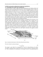
of the planar antenna. Figure 2 illustrates the final geometry of the printed antenna as well
as the Cartesian coordinate system.
Lsub
Wsub
r
w
f
L
g
g
x
y
z
Ground Plane
RT Duriod 5880
w
w
1
w
2
θ
h
2
h
1
h
Fig. 2. The geometry of the stepped-trapezoidal patch antenna
It consists of an isosceles trapezoidal patch with notch cut and two transition steps and a
partial finite-size ground plane. The Cartesian coordinate system (x,y,z) is oriented such that
the bottom surface of the substrate lies in the x-y plane. The antenna and the partial ground
plane are etched on opposite sides of the Rogers RT/Duroid 5880 substrate. The substrate
UWB(Ultrawideband)wirelesscommunications:UWBPrintedAntennaDesign 119
reff
L
W
Wh
GHz
f
)4(
904
)(
1
(2)
Where the effective relative permittivity ε
reff
can be calculated using:
2/)1(
rreff
(3)
Where
ε
r
: the relative permittivity of the substrate
Since the antenna is designed for UWB, it has to operate over 3.1 - 10.6 GHz. Therefore, the
lower edge frequency at which the initial parameters will be calculated is 3.1 GHz. Initially,
the antenna consists of an isosceles trapezoidal patch and partial ground plane etched on
opposite sides of the substrate. The radiator is fed through a microstrip line with 50-Ω
characteristic impedance. After setting up the configuration of the antenna, determining the
initial parameters and fixing the lower frequency, the simulation is started to confirm the
calculated parameters. Then, several bandwidth enhancement techniques are applied to
widen the bandwidth and to obtain the UWB performance. These techniques are: adjusting
the gap between radiating element and ground plane technique, using steps to control the
impedance stability and the notch cut technique. It used after studying the current
distribution and found out that the current distributions before and after the cut are
approximately the same. Also, the notch cut from the radiator is used to miniaturize the size
of the planar antenna. Figure 2 illustrates the final geometry of the printed antenna as well
as the Cartesian coordinate system.
Lsub
Wsub
r
w
f
L
g
g
x
y
z
Ground Plane
RT Duriod 5880
w
w
1
w
2
θ
h
2
h
1
h
Fig. 2. The geometry of the stepped-trapezoidal patch antenna
It consists of an isosceles trapezoidal patch with notch cut and two transition steps and a
partial finite-size ground plane. The Cartesian coordinate system (x,y,z) is oriented such that
the bottom surface of the substrate lies in the x-y plane. The antenna and the partial ground
plane are etched on opposite sides of the Rogers RT/Duroid 5880 substrate. The substrate
size of the proposed antenna is 30
×
30 mm
2
. The dimensions of isosceles trapezoidal patch
are w=28 mm, w
1
=20 mm and h=10.5 mm. The first transition step of w
1
×
h
1
= 20 mm × 2
mm and second transition step of w
2
×
h
2
= 14 mm × 3 mm are attached to the isosceles
trapezoidal patch. To reduce the overall size of the printed antenna and to get a better
impedance match, the circular-shaped notch with radius r =7 mm is symmetrically cut in the
top middle of the isosceles trapezoidal radiator. The shape of the partial ground plane is
selected to be rectangular with dimensions of 11
×
30 mm
2
. The radiator is fed through a
microstrip line having a length of 12 mm and width w
f
=3.6 mm to ensure 50-Ω characteristic
impedance with a feed gap of g = 1 mm.
6.3 Parametric study
The parametric study is carried out to optimize the antenna and provide more information
about the effects of the essential design parameters. The antenna performance is mainly
affected by geometrical and electrical parameters, such as the dimensions related to the notch
cut and the two transition steps.
(a) Notch cut
The circular-shaped notch cut is described by its radius and the location of its center. Both
parameters are studied. The effect of varying the notch radius on the impedance matching is
depicted in Figure 3. When the radius is increased, the entire band is highly affected, especially
the middle and higher frequencies experience higher mismatch levels. It is obviously
observed that the notch can be used to reduce the size of the radiator provided that the current
distribution has low density in the notch part. On the other hand, when the center of the notch
moves in the upper side of the patch, the entire band is slightly influenced. In general, the
notch cut parameters affect the impedance matching to a certain extent.
2 3 4 5 6 7 8 9 10 11 12
-35
-30
-25
-20
-15
-10
-5
0
fr
eque
n
cy,G
Hz
Return Loss,dB
r=4mm
r=6mm
r=7mm
r=9mm
r=11mm
Fig. 3. Effects of notch cut radius
(b) Transition steps
The effects of the two transition steps are studied. They have great impact on the matching
impedance for the whole band. For example, the effect of the width of the second step is
depicted in Figure 4. From the plot, the step width greatly affects the entire band, especially
at the high frequencies range, because the two steps influence the coupling between the
MobileandWirelessCommunications:Networklayerandcircuitleveldesign120
radiator and the ground plane. Thus, by adjusting the steps parameters, the impedance
bandwidth can be enhanced. In Figure 6, it is clear that a net improvement on the antenna
bandwidth is obtained when the two transitions steps are used.
2 3 4 5 6 7 8 9 10 11 12
-40
-35
-30
-25
-20
-15
-10
-5
0
fre
q
uenc
y
,GHz
Return Loss,dB
W2=8mm
W2=12mm
W2=14mm
W2=16mm
W2=20mm
Fig. 4. Effects of step width
6.4 Results and discussion
After taking into account the design considerations described on antenna structure, current
distributions and parametric study done to optimize the antenna geometry, the optimized
antenna is constructed as shown in Figure 5. Then, the antenna is experimentally tested to
confirm the simulation results. The simulated and measured return loss and radiation
patterns are presented. Also, the simulated gain is provided.
(a) Front view (b) Back view
Fig. 5. The prototype of the stepped-trapezoidal patch antenna
(a) Return loss
The return loss (S
11
) of the proposed antenna is measured. As depicted in Figure 6, the
measured and simulated results are shown for comparison and indicate a reasonable
agreement. In fact, the simulated return loss of the antenna is found to remain below -10 dB
beyond 12 GHz but that range of frequencies is omitted in Figure 6 since it is far out of the
allocated bandwidth for UWB communications under consideration. The measured -10 dB
return loss bandwidth of the antenna is approximately 8.7 GHz (3.13 - 11.83 GHz). Excellent
UWB(Ultrawideband)wirelesscommunications:UWBPrintedAntennaDesign 121
radiator and the ground plane. Thus, by adjusting the steps parameters, the impedance
bandwidth can be enhanced. In Figure 6, it is clear that a net improvement on the antenna
bandwidth is obtained when the two transitions steps are used.
2 3 4 5 6 7 8 9 10 11 12
-40
-35
-30
-25
-20
-15
-10
-5
0
fre
q
uenc
y
,GHz
Return Loss,dB
W2=8mm
W2=12mm
W2=14mm
W2=16mm
W2=20mm
Fig. 4. Effects of step width
6.4 Results and discussion
After taking into account the design considerations described on antenna structure, current
distributions and parametric study done to optimize the antenna geometry, the optimized
antenna is constructed as shown in Figure 5. Then, the antenna is experimentally tested to
confirm the simulation results. The simulated and measured return loss and radiation
patterns are presented. Also, the simulated gain is provided.
(a) Front view (b) Back view
Fig. 5. The prototype of the stepped-trapezoidal patch antenna
(a) Return loss
The return loss (S
11
) of the proposed antenna is measured. As depicted in Figure 6, the
measured and simulated results are shown for comparison and indicate a reasonable
agreement. In fact, the simulated return loss of the antenna is found to remain below -10 dB
beyond 12 GHz but that range of frequencies is omitted in Figure 6 since it is far out of the
allocated bandwidth for UWB communications under consideration. The measured -10 dB
return loss bandwidth of the antenna is approximately 8.7 GHz (3.13 - 11.83 GHz). Excellent
performance is obtained since the measured return loss is very close to the simulated one in
most range of the frequency band. The measured return loss shows that the antenna is
capable of supporting multiple resonance modes, which are closely distributed across the
spectrum. Therefore, the overlapping of these resonance modes leads to the UWB
characteristic.
2 3 4 5 6 7 8 9 10 11 12
-30
-25
-20
-15
-10
-5
0
frequency,GHz
Return Loss,d
B
Measured
Simulated
Fig. 6. The simulated & measured return loss
(b) Antenna radiation patterns
The radiation characteristics of the proposed antenna are also investigated. The two
dimensional radiation patterns presented here is taken at two sets of principal cuts, =0° and
=90°. Referring to the coordinate system attached to the antenna geometry in Figure 2, the
H-plane is the xz-plane and the E-plane is the yz-plane. Figures 7 and 8 illustrate the
simulated and measured H-plane and E-plane radiation patterns respectively at 3.5 and 9.5
GHz. In general, the simulated and measured results are fairly consistent with each other at
most of the frequencies but some discrepancies are noticed at higher frequencies, especially
in the E-plane. These discrepancies are most likely a result of the cable leakage current on
the coaxial cable that is used to feed the antenna prototype in the measurements [Kwon &
Kim, 2006]. This leakage current is known to be frequency sensitive as well. Also, intrinsic
noise within the anechoic chamber may contribute to these discrepancies.
Nevertheless, an analysis of the radiation pattern results shows that the proposed antenna is
characterized by omni-directional patterns in the H-plane for all in-band frequencies, as in
Figure 7. The measured H-plane patterns follow the shapes of the simulated ones well, except
at 9.5 GHz where there is little difference.
For the E-plane patterns, Figure 8 shows that they form a figure-of-eight pattern for
frequencies up to 7.5 GHz but at 9.5 GHz the shape changes. However, the measured E-
plane patterns generally follow the simulated ones well. In general, the stepped-trapezoidal
patch antenna shows an acceptable radiation pattern variation in its entire operational
bandwidth since the degradation happens only for a small part of the entire bandwidth and
it is not too severe.
MobileandWirelessCommunications:Networklayerandcircuitleveldesign122
(a) H-plane at 3.5 GHz (b) H-plane at 9.5 GHz
Fig. 7. The simulated and measured radiation patterns in the H-plane
(a) E-plane at 3.5 GHz (b) E-plane at 9.5 GHz
Fig. 8. The Simulated and measured radiation patterns in the E-plane
(c) Antenna gain
The gain of the proposed antenna is also found to be suitable for the UWB communications
and applications. It is greater than 2.9 dBi for all in-band frequencies and varies from 2.9 dBi
to 5.2 dBi over the operating frequency range, resulting in the maximum gain variation of
2.3 dB.
7. The Double-Beveled Patch Antenna
7.1 Overview
A novel planar patch antenna with a notch-cut fed by a simple microstrip line is proposed
and described. It is designed and fabricated for UWB wireless communications and
applications under the band (3.1-10.6 GHz). This antenna is composed of a symmetrical
double-beveled planar patch antenna with notch cut fed by a microstrip line folded on a
partial ground plane. Because of its structure, we have called it “the Double-Beveled Patch
-30
-20
-10
0
60
120
30
150
0
180
30
150
60
120
90
90
__ Measured
Simulated
-30
-20
-10
0
60
120
30
150
0
180
30
150
60
120
90
90
__ Measured
Simulated
-30
-20
-10
0
60
120
30
150
0
180
30
150
60
120
90
90
__ Measured
Simulated
-30
-20
-10
0
60
120
30
150
0
180
30
150
60
120
90
90
__ Measured
Simulated
UWB(Ultrawideband)wirelesscommunications:UWBPrintedAntennaDesign 123
(a) H-plane at 3.5 GHz (b) H-plane at 9.5 GHz
Fig. 7. The simulated and measured radiation patterns in the H-plane
(a) E-plane at 3.5 GHz (b) E-plane at 9.5 GHz
Fig. 8. The Simulated and measured radiation patterns in the E-plane
(c) Antenna gain
The gain of the proposed antenna is also found to be suitable for the UWB communications
and applications. It is greater than 2.9 dBi for all in-band frequencies and varies from 2.9 dBi
to 5.2 dBi over the operating frequency range, resulting in the maximum gain variation of
2.3 dB.
7. The Double-Beveled Patch Antenna
7.1 Overview
A novel planar patch antenna with a notch-cut fed by a simple microstrip line is proposed
and described. It is designed and fabricated for UWB wireless communications and
applications under the band (3.1-10.6 GHz). This antenna is composed of a symmetrical
double-beveled planar patch antenna with notch cut fed by a microstrip line folded on a
partial ground plane. Because of its structure, we have called it “the Double-Beveled Patch
-30
-20
-10
0
60
120
30
150
0
180
30
150
60
120
90
90
__ Measured
Simulated
-30
-20
-10
0
60
120
30
150
0
180
30
150
60
120
90
90
__ Measured
Simulated
-30
-20
-10
0
60
120
30
150
0
180
30
150
60
120
90
90
__ Measured
Simulated
-30
-20
-10
0
60
120
30
150
0
180
30
150
60
120
90
90
__ Measured
Simulated
Antenna” [Alshehri & Sebak, 2008]. To obtain UWB bandwidth, we use several bandwidth
enhancement techniques: the use of partial ground plane, adjusting the gap between
radiating element and a ground plane technique, the use of bevels technique and a notch cut
technique used also to reduce the size of the planar antenna. A parametric study is
numerically carried out on the important geometrical parameters to understand their effects
on the proposed antenna and therefore optimize its performance. The measured -10 dB
return loss (VSWR<2) bandwidth is about 123.8% (9.74 GHz). The proposed antenna
provides an acceptable radiation pattern and a relatively flat gain over the entire frequency
band. The measured and simulated results for both bandwidth and radiation pattern show a
very reasonable agreement. In the following subsections, the design details and the related
results are presented and discussed.
7.2 Antenna design
First, the substrate is chosen to be Rogers RT/Duroid 5880 material with a relative
permittivity ε
r
= 2.2 and a thickness of 1.575 mm. Second, the radiator shape is selected to be
rectangular. Next, the initial parameters are calculated using the empirical formula reported
in [Agrawall, et al., 1998] after adding the effect of the substrate:
It is found that the frequency corresponding to the lower edge of the bandwidth of the
monopole antenna can be predicted approximately by equating the area of the planar
configuration to that of a cylindrical wire and given by:
hWrl
2
(4)
So, the resonant frequency is given by:
r
l
c
GHz
f
L
24.030
)(
(5)
Where:
f
L
: the frequency corresponding to the lower edge of the bandwidth.
C: the light speed.
: the wavelength
l: the height of the cylindrical wire which is same as that of planar configuration height
r: the equivalent radius of the cylindrical wire
W: the width of the rectangular patch.
h: the height of the rectangular patch.
The dimensions are expressed in centimeters. This simple formula is used to predict the
lower edge frequency of the bandwidth for the monopole suspended in the space over the
ground plane. It is accurate to +/- 8 %. In our design, the sheet will be a patch printed on the
substrate, so, the effect of the substrate has to be included to the formula. After consideing it,
the formula becomes:
reff
L
rl
GHz
f
)(
24.030
)(
(6)
MobileandWirelessCommunications:Networklayerandcircuitleveldesign124
where the effective relative permittivity ε
reff
can be calculated using Equation 3.
Since the antenna is designed for UWB, it has to operate over 3.1 - 10.6 GHz. Therefore, the
lower edge frequency at which the initial parameters will be calculated is 3.1 GHz. Initially,
the antenna consists of a rectangular patch and partial ground plane etched on opposite
sides of the substrate. The radiator is fed through a microstrip line with 50-Ω characteristic
impedance. After setting up the configuration of the antenna, determining the initial
parameters and fixing the lower frequency, the simulation is performed to confirm the
calculated parameters. Then, several bandwidth-enhancement techniques are applied to
widen the bandwidth and obtain UWB performance. These techniques are: adjusting the
gap between radiating element and ground plane technique, the bevels technique and notch
cut technique used after studying the current distribution as will be discussed later.
Figure 9 illustrates the geometry of the printed antenna as well as the Cartesian coordinate
system. It consists of a symmetrical double-beveled patch with notch cut and a partial
ground plane. The Cartesian coordinate system (x,y,z) is oriented such that the bottom
surface of the substrate lies in the x-y plane. The antenna and the partial ground plane are
oppositely etched on the Rogers RT/Duroid 5880 substrate. The substrate size of the
proposed antenna is 40
×
31 mm
2
.
L
sub
W
sub
w
f
L
g
g
Ground Plan
e
x
y
z
RT Duriod 5880
θ
2
θ
1
l
s
w
s
ww
h
Fig. 9. The geometry of the double-beveled patch antenna
The parameters of the symmetrical double-beveled patch are w=6.5 mm, h=12 mm, θ
1
=17.5
○
(the angle of the first bevel) and θ
2
=45
○
(the angle of the second bevel). To reduce the overall
size of the printed antenna and to get better impedance matching, a rectangular-shaped
notch with dimensions of
l
s
×
w
s
= 8 mm × 10 mm is symmetrically cut in the top middle of
the radiator. The shape of the partial ground plane is rectangular with dimensions of 10
×
40
mm
2
. The radiator is fed through a microstrip line having a length of 10.5 mm and width w
f
=3.6 mm to ensure 50-Ω input impedance with a feed gap of g = 0.5 mm. The 50 -microstrip
line is printed on the same side of the substrate as the radiator.
UWB(Ultrawideband)wirelesscommunications:UWBPrintedAntennaDesign 125
where the effective relative permittivity ε
reff
can be calculated using Equation 3.
Since the antenna is designed for UWB, it has to operate over 3.1 - 10.6 GHz. Therefore, the
lower edge frequency at which the initial parameters will be calculated is 3.1 GHz. Initially,
the antenna consists of a rectangular patch and partial ground plane etched on opposite
sides of the substrate. The radiator is fed through a microstrip line with 50-Ω characteristic
impedance. After setting up the configuration of the antenna, determining the initial
parameters and fixing the lower frequency, the simulation is performed to confirm the
calculated parameters. Then, several bandwidth-enhancement techniques are applied to
widen the bandwidth and obtain UWB performance. These techniques are: adjusting the
gap between radiating element and ground plane technique, the bevels technique and notch
cut technique used after studying the current distribution as will be discussed later.
Figure 9 illustrates the geometry of the printed antenna as well as the Cartesian coordinate
system. It consists of a symmetrical double-beveled patch with notch cut and a partial
ground plane. The Cartesian coordinate system (x,y,z) is oriented such that the bottom
surface of the substrate lies in the x-y plane. The antenna and the partial ground plane are
oppositely etched on the Rogers RT/Duroid 5880 substrate. The substrate size of the
proposed antenna is 40
×
31 mm
2
.
L
sub
W
sub
w
f
L
g
g
Ground Plan
e
x
y
z
RT Duriod 5880
θ
2
θ
1
l
s
w
s
ww
h
Fig. 9. The geometry of the double-beveled patch antenna
The parameters of the symmetrical double-beveled patch are w=6.5 mm, h=12 mm, θ
1
=17.5
○
(the angle of the first bevel) and θ
2
=45
○
(the angle of the second bevel). To reduce the overall
size of the printed antenna and to get better impedance matching, a rectangular-shaped
notch with dimensions of
l
s
×
w
s
= 8 mm × 10 mm is symmetrically cut in the top middle of
the radiator. The shape of the partial ground plane is rectangular with dimensions of 10
×
40
mm
2
. The radiator is fed through a microstrip line having a length of 10.5 mm and width w
f
=3.6 mm to ensure 50-Ω input impedance with a feed gap of g = 0.5 mm. The 50 -microstrip
line is printed on the same side of the substrate as the radiator.
7.3 Current distribution
The current distribution is studied. The simulated current distributions of the initial antenna
geometry before cutting the region of low current density at 3.5 and 9.5 GHz (as examples)
are shown in Figure 10 (a) and (b) respectively. The current is mainly concentrated on the
bottom portion of the patch with very low density toward and above the center and it is
distributed along the edges of the patch, except the top edge, for all frequencies. Thus, it can
conclude that the region of low current density on the patch is not that important in the
antenna performance and could therefore be cut out. Consequently, a rectangular section
with dimensions of
l
s
×
w
s
= 8 mm × 10 mm is symmetrically cut out from the top middle of
the rectangular radiator to eliminate a region of low current density as shown in Figure 9.
After this cut, the current distributions at 3.5 GHz and 9.5 GHz (as examples) are depicted in
Figure 10 (c) and (d), respectively. It is observed that the current distributions in this case are
approximately the same as before the cut. As a result of this cut, the size of the antenna is
reduced and has lighter weight, which is very desirable for more degree of freedom in
design and possibly less conductor losses.
(a) at 3.5 GHz (c) at 3.5 GHz
(b) at 9.5 GHz (d) at 9.5 GHz
Fig. 10. The current distributions
7.4 Parametric study
The parametric study is done to optimize the antenna. Its performance is mainly affected by
geometrical parameters, such as the dimensions related to the notch cut and the bevels.
MobileandWirelessCommunications:Networklayerandcircuitleveldesign126
(a) Notch cut
The effect of the rectangular-shaped notch dimensions (
l
s
,
w
s
) on the return loss is
studied. It is observed that the width of the notch has a major effect on the impedance
matching over the entire frequency range, as shown in Figure 11. The lower edge frequency of
the bandwidth is shifted to higher frequencies once the width increases. Also, the middle and
higher frequencies are affected with higher mismatch levels. On the other hand, the length of
the notch slightly influences the lower edge frequency. It is also observed that the notch can be
used to reduce the size of the radiator, as explained earlier using the current distribution.
1 2 3 4 5 6 7 8 9 10 11 12
-35
-30
-25
-20
-15
-10
-5
0
frequency,GHz
Return Loss,dB
Ws=5mm
Ws=10mm,Opt
Ws=18mm
Ws=21mm
Fig. 11. Effects of the width of notch cut
(b) Bevels
The double bevels dimensions influence the matching impedance for the whole band,
especially at high frequencies. The high frequencies can be controlled and the entire band
can be enhanced by adjusting the bevel angles. By varying the angle of the first bevel (θ
1
), the
low and middle frequencies are highly influenced. As shown in Figure 12, by varying the
angle of the second bevel (θ
2
), the whole band is affected especially at middle and high
frequencies. Thus, using two progressive bevels provides more degree of freedom and by
adjusting them, the bandwidth will be widened as well as excellent level of matching can be
achieved.
1 2 3 4 5 6 7 8 9 10 11 12
-30
-25
-20
-15
-10
-5
0
frequency,GHz
Return Loss,dB
25
30
45,Opt
65
Fig. 12. Effects of second bevel angle
UWB(Ultrawideband)wirelesscommunications:UWBPrintedAntennaDesign 127
(a) Notch cut
The effect of the rectangular-shaped notch dimensions (
l
s
,
w
s
) on the return loss is
studied. It is observed that the width of the notch has a major effect on the impedance
matching over the entire frequency range, as shown in Figure 11. The lower edge frequency of
the bandwidth is shifted to higher frequencies once the width increases. Also, the middle and
higher frequencies are affected with higher mismatch levels. On the other hand, the length of
the notch slightly influences the lower edge frequency. It is also observed that the notch can be
used to reduce the size of the radiator, as explained earlier using the current distribution.
1 2 3 4 5 6 7 8 9 10 11 12
-35
-30
-25
-20
-15
-10
-5
0
frequency,GHz
Return Loss,dB
Ws=5mm
Ws=10mm,Opt
Ws=18mm
Ws=21mm
Fig. 11. Effects of the width of notch cut
(b) Bevels
The double bevels dimensions influence the matching impedance for the whole band,
especially at high frequencies. The high frequencies can be controlled and the entire band
can be enhanced by adjusting the bevel angles. By varying the angle of the first bevel (θ
1
), the
low and middle frequencies are highly influenced. As shown in Figure 12, by varying the
angle of the second bevel (θ
2
), the whole band is affected especially at middle and high
frequencies. Thus, using two progressive bevels provides more degree of freedom and by
adjusting them, the bandwidth will be widened as well as excellent level of matching can be
achieved.
1 2 3 4 5 6 7 8 9 10 11 12
-30
-25
-20
-15
-10
-5
0
frequency,GHz
Return Loss,dB
25
30
45,Opt
65
Fig. 12. Effects of second bevel angle
7.5 Results and discussion
After taking into account the design considerations described on antenna structure, current
distributions and parametric study done to optimize the antenna geometry, the optimized
antenna is constructed as shown in Figure 13 using the optimum values as mentioned
earlier . Then, the antenna is experimentally tested to confirm the simulation results. The
simulated and measured VSWR is presented as well as the simulated and measured radiation
patterns in principle planes. Also, the simulated gain is provided.
(a) Front view (b) Back view
Fig. 13. The prototype of the double-beveled patch antenna
(a) VSWR
The VSWR of the proposed antenna is measured as depicted in Figure 14. The measured -10
dB return loss (VSWR<2) bandwidth of the antenna is approximately 9.74 GHz (3.00-12.74
GHz) and the antenna shows stable behaviors over the band. Thus, the measurement
confirms the UWB characteristic of the double-beveled patch antenna as predicted in the
simulation.
1 2 3 4 5 6 7 8 9 10 11 12 13
1
2
3
4
5
6
7
8
9
10
frequency GHz
VSWR
Measured
Simulated
Fig. 14. Simulated & measured VSWR
(b) Antenna radiation patterns
The radiation characteristics of the proposed antenna are also investigated. Figures 15 and
16 illustrate the simulated and measured H-plane and E-plane radiation patterns
MobileandWirelessCommunications:Networklayerandcircuitleveldesign128
respectively at 3.5, 5.5, 7.5 and 9.5 GHz. In genral, the simulated and measured results are
fairly consistent at most of the frequencies but some discrepancies are noticed at higher
frequencies especially in the E-plane. Nevertheless, the proposed antenna is characterized
by omni-directional patterns in the H-plane for all in-band frequencies as in Figure 15. For
the E-plane patterns, Figure 16 shows that the simulated ones at low frequencies form
figure-of-eight patterns but at high frequencies, there are dips, especially at 9.5 GHz. In
general, the double-beveled patch antenna shows an acceptable radiation pattern variation
in its whole operational bandwidth since the degradation happens only for a small part of
the entire bandwidth and it is not too drastic.
(a) H-plane at 3.5GHz (b) H-plane at 5.5GHz
(c) H-plane at 7.5GHz (d) H-plane at 9.5GHz
Fig. 15. The simulated and measured radiation patterns in the H-plane
-30
-20
-10
0
60
120
30
150
0
180
30
150
60
120
90
90
__ Measured
Simulated
-30
-20
-10
0
60
120
30
150
0
180
30
150
60
120
90
90
__ Measured
Simulated
-30
-20
-10
0
60
120
30
150
0
180
30
150
60
120
90
90
__ Measured
Simulated
-30
-20
-10
0
60
120
30
150
0
180
30
150
60
120
90
90
__ Measured
Simulated
UWB(Ultrawideband)wirelesscommunications:UWBPrintedAntennaDesign 129
respectively at 3.5, 5.5, 7.5 and 9.5 GHz. In genral, the simulated and measured results are
fairly consistent at most of the frequencies but some discrepancies are noticed at higher
frequencies especially in the E-plane. Nevertheless, the proposed antenna is characterized
by omni-directional patterns in the H-plane for all in-band frequencies as in Figure 15. For
the E-plane patterns, Figure 16 shows that the simulated ones at low frequencies form
figure-of-eight patterns but at high frequencies, there are dips, especially at 9.5 GHz. In
general, the double-beveled patch antenna shows an acceptable radiation pattern variation
in its whole operational bandwidth since the degradation happens only for a small part of
the entire bandwidth and it is not too drastic.
(a) H-plane at 3.5GHz (b) H-plane at 5.5GHz
(c) H-plane at 7.5GHz (d) H-plane at 9.5GHz
Fig. 15. The simulated and measured radiation patterns in the H-plane
-30
-20
-10
0
60
120
30
150
0
180
30
150
60
120
90
90
__ Measured
Simulated
-30
-20
-10
0
60
120
30
150
0
180
30
150
60
120
90
90
__ Measured
Simulated
-30
-20
-10
0
60
120
30
150
0
180
30
150
60
120
90
90
__ Measured
Simulated
-30
-20
-10
0
60
120
30
150
0
180
30
150
60
120
90
90
__ Measured
Simulated
(a) E-plane at 3.5GHz (b) E-plane at 9.5GHz
Fig. 16. The simulated and measured radiation ratterns in the E-plane
(c) Antenna gain
The gain versus frequency of the proposed antenna is also found to be suitable for the UWB
communications and applications. The simulated antenna gain versus frequency is shown in
Figure 17. It is greater than 3.4 dBi for all in-band frequencies and varies from 3.4 dBi to 6.1
dBi over the operating frequency range, resulting in the maximum gain variation of 2.7 dB.
3 4 5 6 7 8 9 10
0
1
2
3
4
5
6
7
8
frequency,GHz
Gain,dBi
Fig. 17. Simulated gain
8. Conclusion
An overview on Ultra Wideband wireless communications is given. Two novel, small, low-
profile, microstrip-fed printed UWB antennas are analyzed, designed and implemented to
satisfy UWB technology requirements. The focus is on UWB frequency domain characteristics
such as the far field radiation patterns, bandwidth and gain. The antenas provide excellent
performance in the entire operational bandwidth. Because of their low cost, light weight and
ease of implementation, these printed designs are desired in UWB wireless communication
systems and applications, especially in portable devices and indoor applications such as
WPAN. These antennas are namely: the stepped-trapezoidal patch antenna and the double-
-30
-20
-10
0
60
120
30
150
0
180
30
150
60
120
90
90
__ Measured
Simulated
-30
-20
-10
0
60
120
30
150
0
180
30
150
60
120
90
90
__ Measured
Simulated
MobileandWirelessCommunications:Networklayerandcircuitleveldesign130
beveled patch antenna. Both provides a nearly omni-directional radiation pattern and a
relatively flat gain over the entire frequency band with a maximum variation of 2.3 dB for
first one and 2.7 dB for the second one. Both antennas offer reduced patch size, more degree
of freedom for design, extra space that could accommodate other RF circuit elements.
However, the effect Analysis of the notch cut show that within a certain limit of the cutout
size, the radiation properties do not change drastically. But beyond that limit, the notch cut
highly affects radiation patterns in the entire operational bandwidth.
UWB systems occupy huge operational bandwidth and often utilize very short pulses for
data transmission. Therefore, an appropriate time domain performance is a key requirement
for UWB antennas. Accordingly, investigations and analysis will be carried out on the effect
of the proposed antennas on the transmitted pulse to hence improve the time domain
behavior by optimizing the antenna designs.
9. References
Agrawall, N.; Kumar, G. & Ray, K. (1998). Wide-Band Planar Monopole Antennas, IEEE
Transactions on Antennas and Propagation, vol. 46, No., February 1998, (294-295),
0018-926X
Alshehri A. (2008). Novel Ultra Wideband Antennas for Wireless Systems, M. A. Sc. Thesis,
Concordia University, Canada
Alshehri, A. & Sebak, A. (2008). A Novel UWB Planar Patch Antenna for Wireless
Communications, IEEE International Symposium on Antennas and Propagation, pp. 1-
4, 978-1-4244-2041-4, USA, July 2008, IEEE, San Diego
Alshehri,A.; Sebak, A. & Denidni, T. (2008). A Novel UWB Stepped-Trapezoidal Patch
Antenna for Wireless Communications, The IASTED International Conference on
Antennas, Radar and Wave Propagation (ARP 2008),pp. 27-31, 978-0-88986-735-2, USA,
April 2008, ACTA Press, Calgary
Ammann, M. & Chen, Z. (2003). A Wide-Band Shorted Planar Monopole with Bevel, IEEE
Transactions on Antennas and Propagation, Vol. 51, No.4, April 2003, (901-903), 0018-
926X
Ammann, M. & Chen, Z. (2004). An Asymmetrical Feed Arrangement for Improved
Impedance Bandwidth of Planar Monopole Antennas, Microwave and Optical
Technology Letters, Vol. 40, No. 2, January 2004, (156-158)
Ammann, M. & Chen, Z. (2003). Wideband Monopole Antennas for Multi-Band Wireless
Systems, IEEE Antennas and Propagation Magazine, vol. 45, No. 2, April 2003, (146-
150), 1045-9243
Ammann, M. (2001), Control of the Impedance Bandwidth of Wideband Planar Monopole
Antennas Using A Beveling Technique, Microwave and Optical Technology Letters,
Vol. 30, No. 2July 2001, (229-232)
Arslan, H.; Chen, Z. & Benedetto, M. (2006). Ultra Wideband Wireless Communication, John Wiley
& Sons, Inc., 0471715212, New Jersey
Azenui, N. (2007). Miniaturized Printed Circuit Antennas for Multi- and Ultra-Wide Band
Applications, PHD Thesis, University of Illinois, USA
Balanis, C. (2005). Antenna Theory Analysis and Design, John Wiley & Sons, Inc., 047166782X,
New Jersey
UWB(Ultrawideband)wirelesscommunications:UWBPrintedAntennaDesign 131
beveled patch antenna. Both provides a nearly omni-directional radiation pattern and a
relatively flat gain over the entire frequency band with a maximum variation of 2.3 dB for
first one and 2.7 dB for the second one. Both antennas offer reduced patch size, more degree
of freedom for design, extra space that could accommodate other RF circuit elements.
However, the effect Analysis of the notch cut show that within a certain limit of the cutout
size, the radiation properties do not change drastically. But beyond that limit, the notch cut
highly affects radiation patterns in the entire operational bandwidth.
UWB systems occupy huge operational bandwidth and often utilize very short pulses for
data transmission. Therefore, an appropriate time domain performance is a key requirement
for UWB antennas. Accordingly, investigations and analysis will be carried out on the effect
of the proposed antennas on the transmitted pulse to hence improve the time domain
behavior by optimizing the antenna designs.
9. References
Agrawall, N.; Kumar, G. & Ray, K. (1998). Wide-Band Planar Monopole Antennas, IEEE
Transactions on Antennas and Propagation, vol. 46, No., February 1998, (294-295),
0018-926X
Alshehri A. (2008). Novel Ultra Wideband Antennas for Wireless Systems, M. A. Sc. Thesis,
Concordia University, Canada
Alshehri, A. & Sebak, A. (2008). A Novel UWB Planar Patch Antenna for Wireless
Communications, IEEE International Symposium on Antennas and Propagation, pp. 1-
4, 978-1-4244-2041-4, USA, July 2008, IEEE, San Diego
Alshehri,A.; Sebak, A. & Denidni, T. (2008). A Novel UWB Stepped-Trapezoidal Patch
Antenna for Wireless Communications, The IASTED International Conference on
Antennas, Radar and Wave Propagation (ARP 2008),pp. 27-31, 978-0-88986-735-2, USA,
April 2008, ACTA Press, Calgary
Ammann, M. & Chen, Z. (2003). A Wide-Band Shorted Planar Monopole with Bevel, IEEE
Transactions on Antennas and Propagation, Vol. 51, No.4, April 2003, (901-903), 0018-
926X
Ammann, M. & Chen, Z. (2004). An Asymmetrical Feed Arrangement for Improved
Impedance Bandwidth of Planar Monopole Antennas, Microwave and Optical
Technology Letters, Vol. 40, No. 2, January 2004, (156-158)
Ammann, M. & Chen, Z. (2003). Wideband Monopole Antennas for Multi-Band Wireless
Systems, IEEE Antennas and Propagation Magazine, vol. 45, No. 2, April 2003, (146-
150), 1045-9243
Ammann, M. (2001), Control of the Impedance Bandwidth of Wideband Planar Monopole
Antennas Using A Beveling Technique, Microwave and Optical Technology Letters,
Vol. 30, No. 2July 2001, (229-232)
Arslan, H.; Chen, Z. & Benedetto, M. (2006). Ultra Wideband Wireless Communication, John Wiley
& Sons, Inc., 0471715212, New Jersey
Azenui, N. (2007). Miniaturized Printed Circuit Antennas for Multi- and Ultra-Wide Band
Applications, PHD Thesis, University of Illinois, USA
Balanis, C. (2005). Antenna Theory Analysis and Design, John Wiley & Sons, Inc., 047166782X,
New Jersey
Barrett, T. (2000). History of Ultra Wideband (UWB) Radar & Communications: Pioneers and
Innovators,” Progress in Electromagnetics Symposium 2000, USA, July 2000.
Bataller, M.; Fabrés, M.; Daviu E. et al. (2006). Overview of Planar Monopole Antennas for
UWB Applications, Proceeding of EUCAP 2006, ESA SP-626, November 2006, France
Bhartia, P.; Bahl, I.; Garg, R.; et al. (2000). Microstrip Antenna Design Handbook, Artech House,
0890065136, USA
Cai, A.; See, T. & Chen, Z. (2005). Study of Human Head Effects on UWB Antenna, IEEE
International Workshop on Antenna Technology (iWAT), 0-7803-8842-9, March 2005,
pp. 310–313, IEEE
Chen, D. & Chen, H. (2004). A CPW-Fed Dual-Frequency Monopole Antenna, IEEE
Transactions on Antennas and Propagation, vol. 52, No. 4, April 2004, (978-982), 0018-
926X
Chen, Z.; Ammann, M. & Chia, M. (2003). Broadband Square Annular Planar Monopoles,”
Microwave and Optical Technology Letters, vol. 36, No. 6, March 2003, (449-454)
Chen, Z.; Ammann, M.; Qing X., et al. (2006). Planar Antennas, IEEE Microwave Magazine,
Vol. 7, No. 6, December 2006, (63-73), 1527-3342
Chen, Z.; See, T. & Qing, X. (2007). Small Printed Ultra Wideband Antenna with Reduced
Ground Plane Effect, IEEE Transactions on Antennas and Propagation, vol. 55, No. 3
February 2007, (383-388), 0018-926X
Choi, S.; Lee, H. & Kwak, K. (2006). Clover-Shaped Antenna for Ultra-Wideband
Communications, Microwave and Optical Technology Letters, Vol. 48, No. 10, July 2006
(2111-2113).
Choi, S.; Park, J.; Kim, S. et al. (2004). A New Ultra-Wideband Antenna for UWB
Applications, Microwave and Optical Technology Letters, Vol. 40. No. 5, March 2004,
(399-401)
Daviu, E.; Fabres, M.; Bataller, M. et al. (2003). Wideband Double-Fed Planar Monopole
Antennas, Electronics Letters, Vol. 39, November 2003, (1635-1636), 0013-5194
Dotto, K. (2005) Development of a Novel Ultra-Wideband Antenna and Prototype Scanner for
Detection and Location of Voids in Wood, PHD Thesis, The University of British
Columbia
Dyson, J. (1959). The Unidirectional Equiangular Spiral Antenna, IEEE Transactions on
Antennas Propagation, Vol. 7, No. 4, October 1959, (329-334), 0096-1973
Evans, J.; Amunann, M. (1999), Planar Trapezoidal and Pentagonal Monopoles with
Impedance Bandwidths in Excess of 10:1, IEEE International Antenna and Propagation
Symposium, pp.1558-1561, 0-7803-5639-x, Orlando, FL, July 1999, IEEE, Orlando
Federal Communication Commission (2002). First Report and Order, Revision of Part 15 of the
Commission’s Rules Regarding Ultra-Wideband Transmission System, FCC 02 48
HFSS
TM
, v10, Ansoft Corporation Software, Pittsburgh, PA, USA
Huang, C. & Hsia, W. (2005). Planar Elliptical Antenna for Ultrawideband Communications,
Electronics Letters, Vol. 41, No. 6, March 2005, (296-297), 0013-5194
Kwon, D. & Kim, Y. (2006). Suppression of Cable Leakage current for Edge-Fed Printed
Dipole UWB Antennas Using Leakage-Blocking Slots, IEEE Antennas and Wireless
Propagation Letters, vol. 5, No. 1 ,December 2006, (183-186), 1536-1225
Lee, S.; Park, J. & Lee J. (2005). A Novel CPW-Fed Ultra-Wideband Antenna Design,
Microwave Optical Technology Letters, Vol. 44, No. 5, January 2005, (393-396)
MobileandWirelessCommunications:Networklayerandcircuitleveldesign132
Lee, E.; Hall, P. & Gardner, P. (1999). Compact Wideband Planar Monopole Antenna,
Electronics Letters, Vol. 35, December 1999, (2157-2158), 0013-5194
Lee, F.; Wentzloff,D. & Chandrakasan, A. (2004). An Ultra-Wideband Baseband Front-End,
IEEE Radio Frequency Integrated Circuits (RFIC) Symposium, pp.493-496, 0-7803-8333-
8, USA, June 2004, IEEE, Cambridge
Liang, J. (2006). Antenna Study and Design for Ultra Wideband Communication Applications,
PHD Thesis, University of London, United Kingdom
Lu, G. (2006). Antenna and Synchronization Design Issues for the Ultra-Wideband Systems, PHD
Thesis, the State University of New Jersey, USA,
Muscat, A. & Parini, C. (2001). Novel Compact Handset Antenn, IEEE 11
th
International
Conference on Antennas and Propagation, pp. 336-339, 0-85296-733-0, Manchester, UK,
April 2001, IEEE
Oppermann, I.; Hamalainen, M. & Iinatti, J. (2004). UWB Theory and Applications, John Wiley
& Sons, Ltd, 0470869178, New Jersey
Powell, J. (2004). Antenna Design for Ultra Wideband Radio, M. A. Sc. Thesis, Massachusetts
Institute of Technology, USA
Ross, G. (1968). A Time Domain Criterion for the Design of Wideband Radiating Elements,
IEEE Transactions on Antennas Propagation, vol. 16, No. 3, May 1968, (355- 356), 0018-
926X
Ross, G. (1973). Transmission and Reception System for Generating and Receiving Base-Band
Duration Pulse Signals for Short Base-Band Pulse Communication System, April
1973, U.S. Patent no. 3728632
Rudge, A.; Milne, K.; Olver, A.; (1982). The Handbook of Antenna Design, Peter Peregrinus
Ltd., 0906048826, UK
Rumsey, V. (1957). Frequency Independent Antennas, IRE National Convention Record, Vol. 5,
March 1957, (114-118)
Sadiku, M. (2009). Numerical Techniques in Electromagnetics, CRC Press LLC., 142006309X
USA
Schantz, H. (2003). A Brief History of Ultra-Wideband Antennas, IEEE Conference on
UWBST, pp. 209-213, 0-7803-8187-4, November 2003
Siriwongpairat, W. (2005). Cross-Layer Design for Multi-Antenna Ultra-Wideband Systems, PHD
Thesis, University of Maryland, USA
Siwiak, K. & McKeown, D. (2004) Ultra-Wideband Radio Technology, John Wiley & Sons, Ltd.,
0470859318, New Jersey
Tsai, M. & Wang, H. (2004). A 0.3-25 GHz Ultra-Wideband Mixer Using Commercial 0.18-
/μm CMOS Technology, IEEE Microwave and Wireless Components Letters, Vol. 14,
No. 14 November 2004, (522-524), 1531-1309
Wentzloff, D.; Blazquez R. ; Lee F. , et al. (2005), System Design Considerations for Ultra-
Wideband Communication, IEEE Communications magazine, Vol. 43, August 2005,
(114-121), 0163-6804
Wong, K.; Chi, Y.; Su C.; et al. (2005). Band-Notched Ultra-Wideband Circular-Disc
Monopole Antenna with an Arc-Shaped Slot, Microwave and Optical Technology
Letters, vol. 45, No. 3, May 2005, (188-191)
Yang, L.; Giannakis, G. (2004). Ultra-Wideband Communications: An Idea Whose Time Has
Come, IEEE Signal Processing Magazine, Vol. 21, No. 6, November 2004, (26-54),
1053-5888
Micromachinedhighgainwidebandantennasforwirelesscommunications 133
Micromachinedhighgainwidebandantennasforwirelesscommunications
SumanthK.Pavuluri,ChanghaiWangandAlanJ.Sangster
X
Micromachined high gain wideband
antennas for wireless communications
Sumanth K. Pavuluri, Changhai Wang and Alan J. Sangster
Heriot Watt University
Edinburgh, EH14 4AS, UK
1. Introduction
The seemingly insatiable and growing demand for compact, multi-function, multi-frequency
electronic systems for communications and other applications, is continuing to drive the
search for devices offering more and more bandwidth. There is growing need for broadband
high gain communication systems in the X band range of frequencies (8 - 12 GHz) for
terrestrial broadband communications and networking as well as for radar applications.
Similarly, direct broadcast satellite (DBS) and various other applications in the K
u
band (10 -
14 GHz) such as radio astronomy service, space research service, mobile service, mobile
satellite service, radio location service (radar), amateur radio service, and radio navigation
may require embedded antenna systems at different bands. It would be ideal if efficient,
broadband and cost effective planar microstrip based antenna and antenna array devices
could be designed to provide coverage of all these bands. In addition systems aimed at
UWB (Ultra Wide Band) operation need efficient very wideband antenna devices.
For these high frequency systems, compact size and high performance can usually be
achieved by fabricating the antenna onto a low dielectric constant material and integrating it
with the remaining circuitry implemented on a high dielectric constant substrate in
neighbouring regions in the same package. This trend has serious implications for antennas,
where these are required to be embedded within the system package, such as a mobile
phone. Systems operating in the microwave and millimetre-wave frequency bands offer the
possibility of high levels of integration of individual devices in high density layouts. The
most compact circuit designs are invariably achieved by employing high dielectric constant
substrates, but this is a requirement which is essentially incompatible with the needs of an
embedded planar antenna. Such antennas radiate most efficiently when fabricated onto
substrates which exhibit low dielectric constant (Papapolymerou et al., 1998). While it is not
impossible to fabricate microstrip or coplanar circuits, together with planar antennas on the
same high permittivity silicon substrate, antenna gain and efficiency will inevitably be very
poor.
Various schemes have been suggested, in recent years, aimed at overcoming the opposing
substrate requirements of circuits and antennas. These largely involve the use of layered
materials with high and low permittivities in adjacent layers (Chen, 2008). However such
8
MobileandWirelessCommunications:Networklayerandcircuitleveldesign134
methods tend to be of quite limited versatility and the trend now is toward selective
removal of substrate in the vicinity of the antenna. This can be done by, for example, bulk
micromachining an air gap between the planar antenna (usually a conducting patch) and the
ground plane (Koul, 2007). The advantages of doing so are as follows:
Lower effective dielectric constant, hence wider circuit dimensions
Ease of fabrication and relaxed dimensional tolerances
Lower attenuation
Enhanced radiation efficiency in case of antennas
Eliminating surface waves
Micromachining technology continues to develop, and it is being applied in new ways to
embedded antennas to improve their performance. The use of selective lateral etching based
on micromachining techniques to enhance the performance of rectangular microstrip patch
antennas printed on high-index wafers such as silicon, GaAs, and InP have been developed
in the past decade. A novel polymer micromachining based method for achieving high
performance, cost effective antennas is described in this chapter.
2. Micromachined antennas
Over the last decade several micromachining techniques have been developed for
producing microwave wave and millimeter wave antennas. Devices using these procedures
have achieved high performances compared to the conventional patches printed on to
relatively high dielectric constant substrates. Various micromachining methods that have
been implemented recently are listed in the following sections.
2.1 Silicon micromachining
Silicon micromachining has been employed to fabricate a patch antenna wherein, the silicon
material was removed laterally underneath it thus producing a cavity that consists partly of
air and partly of substrate (Papapolymerou et al., 1998, Hou et al., 2008, Ojefors et al., 2006,
Kratz and Stenmark, 2005). Examples with both equal and unequal thicknesses of air and
substrate have been implemented. The micromachined antenna configuration consisted of a
rectangular patch centred over the cavity, sized according to the effective index of the cavity
region, and fed by a microstrip line. To produce the mixed substrate cavity region, silicon
micromachining was used to laterally remove the material from underneath the patch
resulting in two separate dielectric regions of air and silicon. The amount of silicon removed
varied from 50 to 80% of the original substrate thickness underneath the patch. A cavity
model was used to estimate the effective refractive index value below the patch. The walls of
the hollowed cavity tend to be, slanted owing to the anisotropic nature of the chemical
etching, and this has to be allowed for in the modelling. This antenna has been shown to
exhibit superior performance over conventional designs with the bandwidth and the
efficiency having been increased by as much as 64% and 28%, respectively.
2.2 Polymer micromachining
Thick photoresist patterning processes can be used to fabricate an air suspended patch
antenna either with supporting metallic posts or polymer posts. Antenna structures at
different frequency bands require different air cavity thickness to achieve optimum antenna
performance and better impedance matching. Photoresist based polymers such as SU8 and
THB151N can be used to obtain ultra thick supporting posts and can also be used as moulds
for electroplating metal posts. Various polymer micromachining methods have been
implemented in the past (Ryo-ji and Kuroki, 2007). A CPW fed post supported patch
antenna has been fabricated on a Corning 7740 glass substrate which had a thickness of 800
µm and a dielectric constant of 4.6. Copper was used for metallization. The feed line of the
antenna was patterned with the thick photoresist of AZ9260 and a two-step coating process
was performed to form the posts of the antenna with a thick photoresist of THB151N. A
simulated antenna gain in the range of 5.6 dBi to 9.0 dBi and the radiation efficiency varying
from 92.8 % to 97.4 % were demonstrated for single patch antennas. In the case of a 2 × 1
array patch antenna, the simulated antenna gain and the radiation efficiency were from 5.8
dBi to 11.2 dBi and from 93.6 % to 95.3 %, respectively.
SU8, a widely used negative tone photoresist, has been used to fabricate an elevated patch
antenna with micromachined posts of around 800 µm of height. (Pan et al., 2006; Bo et al.,
2005) have successfully demonstrated an air-lifted patch antenna fabricated using surface
micromachining technology. Both metal posts and polymer posts were used to provide
mechanical support, as well as electrical excitation. A -10 dB bandwidth of 7%, centred at 25
GHz, was obtained. The proposed structure is superior to the conventional patch in terms of
bandwidth, efficiency and lower side lobe level. While the traditional patch antenna directly
printed on substrate usually gives a 3%-5% bandwidth and 70%-80% radiation efficiency,
the proposed elevated patch will double the fractional bandwidth and gives a theoretical
97% radiation efficiency. This is achieved by eliminating the substrate loss. Low permittivity
spin-on dielectric substrates are efficient for guiding microwaves and millimetre waves
(Wang et al., 2005) and they have been used for microwave filters to improve the insertion
loss of devices fabricated on silicon substrates (Leung et al., 2002).
2.3 Millimeter wave antennas using low permittivity dielectric substrates and
micromachining
Antennas using low permittivity dielectric substrate have wider impedance bandwidth and
higher gain when compared with those using ceramic dielectric substrates. Tong et al have
presented the simulation and measurement of millimeter-wave CPAs (Coplanar patch
antennas) using spin-on low-k dielectric substrate (Tong et al., 1995). The antenna composes
of a gold ground plane at the bottom, two layers of BCB dielectric substrate (ε
r
= 2.7 and
tanδ = 0.002 @ 20GHz) in the middle and a CPA pattern on the top. The total thickness of the
BCB layer is 30 µm. Fluid state BCB is spun onto a 3-inch ground plane coated silicon wafer.
The deposition technique is similar to the commonly used photoresist coating technique and
the metal CPA pattern is evaporated onto the BCB dielectric layer. The thicknesses of the
ground plane and the CPA pattern are both about 1.5 µm. The simulated and measured
impedance bandwidths are about 1.2% and 2.6% respectively. The measured resonant
frequency of the antenna is 38.3 GHz. Micromachining techniques employing closely spaced
holes have been used underneath a microstrip antenna on a high dielectric-constant
substrate to synthesize a localized low dielectric-constant environment (ε
r
= 2.3) (Gauthier et
al., 1997). The holes are drilled using a numerically controlled machine (NCM) and extend at
least 3.5 mm from the edge of the antenna in all directions and occupy the full substrate
Micromachinedhighgainwidebandantennasforwirelesscommunications 135
methods tend to be of quite limited versatility and the trend now is toward selective
removal of substrate in the vicinity of the antenna. This can be done by, for example, bulk
micromachining an air gap between the planar antenna (usually a conducting patch) and the
ground plane (Koul, 2007). The advantages of doing so are as follows:
Lower effective dielectric constant, hence wider circuit dimensions
Ease of fabrication and relaxed dimensional tolerances
Lower attenuation
Enhanced radiation efficiency in case of antennas
Eliminating surface waves
Micromachining technology continues to develop, and it is being applied in new ways to
embedded antennas to improve their performance. The use of selective lateral etching based
on micromachining techniques to enhance the performance of rectangular microstrip patch
antennas printed on high-index wafers such as silicon, GaAs, and InP have been developed
in the past decade. A novel polymer micromachining based method for achieving high
performance, cost effective antennas is described in this chapter.
2. Micromachined antennas
Over the last decade several micromachining techniques have been developed for
producing microwave wave and millimeter wave antennas. Devices using these procedures
have achieved high performances compared to the conventional patches printed on to
relatively high dielectric constant substrates. Various micromachining methods that have
been implemented recently are listed in the following sections.
2.1 Silicon micromachining
Silicon micromachining has been employed to fabricate a patch antenna wherein, the silicon
material was removed laterally underneath it thus producing a cavity that consists partly of
air and partly of substrate (Papapolymerou et al., 1998, Hou et al., 2008, Ojefors et al., 2006,
Kratz and Stenmark, 2005). Examples with both equal and unequal thicknesses of air and
substrate have been implemented. The micromachined antenna configuration consisted of a
rectangular patch centred over the cavity, sized according to the effective index of the cavity
region, and fed by a microstrip line. To produce the mixed substrate cavity region, silicon
micromachining was used to laterally remove the material from underneath the patch
resulting in two separate dielectric regions of air and silicon. The amount of silicon removed
varied from 50 to 80% of the original substrate thickness underneath the patch. A cavity
model was used to estimate the effective refractive index value below the patch. The walls of
the hollowed cavity tend to be, slanted owing to the anisotropic nature of the chemical
etching, and this has to be allowed for in the modelling. This antenna has been shown to
exhibit superior performance over conventional designs with the bandwidth and the
efficiency having been increased by as much as 64% and 28%, respectively.
2.2 Polymer micromachining
Thick photoresist patterning processes can be used to fabricate an air suspended patch
antenna either with supporting metallic posts or polymer posts. Antenna structures at
different frequency bands require different air cavity thickness to achieve optimum antenna
performance and better impedance matching. Photoresist based polymers such as SU8 and
THB151N can be used to obtain ultra thick supporting posts and can also be used as moulds
for electroplating metal posts. Various polymer micromachining methods have been
implemented in the past (Ryo-ji and Kuroki, 2007). A CPW fed post supported patch
antenna has been fabricated on a Corning 7740 glass substrate which had a thickness of 800
µm and a dielectric constant of 4.6. Copper was used for metallization. The feed line of the
antenna was patterned with the thick photoresist of AZ9260 and a two-step coating process
was performed to form the posts of the antenna with a thick photoresist of THB151N. A
simulated antenna gain in the range of 5.6 dBi to 9.0 dBi and the radiation efficiency varying
from 92.8 % to 97.4 % were demonstrated for single patch antennas. In the case of a 2 × 1
array patch antenna, the simulated antenna gain and the radiation efficiency were from 5.8
dBi to 11.2 dBi and from 93.6 % to 95.3 %, respectively.
SU8, a widely used negative tone photoresist, has been used to fabricate an elevated patch
antenna with micromachined posts of around 800 µm of height. (Pan et al., 2006; Bo et al.,
2005) have successfully demonstrated an air-lifted patch antenna fabricated using surface
micromachining technology. Both metal posts and polymer posts were used to provide
mechanical support, as well as electrical excitation. A -10 dB bandwidth of 7%, centred at 25
GHz, was obtained. The proposed structure is superior to the conventional patch in terms of
bandwidth, efficiency and lower side lobe level. While the traditional patch antenna directly
printed on substrate usually gives a 3%-5% bandwidth and 70%-80% radiation efficiency,
the proposed elevated patch will double the fractional bandwidth and gives a theoretical
97% radiation efficiency. This is achieved by eliminating the substrate loss. Low permittivity
spin-on dielectric substrates are efficient for guiding microwaves and millimetre waves
(Wang et al., 2005) and they have been used for microwave filters to improve the insertion
loss of devices fabricated on silicon substrates (Leung et al., 2002).
2.3 Millimeter wave antennas using low permittivity dielectric substrates and
micromachining
Antennas using low permittivity dielectric substrate have wider impedance bandwidth and
higher gain when compared with those using ceramic dielectric substrates. Tong et al have
presented the simulation and measurement of millimeter-wave CPAs (Coplanar patch
antennas) using spin-on low-k dielectric substrate (Tong et al., 1995). The antenna composes
of a gold ground plane at the bottom, two layers of BCB dielectric substrate (ε
r
= 2.7 and
tanδ = 0.002 @ 20GHz) in the middle and a CPA pattern on the top. The total thickness of the
BCB layer is 30 µm. Fluid state BCB is spun onto a 3-inch ground plane coated silicon wafer.
The deposition technique is similar to the commonly used photoresist coating technique and
the metal CPA pattern is evaporated onto the BCB dielectric layer. The thicknesses of the
ground plane and the CPA pattern are both about 1.5 µm. The simulated and measured
impedance bandwidths are about 1.2% and 2.6% respectively. The measured resonant
frequency of the antenna is 38.3 GHz. Micromachining techniques employing closely spaced
holes have been used underneath a microstrip antenna on a high dielectric-constant
substrate to synthesize a localized low dielectric-constant environment (ε
r
= 2.3) (Gauthier et
al., 1997). The holes are drilled using a numerically controlled machine (NCM) and extend at
least 3.5 mm from the edge of the antenna in all directions and occupy the full substrate