Mobile and wireless communications network layer and circuit level design Part 11 pdf
Bạn đang xem bản rút gọn của tài liệu. Xem và tải ngay bản đầy đủ của tài liệu tại đây (4.77 MB, 30 trang )
WirelessCommunicationsat60GHz:ASingle-ChipSolutiononCMOSTechnology 291
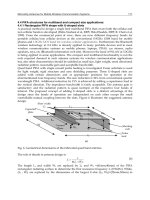
The Doherty PA employs multiple amplifiers, each contributing amplification for only a
subset of the power rage and is used to boost both the power added efficiency (PAE) at low
power and the 1-dB compression power (P
1dB
) and saturation power (P
sat
). The Doherty
amplifier shown in Fig. 9 employs two amplifier cells, the main amplifier cell and the
auxiliary amplifier cell. A transmission line network is used to split the input signal into two
amplifiers and comprises a quarter wavelength transmission line connecting the input to the
main amplifier cell with characteristic impedance of Z
0
= 50Ω, and a quarter wavelength
transmission line with characteristic impedance of Z
0
=
250
Ω connecting the inputs of
the main amplifier cell with the auxiliary amplifier cell. An identical transmission line
network is used to combine the outputs of the two amplifiers, with the output transmission
line connection used to compensate for the phase shift of the splitter. Both the input and
output networks are matched to 50Ω impedance.
The size of the transistors used in each main/auxiliary amplifier need to be carefully
investigated. Each transistor device needs to be carefully laid out to minimise parasitic
capacitance and substrate resistance. In this design each amplifier consists of five cascode
stages. The cascode unit building block was used in order to increase gain of the PA by
reducing the Miller capacitance, and also to improve the amplifiers stability. When biased at
200μA/μm each cascode stage possesses a maximum available gain (MAG) of 7dB at
60GHz. Micro-strip waveguides were used for impedance matching, interconnects and for
biasing of each amplifying stage. These cascode stages are AC coupled to allow independent
basing of the transistors for optimum operating conditions.
Fig. 10. Microphotograph of the 60-GHz Doherty power amplifier. The size of the PA
including testing pads is 1410μm by 1310μm.
The power amplifier is fabricated on the IBM 130-nm CMOS technology and its
microphotograph is shown in Fig. 10. The measured S-parameters shown in Fig. 11 reveal a
peak power gain, S
21
, of 15dB and a 3-dB bandwidth of 6GHz from 56.5GHz to 62.5GHz. The
input and output return losses, S
11
and S
22
, are less than -10dB for the entire frequency band
of interest from 57 to 66GHz. The output 1-dB compression power, P1dB, which can be
derived from the high-power performance of the PA shown in Fig. 12, is 7dBm. Fig. 13
shows the current consumption in the main and auxiliary amplifier at different input power
levels. The power added efficiency (PAE) of the PA is maximized when both the main and
auxiliary amplifiers are equally powered. The maximum PAE for this PA is 3%.
Fig. 11. Measured small-signal performance of the 60-GHz Doherty power amplifier
Fig. 12. Measured output power and gain of the 60-GHz Doherty power amplifier
MobileandWirelessCommunications:Networklayerandcircuitleveldesign292
Fig. 13. Measured current consumption and power added efficiency of the Doherty PA
The International Technology Roadmap for Semiconductors (ITRS, 2007) has defined an
FoM for the PA which links the output power (P
1dB
) with the gain, PAE, and frequency as a
standard to compare different PAs. Table 2 provides a comparison of this PA with other
published CMOS millimeter-wave PAs in terms of this FoM.
Reference
CMOS
tech.
Freq.
(GHz)
Gain
(dB)
P
sat
(dBm)
P
1dB
(dBm)
PAE
(%)
Architecture FoM
(Yao et al.
2007)
90-nm 60 5.2 9.3 6.4 7.4
3-stage
cascode
7.5
(Suzuki et al.
2008)
90-nm 60 8.0 10.6 8.2 -
3-stage
common source
-
90-nm 77 9.0 6.3 4.7 - -
(Chowdhury
et al. 2008)
90-nm 60 5.6 12.3 9.0 8.8
3-stage
transformer
19.5
(Wicks et al.
2008)
130-nm 77 6.0 8.1 6.3 0.5
5-stage
cascode
2.1
This work 130-nm 60 13.5 7.8 7.0 3.0 Doherty 15.2
Table 2. Performance comparison of the PA in this work and published millimetre-wave
PAs on CMOS technology
6. Mixer
The down-conversion mixer in the receiver is used to translate the input signal from RF to
an intermediate frequency (IF) for processing by baseband circuits. An important
consideration in homodyne receiver structures is the LO-to-RF isolation of the mixer. LO
self-mixing (Lee, 2004), occurs when the LO signal (which is at the same frequency as the RF
signal) leaks to the input of the mixer and then mixes with itself, produces a time varying
DC offset which significantly degrades the receiver’s performance especially in OFDM
systems. In the literature, few results have been presented for CMOS mixers which are
WirelessCommunicationsat60GHz:ASingle-ChipSolutiononCMOSTechnology 293
Fig. 13. Measured current consumption and power added efficiency of the Doherty PA
The International Technology Roadmap for Semiconductors (ITRS, 2007) has defined an
FoM for the PA which links the output power (P
1dB
) with the gain, PAE, and frequency as a
standard to compare different PAs. Table 2 provides a comparison of this PA with other
published CMOS millimeter-wave PAs in terms of this FoM.
Reference
CMOS
tech.
Freq.
(GHz)
Gain
(dB)
P
sat
(dBm)
P
1dB
(dBm)
PAE
(%)
Architecture FoM
(Yao et al.
2007)
90-nm 60 5.2 9.3 6.4 7.4
3-stage
cascode
7.5
(Suzuki et al.
2008)
90-nm 60 8.0 10.6 8.2 -
3-stage
common source
-
90-nm 77 9.0 6.3 4.7 - -
(Chowdhury
et al. 2008)
90-nm 60 5.6 12.3 9.0 8.8
3-stage
transformer
19.5
(Wicks et al.
2008)
130-nm 77 6.0 8.1 6.3 0.5
5-stage
cascode
2.1
This work 130-nm 60 13.5 7.8 7.0 3.0 Doherty 15.2
Table 2. Performance comparison of the PA in this work and published millimetre-wave
PAs on CMOS technology
6. Mixer
The down-conversion mixer in the receiver is used to translate the input signal from RF to
an intermediate frequency (IF) for processing by baseband circuits. An important
consideration in homodyne receiver structures is the LO-to-RF isolation of the mixer. LO
self-mixing (Lee, 2004), occurs when the LO signal (which is at the same frequency as the RF
signal) leaks to the input of the mixer and then mixes with itself, produces a time varying
DC offset which significantly degrades the receiver’s performance especially in OFDM
systems. In the literature, few results have been presented for CMOS mixers which are
suitable for homodyne architectures operating at the 60-GHz band (Emami et al., 2005). In
this section we describe the design of a 60-GHz double balanced Gilbert cell mixer with high
LO-to-RF isolation on CMOS technology.
Fig. 14. Double-balanced Gilbert cell mixer
Fig. 14 shows the schematic of the double-balanced mixer where biasing circuits have been
omitted for clarity. TL
2
and TL
4
are two microstrip lines serving as source degeneration
inductors and TL
1
and TL
3
are used to match the RF input to 50 Ω. The input impedance
looking into the transconductance stage formed by M
1
and M
2
can be shown to be equal to
1221
2
2
11
TLTLT
gs
TLTL
gs
TLm
gs
TLin
LjL
Cj
LjLj
C
Lg
Cj
LjZ
.
(1)
The expression above shows that by adjusting TL
1,2
we can match the input impedance to
50Ω for all different sizes of M
1,2
. It also can be shown that the inductive degeneration
increases linearity without raising the noise (Terrovitis, 2002). More over, by choosing the
optimum number of fingers of M
1,2
, the minimum noise figure, NF
min
, can also be achieved
simultaneously with input port matched.
The loads used in this Gilbert cell mixer as shown in Fig. 14 are a pair of PFET transistors.
This type of load is chosen in order to achieve sufficient bandwidth and gain given the
limited voltage headroom available when using a 1.2 V power supply. To get a higher
output resistance for these transistors, non-minimum channel length has been used and the
PFETs are biased in the strong inversion region. However, in order to drive a fixed amount
of current, the longer the channel, the wider the width of a transistor is required, which may
result in a large size of these PFETs. Thus, a trade-off must be made when determining the
size of the PFETs. A source follower buffer, not shown in Fig. 14, is added to the output of
the mixer to isolate the mixer core circuit and subsequent stages.
MobileandWirelessCommunications:Networklayerandcircuitleveldesign294
Because of the short wavelength of 60 GHz special considerations must be given to make the
circuit as symmetrical as possible in layout to maintain balance and common mode rejection.
Transmission line crossings as well as difference in path lengths are avoided when possible
since these mismatches increase the imbalance and reduce the isolation between LO, RF, and
IF ports. In this design, microstrip lines were used to implement the degeneration
impedance, matching networks and critical interconnects that carry high-frequency signal.
Micro-strip lines on silicon are typically implemented using the top- layer metal as the
signal line, and the bottom-layer metal for the ground plane. The metal layers on which the
signal line and the ground plane must be carefully determine so that a simple layout of the
mixer can be attained without degrading the quality factor of the microstrip lines.
A 60-GHz double-balanced CMOS mixer with high LO-to-RF isolation was designed and
fabricated following the design method described above. A microphotograph of the mixer is
shown in Fig. 15. This mixer achieves a voltage conversion gain of better than 2dB, as shown
in Fig. 16, input-referred IP3 of −8dBm and LO-to-RF isolation of greater than 36dB, as
shown in Fig. 17, when driven with an LO input of 0dBm.
Fig. 15. Microphotograph of the 60-GHz double balance mixer on CMOS with on-chip
transformer baluns for testing purpose
Fig. 16. Conversion gain of the 60-GHz double balance mixer on CMOS
WirelessCommunicationsat60GHz:ASingle-ChipSolutiononCMOSTechnology 295
Because of the short wavelength of 60 GHz special considerations must be given to make the
circuit as symmetrical as possible in layout to maintain balance and common mode rejection.
Transmission line crossings as well as difference in path lengths are avoided when possible
since these mismatches increase the imbalance and reduce the isolation between LO, RF, and
IF ports. In this design, microstrip lines were used to implement the degeneration
impedance, matching networks and critical interconnects that carry high-frequency signal.
Micro-strip lines on silicon are typically implemented using the top- layer metal as the
signal line, and the bottom-layer metal for the ground plane. The metal layers on which the
signal line and the ground plane must be carefully determine so that a simple layout of the
mixer can be attained without degrading the quality factor of the microstrip lines.
A 60-GHz double-balanced CMOS mixer with high LO-to-RF isolation was designed and
fabricated following the design method described above. A microphotograph of the mixer is
shown in Fig. 15. This mixer achieves a voltage conversion gain of better than 2dB, as shown
in Fig. 16, input-referred IP3 of −8dBm and LO-to-RF isolation of greater than 36dB, as
shown in Fig. 17, when driven with an LO input of 0dBm.
Fig. 15. Microphotograph of the 60-GHz double balance mixer on CMOS with on-chip
transformer baluns for testing purpose
Fig. 16. Conversion gain of the 60-GHz double balance mixer on CMOS
Fig. 17. LO-to-RF isolation of the 60-GHz double balance mixer on CMOS
7. Voltage controlled oscillator
The output power, tuning range and phase noise of the voltage controlled oscillator (VCO)
significantly affect the performance of the transceiver. In VCO design the voltage controlled
frequency of operation is achieved via voltage dependant capacitance devices such as
varactors. In many cases the phase noise of these oscillators is limited by the ability to build
high-quality inductors and varactors which form the LC tank that determines the frequency
of the VCO. In this application the VCO is required to have: a tuning range of 9 GHz, a
phase noise less than -90 dBc/Hz at 1 MHz and a sufficient output power to drive the four
mixers as shown in Fig. 1. Such stringent requirements mandate a trade-off between tuning
range and phase noise during the design of the VCO.
In MOS technology a varactor can be implemented by shorting the source and the drain
terminals of a MOSFET together and applying a control voltage across its gate and
source/drain terminals. The bias voltage governs the charge distribution in the channel and
subsequently the capacitance the varactor. To achieve maximum possible tuning range with
acceptably low phase noise, carefully designed inversion mode MOS varactors are
employed. For this particular 130-nm CMOS technology, the length of the NMOS varactors
are set equal to 260nm in order to achieve a capacitance tuning ratio of 3. An important
consideration in VCO design is the gate leakage current of the varactor increases the VCO’s
phase noise and its parasitic capacitance reduces the oscillation frequency (Lee & Liu, 2007).
Three candidate architectures for high-frequency VCO are fundamental VCO, VCO with
frequency doubler, and push-push VCO. The fundamental architecture is not very efficient
in this application since it has narrow tuning range and also requires a wide band divider in
the phase locked loop (PLL) which can consume significant power and space. Architectures
based on frequency doubling or push-push topology are better choices because they can
achieve twice the tuning range of the fundamental architecture. Another advantage of these
architectures is that the varactors operate at a lower frequency and have a higher quality
factor which results in reduced phase noise. Among these two architectures, the frequency
doubling architecture requires additional circuits such as a doubler/multiplier and filters
which can consume considerable space and power. Additionally insufficiently filtered
harmonics generated by the doubler can modulate the desired output frequency of the VCO
and increase the phase noise. The push-push architecture combines frequency generation
and frequency doubling in one circuit. In the push-push oscillator the fundamental and odd
MobileandWirelessCommunications:Networklayerandcircuitleveldesign296
harmonics cancel and power is delivered to the load at even harmonics. The push-push
architecture is chosen for this application.
Fig. 18. Circuit diagram of the push-push voltage controlled oscillator
Fig. 19. Microphotograph of the push-push voltage controlled oscillator
The differential cross-coupled LC oscillator with push-push output is shown in Fig. 18. The
LC tanks composing the inductor, L
1,2
, and the varactors, VAR
1,2
, determines the frequency
of oscillation. Frequency dependent signals at the drain of M
1
(M
2
) is cross-coupled to the
gate of M
2
(M
1
) which creates a negative impedance -1/g
m
where g
m
is the transconductance
of M
1,2
. This negative impedance is sized to exceed the losses of the LC tank to ensure
sustained oscillation. Most of designs include a tail current source to set the bias current and
provide high impedance which rejects noise from the power supply. However, due to the
mixing effect caused by nonlinearity in M
1,2
, the low frequency noise of the tail current
source is up converted to the output frequency of the oscillator and degrades the phase
noise of the oscillator. In this design, the current source is omitted to suppress this
contribution to the phase noise. The circuit shown in Fig. 18 is implemented on standard
130nm CMOS technology. In this design the transistors M
1,2
have 50 fingers and total width
WirelessCommunicationsat60GHz:ASingle-ChipSolutiononCMOSTechnology 297
harmonics cancel and power is delivered to the load at even harmonics. The push-push
architecture is chosen for this application.
Fig. 18. Circuit diagram of the push-push voltage controlled oscillator
Fig. 19. Microphotograph of the push-push voltage controlled oscillator
The differential cross-coupled LC oscillator with push-push output is shown in Fig. 18. The
LC tanks composing the inductor, L
1,2
, and the varactors, VAR
1,2
, determines the frequency
of oscillation. Frequency dependent signals at the drain of M
1
(M
2
) is cross-coupled to the
gate of M
2
(M
1
) which creates a negative impedance -1/g
m
where g
m
is the transconductance
of M
1,2
. This negative impedance is sized to exceed the losses of the LC tank to ensure
sustained oscillation. Most of designs include a tail current source to set the bias current and
provide high impedance which rejects noise from the power supply. However, due to the
mixing effect caused by nonlinearity in M
1,2
, the low frequency noise of the tail current
source is up converted to the output frequency of the oscillator and degrades the phase
noise of the oscillator. In this design, the current source is omitted to suppress this
contribution to the phase noise. The circuit shown in Fig. 18 is implemented on standard
130nm CMOS technology. In this design the transistors M
1,2
have 50 fingers and total width
of 50μm. The NMOS varactors VAR
1,2
are implemented as a multi-finger structure to reduce
gate resistance and enhance the resonator’s quality factor. The inductors L
1,2
are fabricated
on the top metal layer to achieve the highest quality factor possible. These inductors are
realized as 100μm-long, 25μm-wide RF transmission lines and have an equivalent
inductance value of 50pH. A microphotograph of the VCO is shown in Fig. 19.
The fabricated VCO has an output frequency range of 65.8GHz to 73.6GHz as shown in Fig.
20. After calibrating the cable and pads loss, the output power at 70GHz is -4dBm. The core
power consumption is 32mW. The phase noise was measured by down converting the
VCO’s signal to an intermediate frequency of 2.5GHz. The measured phase noise is -92
dBc/Hz at 1 MHz offset (from a center frequency of 66GHz) and -107 dBc/Hz at 10 MHz
offset (from a center frequency of 66GHz). Frequency variation with temperature was also
measured from 0 to 70 degrees Celsius. The maximum frequency deviation is less than
200MHz in this temperature range as illustrated in Fig. 21.
Fig. 20. Output frequency versus control voltage of the VCO
Fig. 21. Frequency shift due to temperature variation
MobileandWirelessCommunications:Networklayerandcircuitleveldesign298
8. Biasing and control
The advancement of CMOS technology is driven by digital integrated circuits which operate
faster with transistors with shorter channel length and consume less power with lower
power supply voltage. These advantages of digital circuits are due to the fact that digital
circuits are less sensitive to temperature, voltage, and power (PVT) variation compared to
analog/RF circuits. Analog/RF circuits require special treatment during the design to
reduce their sensitive to PVT variation that is significant on CMOS integrated circuits. The
60-GHz transceiver chip designed in this work adopts an on-chip Digital Control Interface
(DCI) to digitally tune the behaviour of analog/RF components to remedy the performance
degradation due to PVT variation thereby increasing the overall yield of the transceiver.
Fig. 22. Block diagram of the digital control interface
The DCI architecture is shown in Fig. 22. It comprises a DCI master and a DCI slave
communicating with each other via a serial peripheral interface (SPI) bus and a bank of 6-bit
registers and 6-bit digital-to-analog converters (DACs) connected to the DCI slave. For a
two-chip radio solution, the DCI master resides on the digital/baseband chip while the DCI
slave, register bank, and DAC bank reside on the analog/RF chip.
A tuning algorithm implemented on the digital chip will determine when a certain biasing
voltage needs to be changed. The tuning algorithm will then send a request to the DCI
master indicating the address of the register and the new value of the register. The DCI
master passes these values to the DCI slave, via the SPI bus, which outputs the new value to
the required register. The corresponding DAC translates the value stored in the register to
the required analog voltage. The DCI slave can also receive feedback from analog/RF
circuits and transfer this to the digital chip to assist the tuning algorithm. Real-time
monitoring and tuning of the operation of the transceiver is therefore made possible with
the integrated DCI.
The layout of the DCI is shown in Fig. 23. In this design, the DCI master and DCI slave are
implemented together on the 60-GHz analog/RF chip.
WirelessCommunicationsat60GHz:ASingle-ChipSolutiononCMOSTechnology 299
8. Biasing and control
The advancement of CMOS technology is driven by digital integrated circuits which operate
faster with transistors with shorter channel length and consume less power with lower
power supply voltage. These advantages of digital circuits are due to the fact that digital
circuits are less sensitive to temperature, voltage, and power (PVT) variation compared to
analog/RF circuits. Analog/RF circuits require special treatment during the design to
reduce their sensitive to PVT variation that is significant on CMOS integrated circuits. The
60-GHz transceiver chip designed in this work adopts an on-chip Digital Control Interface
(DCI) to digitally tune the behaviour of analog/RF components to remedy the performance
degradation due to PVT variation thereby increasing the overall yield of the transceiver.
Fig. 22. Block diagram of the digital control interface
The DCI architecture is shown in Fig. 22. It comprises a DCI master and a DCI slave
communicating with each other via a serial peripheral interface (SPI) bus and a bank of 6-bit
registers and 6-bit digital-to-analog converters (DACs) connected to the DCI slave. For a
two-chip radio solution, the DCI master resides on the digital/baseband chip while the DCI
slave, register bank, and DAC bank reside on the analog/RF chip.
A tuning algorithm implemented on the digital chip will determine when a certain biasing
voltage needs to be changed. The tuning algorithm will then send a request to the DCI
master indicating the address of the register and the new value of the register. The DCI
master passes these values to the DCI slave, via the SPI bus, which outputs the new value to
the required register. The corresponding DAC translates the value stored in the register to
the required analog voltage. The DCI slave can also receive feedback from analog/RF
circuits and transfer this to the digital chip to assist the tuning algorithm. Real-time
monitoring and tuning of the operation of the transceiver is therefore made possible with
the integrated DCI.
The layout of the DCI is shown in Fig. 23. In this design, the DCI master and DCI slave are
implemented together on the 60-GHz analog/RF chip.
Fig. 23. Layout of the digital control interface
9. 60-GHz single-chip transceiver on CMOS
A 60-GHz single-chip CMOS transceiver was realized by integrating the circuits described
above on a single silicon substrate. A microphotograph of the designed chip is shown in Fig.
24. The die measures 5mm by 5mm. Prior to this work, 60-GHz transmitters and receivers
have been implemented on CMOS (Razavi, 2006; Emami et al., 2007) as well as BiCMOS
(Reynolds et al., 2006). However, none of them achieved a high level of integration like this
design where the transmitter and the receiver, the analog/RF circuits, the digital circuits,
and the RF passive filters are all included in a single chip.
PLL
Receiver
Transmitter
Digital control
interface
Fig. 24. The 60-GHz single-chip transceiver on 130-nm CMOS technology
The on-chip 60-GHz PLL subsystem was found not function properly even though the
functionality and performance of the most challenging circuit, the 60-GHz VCO, had been
MobileandWirelessCommunications:Networklayerandcircuitleveldesign300
verified with measurement results as described in Section 7. An external LO signal was
utilized for the purpose of demonstrating the operation of the transmitter and the receiver.
The DCI functionality is satisfactory. In all measurement described below, a computer is
utilized to control the DCI master. The biasing voltages for the transceiver are set by sending
instructions from the computer to the DCI master via an FPGA board.
(a)
(b)
Fig. 25. Measured output power of the 60-GHz transmitter: (a) saturated output power at
different output frequencies, and (b) output power versus input power at 60 GHz
The transmitter consumes a total DC power of 515mW. The transmitting capability of the
transmitter is presented in Fig. 25. Fig. 25 (a) shows the saturated output power, P
sat
, of the
transmitter at different frequencies in the 56 to 64GHz band. The output power is at its peak
of 6.5dBm for frequencies from 58 to 60GHz. At the high end of the spectrum, the output
power is reduced to approximately 2dBm due to the degraded performance of the
constituent circuits at high frequency. The output 1-dB compression power was also
measured and the collected data is plotted in Fig. 25 (b). At 60 GHz, the output P
1dB
is
1.6dBm.
The performance of the receiver including its conversion gain and linearity was measured
by on-wafer probing. Noise figure measurement was not carried out due to the lack of
WirelessCommunicationsat60GHz:ASingle-ChipSolutiononCMOSTechnology 301
verified with measurement results as described in Section 7. An external LO signal was
utilized for the purpose of demonstrating the operation of the transmitter and the receiver.
The DCI functionality is satisfactory. In all measurement described below, a computer is
utilized to control the DCI master. The biasing voltages for the transceiver are set by sending
instructions from the computer to the DCI master via an FPGA board.
(a)
(b)
Fig. 25. Measured output power of the 60-GHz transmitter: (a) saturated output power at
different output frequencies, and (b) output power versus input power at 60 GHz
The transmitter consumes a total DC power of 515mW. The transmitting capability of the
transmitter is presented in Fig. 25. Fig. 25 (a) shows the saturated output power, P
sat
, of the
transmitter at different frequencies in the 56 to 64GHz band. The output power is at its peak
of 6.5dBm for frequencies from 58 to 60GHz. At the high end of the spectrum, the output
power is reduced to approximately 2dBm due to the degraded performance of the
constituent circuits at high frequency. The output 1-dB compression power was also
measured and the collected data is plotted in Fig. 25 (b). At 60 GHz, the output P
1dB
is
1.6dBm.
The performance of the receiver including its conversion gain and linearity was measured
by on-wafer probing. Noise figure measurement was not carried out due to the lack of
appropriate noise sources. The noise figure of the receiver computed from the noise figures
and gains of its building blocks is 11.7dB. The receiver consumes a total power of 54mW.
The conversion gain of the receiver is presented in Fig. 26 (a) as functions of the IF
frequency. A maximum conversion gain of 8.1 dB is achieved with f
LO
=58GHz and
f
IF
=200MHz. The conversion gain of the receiver is reduced at high LO frequencies because
of the reduced gain of the LNA and the down-conversion mixers at high frequencies.
(a)
(b)
Fig. 26. Measured (a) conversion gain and (b) IIP
3
of the 60-GHz receiver
The linearity of the receiver, quantified by its IIP
3
, was estimated from a two-tone test. Two
Anritsu MG3690B signal generators were used to generate the two testing tones for the
measurement. Due to the lack of another high power 60-GHz signal generator, the LO
power was not set up properly for optimum performance of the receiver. Thus the
conversion gain of the receiver was reduced substantially in this measurement. It is assumed
that the output power of the fundamental tone and the third-order inter-modulation tone
were reduced by the same factor so that the IIP
3
computed for the non-optimum operation
MobileandWirelessCommunications:Networklayerandcircuitleveldesign302
conditions closely tracks the IIP
3
of the receiver in its optimum operation conditions. The
measured data is plotted in Fig. 26 (b). The IIP
3
of the receiver is approximately -13.74dBm.
10. Conclusion and future work
Recent advances in millimeter-wave electronics have made it possible for a complete
wireless transceiver-on-a-chip system to be realized. In order to achieve a low-cost and high-
integration solution CMOS is the process of choice. In this chapter we have shown the
feasibility of implementing a wireless transceiver on a single chip operating in the
millimeter-wave band on CMOS. The 60-GHz CMOS transceiver comprises a transmitter, a
receiver, a phase-locked loop, and a digital control interface, and was implemented for the
first time on a single silicon die.
The demonstration of the 60-GHz transceiver on a 130-nm CMOS process in this research,
even without a working on-chip PLL, has proved the capability of CMOS technology in
millimeter-wave circuit domain. However, there is still a large gap, technically and
economically, that must be bridged before a truly low-cost, low-power, multi-Gbps CMOS
transceiver IC can be achieved. The rest of this section discusses some future work in the
process of realization such an IC.
All the circuits in this work was developed on a 130-nm CMOS technology since this was
the most advanced CMOS technology characterized up to millimeter-wave frequencies at
the time the research started. Owing to the fast scaling speed of CMOS technology, more
advanced CMOS processes have been recently put into production by different foundries
around the world. Moving the design to a more advanced technology, for example, a 65-nm
CMOS technology, promises a better performance of the transceiver.
A directional, steerable phased-array antenna system is an attractive solution to overcome
the high path loss at millimeter-wave frequencies and to enable transmission in non-line-of-
sight conditions. The configuration of the array, i.e. one or two dimensional array, and the
number of the elemental antennae, however, must be carefully determined to achieve the
required link budget under certain form factor, cost, and power consumption constraints.
Since the antenna is implemented off-chip, the interface between the antenna and the CMOS
transceiver across the chip boundary must be carefully studied. The interconnect between
the antenna and the input/output pad on the CMOS chip, whether it is wire-bond or solder
bump, must be taken into account during the design of the antenna. Further research must
be carried out to understand the characteristic of these interconnects at millimeter-wave
frequencies to facilitate the antenna design.
Acknowledgment
The authors would like to thank MOSIS, IBM, Cadence, Anritsu, and SUSS MicroTec for
their support. This research is funded by National ICT Australia (NICTA). NICTA is funded
by the Australian Government as represented by the Department of Broadband,
Communications and the Digital Economy and the Australian Research Council through the
ICT Centre of Excellence program.
WirelessCommunicationsat60GHz:ASingle-ChipSolutiononCMOSTechnology 303
conditions closely tracks the IIP
3
of the receiver in its optimum operation conditions. The
measured data is plotted in Fig. 26 (b). The IIP
3
of the receiver is approximately -13.74dBm.
10. Conclusion and future work
Recent advances in millimeter-wave electronics have made it possible for a complete
wireless transceiver-on-a-chip system to be realized. In order to achieve a low-cost and high-
integration solution CMOS is the process of choice. In this chapter we have shown the
feasibility of implementing a wireless transceiver on a single chip operating in the
millimeter-wave band on CMOS. The 60-GHz CMOS transceiver comprises a transmitter, a
receiver, a phase-locked loop, and a digital control interface, and was implemented for the
first time on a single silicon die.
The demonstration of the 60-GHz transceiver on a 130-nm CMOS process in this research,
even without a working on-chip PLL, has proved the capability of CMOS technology in
millimeter-wave circuit domain. However, there is still a large gap, technically and
economically, that must be bridged before a truly low-cost, low-power, multi-Gbps CMOS
transceiver IC can be achieved. The rest of this section discusses some future work in the
process of realization such an IC.
All the circuits in this work was developed on a 130-nm CMOS technology since this was
the most advanced CMOS technology characterized up to millimeter-wave frequencies at
the time the research started. Owing to the fast scaling speed of CMOS technology, more
advanced CMOS processes have been recently put into production by different foundries
around the world. Moving the design to a more advanced technology, for example, a 65-nm
CMOS technology, promises a better performance of the transceiver.
A directional, steerable phased-array antenna system is an attractive solution to overcome
the high path loss at millimeter-wave frequencies and to enable transmission in non-line-of-
sight conditions. The configuration of the array, i.e. one or two dimensional array, and the
number of the elemental antennae, however, must be carefully determined to achieve the
required link budget under certain form factor, cost, and power consumption constraints.
Since the antenna is implemented off-chip, the interface between the antenna and the CMOS
transceiver across the chip boundary must be carefully studied. The interconnect between
the antenna and the input/output pad on the CMOS chip, whether it is wire-bond or solder
bump, must be taken into account during the design of the antenna. Further research must
be carried out to understand the characteristic of these interconnects at millimeter-wave
frequencies to facilitate the antenna design.
Acknowledgment
The authors would like to thank MOSIS, IBM, Cadence, Anritsu, and SUSS MicroTec for
their support. This research is funded by National ICT Australia (NICTA). NICTA is funded
by the Australian Government as represented by the Department of Broadband,
Communications and the Digital Economy and the Australian Research Council through the
ICT Centre of Excellence program.
11. References
Abidi, A. (1995). Direct-conversion radio transceivers for digital communications, IEEE
Journal of Solid-State Circuits, Vol. 30, No. 12, pp. 1399-1410, ISSN 0018-9200
Chowdhury, D.; Reynaert, P. & Niknejad, A. M. (2008). A 60GHz 1V +12.3dBm
Transformer-Coupled Wideband PA in 90nm CMOS, Digest of Technical Papers of the
2008 IEEE International Solid-State Circuits Conference, ISBN 978-1-4244-2010-0, pp.
560-561, Feb. 2008, S
3
Digital Publishing Inc., Lisbon Falls, Maine, USA
Cohen, E.; Ravid, S. & Ritter, D. (2008). An ultra low power LNA with 15dB gain and 4.4dB
NF in 90nm CMOS process for 60 GHz phase array radio, Proceedings of the 2008
IEEE Radio Frequency Integrated Circuits Symposium, ISBN 978-1-4244-1809-1, pp. 61-
64, Atlanta, Georgia, USA, June 2008, IEEE, Piscataway
Doan, C. H.; Emami, S.; Niknejad, A. M. & Brodersen, R. W. (2005). Millimeter-Wave CMOS
Design, IEEE Journal of Solid-State Circuits, Vol. 40, No. 1, Jan. 2005, pp. 144-155,
ISSN 0018-9200
Emami, S.; Doan, C. H., Niknejad, A. M. & Brodersen, R. W. (2005). A 60-GHz down-
converting CMOS single-gate mixer, Digest of Papers of the 2005 IEEE Radio
Frequency Integrated Circuits Symposium, pp. 163-166, ISBN 0-7803-8983-2, Long
Beach, California, USA, June 2005, IEEE, Piscataway
Emami, S.; Doan, C. H.; Niknejad, A. M. & Brodersen, R. W. (2007). A Highly Integrated
60GHz CMOS Front-End Receiver, Digest of Technical Papers of the 2007 IEEE
International Solid-State Circuits Conference, pp. 190-191, ISBN 1-4244-0853-9, San
Francisco, California, USA, Feb. 2007, IEEE, Piscataway
Guo, N.; Qiu, R. C.; Mo, S. S. & Takahashi, K. (2007). 60-GHz millimeter-wave radio:
Principle, technology, and new results, EURASIP Journal on Wireless
Communications and Networking, Vol. 2007, Article ID 68253, 8 pages, ISSN 1687-1472
Heydari, B.; Bohsali, M.; Adabi, E. & Niknejad, A. M. (2007). Low-power mm-wave
components up to 104GHz in 90nm CMOS, Digest of Technical Papers of the 2007
IEEE International Solid-State Circuits Conference, ISBN 1-4244-0853-9, pp. 200–597,
San Francisco, California, USA, Feb. 2007, IEEE, Piscataway
ITRS (2007). International technology roadmap for semiconductors. />
Lee, T. H. (2004). The Design of CMOS Radio-Frequency Integrated Circuit, 2nd Edition,
Cambridge University Press, ISBN 0-521-83539-9, Cambridge, United Kingdom
Lee, C. & Liu, S L. (2007). A 58-to-60.4GHz Frequency Synthesizer in 90nm CMOS, Digest of
Technical Papers of the 2007 IEEE International Solid-State Circuits Conference, ISBN 1-
4244-0852-0, pp. 196-596, San Francisco, California, USA, Feb. 2007, IEEE,
Piscataway
Lee, S Y. & Tsai, C M. (2000). New Corss-Coupled Filter Design Using Improved Hairpin
Resonators, IEEE Transactions on Microwave Theory and Techniques, Vol. 48, No. 12,
Dec. 2000, pp. 2482-2490, ISSN 0018-9480
Lo, C M.; Lin, C S. & Wang, H. (2006). A miniature V-band 3-stage cascode LNA in 0.13μm
CMOS, Digest of Technical Papers of the 2006 IEEE International Solid-State Circuits
Conference, ISBN 1-4244-0079-1, pp. 1254–1263, San Francisco, California, USA, Feb.
2006, S
3
Digital Publishing Inc., Lisbon Falls, Maine, USA
Natarajan, A.; Nicolson, S.; Tsai, M D. & Floyd, B. (2008). A 60GHz variable-gain LNA in
65nm CMOS, Proceedings of the 2008 IEEE Asian Solid-State Circuits Conference, pp.
117-120, ISBN 978-1-4244-2605-8, Fukuoka, Japan, Nov. 2008, IEEE, Piscataway
MobileandWirelessCommunications:Networklayerandcircuitleveldesign304
Razavi, B. (2006). CMOS transceivers for the 60-GHz band, Digest of Technical Papers of the
2006 IEEE Radio Frequency Integrated Circuits Symposium, 4 pages, ISBN 0-7803-9572-
7, San Francisco, California, USA, June 2006, IEEE, Piscataway
Reynolds, S. K.; Floyd, B. A.; Pfeiffer, U. R.; Beukema, T.; Grzyb, J.; Haymes, C.; Gaucher, B.
& Soyuer, M. (2006). A Silicon 60-GHz Receiver and Transmitter Chipset for
Broadband Communications, IEEE Journal of Solid-State Circuits, Vol. 41, No. 12, pp.
2820-2831, ISSN 0018-9200
Suzuki, T.; Kawano, Y.; Sato, M.; Hirose, T. & Joshin, K. (2008). 60 and 77GHz Power
Amplifiers in Standard 90nm CMOS, Digest of Technical Papers of the 2008 IEEE
International Solid-State Circuits Conference, ISBN 978-1-4244-2010-0, pp. 562-563, San
Francisco, California, USA, Feb. 2008, S
3
Digital Publishing Inc., Lisbon Falls,
Maine, USA
Terrovitis, E. (2001). Analysis and Design of Current-Commutating CMOS Mixers. PhD
dissertation, EECS Department, University of California, Berkeley
Wicks, B.; Skafidas, E.; Evans, R. J. & Mareels, I. M. (2007). A 46.7-46.9 GHz CMOS MMIC
Power Amplifier for Automotive Applications, Proceedings of the Fourth IASTED
International Conference on Antennas, Radar and Wave Propagation, ISBN 978-0-88986-
661-4, pp. 80-84, Montreal, Quebec, Canada, May-June 2007, ACTA Press,
Anaheim, California, USA
Wicks, B. N.; Skafidas, E.; Evans, R. J. & Mareels, I. (2008). A 75–95 GHz Wideband CMOS
Power Amplifier, Proceedings of the 2008 European Microwave Integrated Circuits
Conference, ISBN 978-2-87487-007-1, pp. 554-557, Amsterdam, The Netherlands, Oct.
2008
Yang, B.; Skafidas, E. & Evans, R. J. (2008). Design of 60 GHz Millimetre-wave Bandpass
Filter on Bulk CMOS, IET Microwaves, Antennas & Propagation, ISSN 1751-8725
(accepted for publication)
Yao, T.; Gordon, M.; Yau, K.; Yang, M. T. & Voinigescu, S. P. (2006). 60-GHz PA and LNA in
90-nm RF-CMOS, Digest of Papers of the 2006 IEEE Radio Frequency Integrated Circuits
Symposium, 4 pages, ISBN 0-7803-9572-7, San Francisco, California, USA, June 2006,
IEEE, Piscataway
CurrentTrendsofCMOSIntegratedReceiverDesign 305
CurrentTrendsofCMOSIntegratedReceiverDesign
C.E.CapovillaandL.C.Kretly
X
Current Trends of CMOS Integrated
Receiver Design
C. E. Capovilla and L. C. Kretly
School of Electrical and Computer Engineering, University of Campinas
Campinas, São Paulo, Brazil
1. Introduction
The use of CMOS technology for implementation of fully RFICs (Radio Frequency
Integrated Circuits) is shown as a trend in the new devices for wireless communications.
Nowadays, these circuits are found in many kind of applications, in which they can provide
a lot of services including: Cellular Phones, Personal Mobile Service, Satellite, Specialized
Radios (used by the Police, Fire-fighters, Emergency Services), and WLANs (Wireless Local
Area Networks).
The potential of CMOS RFIC has been demonstrated in many academic works and by
commercial devices. Due to the quick development of 3G and 4G technologies and the
design of devices for systems that operate at standards such as WCDMA (Wideband Code
Division Multiple Access), GSM/GPRS (Global System for Mobile Communication/General
Packet Radio Service), WiMAX (Worldwide Interoperability for Microwave Access), and
WiBro (Wireless Broadband), the CMOS RFIC has been more and more inserted, because of
its good technical and commercial characteristics, becoming itself a challenge for the
designers (Iniewski, 2007).
For modern and appropriated RFIC applications, new mobile systems demand antennas in
small dimensions with wideband and reasonable gain, offering the possibility of a
multiband operation (Liberti & Rappaport, 1999).
In addition, the UWB (Ultra WideBand) communication systems are an important
advancement in wireless applications. They use a wide range of frequencies at very low
power to transmit at high data rate. The low power allows these systems to use existing
licensed RF bands without interfering with current users (Ismail & Gonzalez, 2006).
With the coming of the new digital standards, the data exchange over the wireless became
predominant. In fact, in the 1990s, the GSM and IS-95 standards, evolved to include data
transmission as an effective part of its services. Besides, the 3G and 4G are being applied
and developed with voice and data integration. It has been foreseen that the data traffic will
overtake the voice one. Furthermore, nowadays the costs of these devices and services for
the data traffic are cheap enough to permit its continuous utilization into user's houses and
offices.
In this way, the aim of this chapter is to provide a guide to the RF building blocks of smart
communication receivers in accordance with the present state of the art. The goal is to show
15
MobileandWirelessCommunications:Networklayerandcircuitleveldesign306
the conception and development of several RFICs, for example, LNAs (Low Noise
Amplifiers), mixer, and VCOs (Voltage Controlled Oscillators) in different applications.
The circuits presented here can supply the necessities for many mobile applications, in
particular, for SMILE (Spatial MultIplexing of Local Elements) front-end receiver circuitry.
As an example of a circuit developed for this technique, it is shown a multiplexed LNA with
four channels to supply the necessity of multiplexing without losing the concern about noise
or any other kind of design performance parameters (Capovilla et al., 2007). Page constraints
have made it necessary to limit coverage in some areas to represents different areas as best
as possible.
2. Smart receivers
The antenna array is one of the most promising techniques for increasing the system
capacity in wireless communication. The demand for mobile systems emerges and the use of
data transmission grows through applications of several protocols.
With the quick development of 3G and 4G technologies and the growth of the commercial
applications for their equipments, the seeking for antenna technical solutions has increased
a lot for these applications. Due to this fact, the antennas represent a fundamental role in its
performance, strengthening this research area.
Using a variety of processing algorithms, usually managed by a DSP (Digital Signal
Processor), the adaptive antennas adjust its radiation pattern dynamically to enhance the
desired signal, null or reduce interference (Liberti & Rappaport, 1999). They are used to
improve the received signals, minimizing interference and maximizing the desired receiving
signal and to form dynamic beams.
Fig. 1. – Adaptive array concept.
An adaptive system considers that the desired signal and the interfering one come from
different directions. As can be seen in Fig. 1, to reduce the fading and the co-channel
CurrentTrendsofCMOSIntegratedReceiverDesign 307
the conception and development of several RFICs, for example, LNAs (Low Noise
Amplifiers), mixer, and VCOs (Voltage Controlled Oscillators) in different applications.
The circuits presented here can supply the necessities for many mobile applications, in
particular, for SMILE (Spatial MultIplexing of Local Elements) front-end receiver circuitry.
As an example of a circuit developed for this technique, it is shown a multiplexed LNA with
four channels to supply the necessity of multiplexing without losing the concern about noise
or any other kind of design performance parameters (Capovilla et al., 2007). Page constraints
have made it necessary to limit coverage in some areas to represents different areas as best
as possible.
2. Smart receivers
The antenna array is one of the most promising techniques for increasing the system
capacity in wireless communication. The demand for mobile systems emerges and the use of
data transmission grows through applications of several protocols.
With the quick development of 3G and 4G technologies and the growth of the commercial
applications for their equipments, the seeking for antenna technical solutions has increased
a lot for these applications. Due to this fact, the antennas represent a fundamental role in its
performance, strengthening this research area.
Using a variety of processing algorithms, usually managed by a DSP (Digital Signal
Processor), the adaptive antennas adjust its radiation pattern dynamically to enhance the
desired signal, null or reduce interference (Liberti & Rappaport, 1999). They are used to
improve the received signals, minimizing interference and maximizing the desired receiving
signal and to form dynamic beams.
Fig. 1. – Adaptive array concept.
An adaptive system considers that the desired signal and the interfering one come from
different directions. As can be seen in Fig. 1, to reduce the fading and the co-channel
interference, the system processes four input signals coming from different antennas of the
array (u1(t), u2(t), u3(t), and u4(t)) to generate an output optimized signal.
This one is the work of the crossed correlation and of the relative signal levels between four
received signals. The radiation pattern can be configured in real time through direct
application of control algorithms as MUSIC (Multiple Signal Classification) (Ratnarajah &
Manikas, 1998) and ESPRIT (Estimation of Signal Parameters via Rotational Invariance
Techniques) (Roy & Kailath, 1989), which are examples of DOA (Direction Of Arrival)
algorithms.
To estimate the best weight of the array (Godara, 1997a), efficient algorithms as LMS (Least
Mean Squares) (Clarkson & White, 1987) and RLS (Recursive Least Squares) (Qiao, 1991) can
be used. Due to this control over the radiation pattern envisaging a better management of
the system, it is also possible to form dynamic cells using the multiple beams. This
technique is known as SDMA (Space Division Multiple Access) (Godara, 1997b), and allows
for different users the simultaneous operation of the same time/frequency slot, increasing
the capacity of the system (Kuehner et al., 2001).
Fig. 2. – SMILE RF front-end receiver architecture.
Additionally, there are several techniques for optimization of smart antennas in spatial
diversity. The DBF (Digital BeamForming) is one of those techniques that revolutionized the
capabilities of antenna arrays. In the beginning, the DBF projects were motivated by military
operations, however with the increasing interest in low cost WLAN, nowadays, there are
studies in order to use the DBF in different applications. The DBF scheme provides a lot of
advantages over analog beamforming including in hardware implementation (Doble &
Litva, 1996).
For this one, the smart antenna array requires independent RF channels (RF switch, LNA,
and mixer) for each array element, increasing hardware costs and the power consumption,
which are proportional to the number of array elements. In this way, many efforts have been
made aiming at reducing the use of repetitive RF channels. The works of Cheng (2001) and
Ishii (2000) show some of the attempts in this direction, but only for limited functional
environmental conditions.
MobileandWirelessCommunications:Networklayerandcircuitleveldesign308
The SMILE scheme is shown in Fig. 2. It appears as a new solution to solve these technical
problems. This hardware technique reduces the RF channels of the smart receiver to only
one without loss of signal fidelity. This functional characteristic is obtained by
independently switching the array elements at a rate above the Nyquist frequency,
according to the sampling theory. After processing the RF channel (through RF switch,
LNA, and mixer), the spatially sampled signals are demultiplexed and low-pass filtered to
form only one output (Fredrick et al., 2002).
Fig. 3. – Baseband SMILE spectrum.
To test the scheme, a single-tone test was performed with an IF of 750kHz. After receiving
the signal, the baseband spectrum of the multiplexed signal for the array rotate at 45º is
shown in Fig. 3. Each of the four channels demultiplexed and recovered are shown in Fig. 4.
The envelope shows the original data samples. This technique significantly reduces the RF
hardware, getting the necessary functionality with only a fraction of the hardware
requirements. Compared to N elements from a traditional system, the proposed system
offers an N fold reduction in the RF hardware requirement also reducing the power
consumption and the circuit size.
3. CMOS receivers
The RF basic blocks of receivers are composed by LNA, mixer, and LO (Local Oscillator). In
this section, these circuits are presented and characterized in CMOS technology. Normally,
at the foundry, the CMOS RF technology is derived from a process for manufacturing digital
circuits, after a stabilization procedure, by adding masks and performing other slight
modifications, such as, the use of thick metal technique for the top layer (Backer et al., 2001).
CurrentTrendsofCMOSIntegratedReceiverDesign 309
The SMILE scheme is shown in Fig. 2. It appears as a new solution to solve these technical
problems. This hardware technique reduces the RF channels of the smart receiver to only
one without loss of signal fidelity. This functional characteristic is obtained by
independently switching the array elements at a rate above the Nyquist frequency,
according to the sampling theory. After processing the RF channel (through RF switch,
LNA, and mixer), the spatially sampled signals are demultiplexed and low-pass filtered to
form only one output (Fredrick et al., 2002).
Fig. 3. – Baseband SMILE spectrum.
To test the scheme, a single-tone test was performed with an IF of 750kHz. After receiving
the signal, the baseband spectrum of the multiplexed signal for the array rotate at 45º is
shown in Fig. 3. Each of the four channels demultiplexed and recovered are shown in Fig. 4.
The envelope shows the original data samples. This technique significantly reduces the RF
hardware, getting the necessary functionality with only a fraction of the hardware
requirements. Compared to N elements from a traditional system, the proposed system
offers an N fold reduction in the RF hardware requirement also reducing the power
consumption and the circuit size.
3. CMOS receivers
The RF basic blocks of receivers are composed by LNA, mixer, and LO (Local Oscillator). In
this section, these circuits are presented and characterized in CMOS technology. Normally,
at the foundry, the CMOS RF technology is derived from a process for manufacturing digital
circuits, after a stabilization procedure, by adding masks and performing other slight
modifications, such as, the use of thick metal technique for the top layer (Backer et al., 2001).
Fig. 4. – Recovered multichannel baseband data for array at 45º.
3.1 Low noise amplifier
The schematic of a basic common-source LNA is shown in Fig. 5. For simplicity, the bias
network is represented only by Vbias and Rb (usually 5-10k). The input and output are
coupled with DC-block capacitors (not showed here). The use of inductive degeneration
results in no additional noise generation since the real part of the input impedance does not
correspond to a physical resistor. A mathematical representation of the noise from the whole
amplifier circuit with neglected noise contribution of the transistor Mn2, is given by (Allstot
et al.,2004):
)(1
5
21
5
1
1
1
2
2
2
0
γ
δα
cQ
γ
δα
ω
ω
Qα
γ
F
T
with:
5 6 7 8 9 10 11 12
-0,4
-0,3
-0,2
-0,1
0,0
0,1
0,2
0,3
0,4
Amplitude (V)
Time (s)
5 6 7 8 9 10 11 12
-0,4
-0,3
-0,2
-0,1
0,0
0,1
0,2
0,3
0,4
Amplitude (V)
Time (s)
5 6 7 8 9 10 11 12
-0,4
-0,3
-0,2
-0,1
0,0
0,1
0,2
0,3
0,4
Amplitude (V)
Time (s)
5 6 7 8 9 10 11 12
-0.4
-0.3
-0.2
-0.1
0.0
0.1
0.2
0.3
0.4
Amplitude (V)
Time (s)
0d
m
g
g
sgs
RC
Q
0
1
MobileandWirelessCommunications:Networklayerandcircuitleveldesign310
where: Q is the quality factor, g
d0
is the drain conductance, and, , , c are fixed transistor
parameters.
Fig. 5. – LNA schematic.
A simple analysis of the input impedance (Shaeffer & Lee, 2001) shows that:
)(2
1
gs
sm
gs
gsin
C
Lg
sC
LLsZ
where: L
s
and L
g
are source and gate inductors, respectively, and g
m
and C
gs
denote small
signal parameters of transistor Mn1 (C
gd
and C
ds
are neglected in this first-order
approximation).
The input is matched to 50 by using inductors L
g
and L
s
, with the source inductor L
s
chose
to match the real part, and gate inductor L
g
used to set the resonance frequency. Using some
assumptions taken from the long-channel theory, the optimum width of the device Mn1 is
given by (Lee, 1998):
)(3
3
1
0
1
soxeff
Mn
RCL
W
where: L
eff
is the effective transistor length and C
ox
is the oxide capacitance of the transistor.
Equation 3 gives a definite width of the transistor, but for short channel devices, the CMOS
technology leads to very large transistors. In this case, it is recommended to use multi-gates
transistors to reduce the noise generated due to the resistance of the gate.
For the selection of the cascode transistor Mn2 width, two competing considerations should
be made. The Miller capacitance of Mn1 can considerably reduce the gate and drain
impedances of Mn1, degrading both the noise performance and the input matching.
CurrentTrendsofCMOSIntegratedReceiverDesign 311
where: Q is the quality factor, g
d0
is the drain conductance, and, , , c are fixed transistor
parameters.
Fig. 5. – LNA schematic.
A simple analysis of the input impedance (Shaeffer & Lee, 2001) shows that:
)(2
1
gs
sm
gs
gsin
C
Lg
sC
LLsZ
where: L
s
and L
g
are source and gate inductors, respectively, and g
m
and C
gs
denote small
signal parameters of transistor Mn1 (C
gd
and C
ds
are neglected in this first-order
approximation).
The input is matched to 50 by using inductors L
g
and L
s
, with the source inductor L
s
chose
to match the real part, and gate inductor L
g
used to set the resonance frequency. Using some
assumptions taken from the long-channel theory, the optimum width of the device Mn1 is
given by (Lee, 1998):
)(3
3
1
0
1
soxeff
Mn
RCL
W
where: L
eff
is the effective transistor length and C
ox
is the oxide capacitance of the transistor.
Equation 3 gives a definite width of the transistor, but for short channel devices, the CMOS
technology leads to very large transistors. In this case, it is recommended to use multi-gates
transistors to reduce the noise generated due to the resistance of the gate.
For the selection of the cascode transistor Mn2 width, two competing considerations should
be made. The Miller capacitance of Mn1 can considerably reduce the gate and drain
impedances of Mn1, degrading both the noise performance and the input matching.
This behaviour can be compensated by a large cascode device (C
g
device), which reduces the
gain of the C
s
device. However, the parasitic source capacitance associated with a large C
g
device increases the amplification of the C
g
device. It was presented in publications that the
ratio between C
s
and C
g
transistor widths varies from 0.5 (Guo & Hang, 2002), up to three
(Goo & Dutton, 2002), based on simulations. Note that Mn2 also introduces noise in the
amplifier, and that, the size of this transistor should be also constrained by the noise figure
of the amplifier (Rafla & El-Gamal, 1999).
Fig. 6. – LNA die (1530 x 1425m).
As an example, it is shown in Fig. 6 a LNA die with an area of 2.2mm
2
. This circuit was
fabricated by AMS (Austriamicrosystems) foundry with 0.35m gate length and four metal
layers (metal4 is a thick-metal layer used mainly in spiral inductors). The three spiral
inductors are clearly visible. The input spiral inductors (L
g
) and the input pads are at the left
side of the die. The inductor at the lower right side is L
s
and the one at the upper right side
is L
d
, which tunes the output of the LNA. The spiral inductors are fabricated with metal4
(thick-metal), which gives Q's of about eight. This value of Q is higher than a typical metal3
on-chip spiral inductor can provide (Li et al., 2004).
3.2 Mixer
The downconverter mixer translates an incoming RF signal to a lower frequency, being
possible in this lower frequency to get necessary selectivity and gain for the receiver. A
nonlinear device makes the multiplication of the RF signal and the LO signal in time
domain. This multiplication results in output signals at sum and difference frequencies of
the inputs. For selectivity reasons, the signal that always interests is the difference of the
input signals and, usually, it is selected through a low-pass filter. Theoretically, to
accomplish the frequency translation a nonlinear device with quadratic characteristic is
used, but in implemented devices, this characteristic normally does not occur.
MobileandWirelessCommunications:Networklayerandcircuitleveldesign312
Fig. 7.– Double-balanced Gilbert cell as mixer.
So, if the nonlinear device presents N degree transfer characteristic, in the translation, other
components will appear, and eventually, they can overlay the frequency of interest or to
arise close to the same one, resulting in distortion. The CMOS mixers present some
advantages if compared to bipolar ones. For instance, the transfer characteristic of the MOS
transistor is approximately quadratic in saturation region, while the bipolar one is
approximately exponential. Thus, the MOS transistor presents less harmonic distortion
(Tsividis, 1999). Other advantage is that the MOSFET has better noise performance
(internally generated noise). Looking through the topology, an advantage of the double-
balanced structure in comparison with the single-balanced one is the good isolation between
the LO and the IF port. Besides, there are other advantages such as the noise-rejection in
common mode, better linearity, and less intermodulation (Lehne et al., 2000). In this way, for
RFIC mixer, the Gilbert cell is the most common topology. Its choice usually is inevitable
(Darabi & Chiu, 2005). Thus, due to the advantages and presented considerations, the
researches with this type of mixer have been intensified in the last decade, resulting in
modifications of classic structures and doing this topology almost unanimity in recent
publications.
The mixer shown in Fig. 7 is a doubly balanced Gilbert cell with one arm of the RF
differential pair connected to input and the other arm AC grounded. This differential input
is widely used in CMOS downconverter mixers, since it provides a high impedance input to
the low noise amplifier and is capable of driving a low impedance load at its output. To
drive this one, the mixer output is buffered (not shown in the figure).
An example of implemented double-balanced mixer in 0.35m CMOS technology is shown
in Fig. 8. This prototype has an overall area of 2.45mm
2
.
CurrentTrendsofCMOSIntegratedReceiverDesign 313
Fig. 7.– Double-balanced Gilbert cell as mixer.
So, if the nonlinear device presents N degree transfer characteristic, in the translation, other
components will appear, and eventually, they can overlay the frequency of interest or to
arise close to the same one, resulting in distortion. The CMOS mixers present some
advantages if compared to bipolar ones. For instance, the transfer characteristic of the MOS
transistor is approximately quadratic in saturation region, while the bipolar one is
approximately exponential. Thus, the MOS transistor presents less harmonic distortion
(Tsividis, 1999). Other advantage is that the MOSFET has better noise performance
(internally generated noise). Looking through the topology, an advantage of the double-
balanced structure in comparison with the single-balanced one is the good isolation between
the LO and the IF port. Besides, there are other advantages such as the noise-rejection in
common mode, better linearity, and less intermodulation (Lehne et al., 2000). In this way, for
RFIC mixer, the Gilbert cell is the most common topology. Its choice usually is inevitable
(Darabi & Chiu, 2005). Thus, due to the advantages and presented considerations, the
researches with this type of mixer have been intensified in the last decade, resulting in
modifications of classic structures and doing this topology almost unanimity in recent
publications.
The mixer shown in Fig. 7 is a doubly balanced Gilbert cell with one arm of the RF
differential pair connected to input and the other arm AC grounded. This differential input
is widely used in CMOS downconverter mixers, since it provides a high impedance input to
the low noise amplifier and is capable of driving a low impedance load at its output. To
drive this one, the mixer output is buffered (not shown in the figure).
An example of implemented double-balanced mixer in 0.35m CMOS technology is shown
in Fig. 8. This prototype has an overall area of 2.45mm
2
.
Fig. 8. – Double-balanced mixer die (1570 x 1560m).
3.3 Local oscillator
The voltage controlled oscillator is a kind of oscillator in which the frequency of oscillation
can be modified inside of a pre-determined band. Usually, there are three types of
integrated VCO topologies: Ring oscillators, relaxation oscillators, and tuned oscillators
(Razavi, 2001). The ring oscillators are implemented by digital inverter cells at feedback
closed loop (odd number of inverters). Its integrated design is simple and compact. The
frequency control is made through the current variation into the inverter cells, or eventually,
for the modification of the inverter capacitance loads.
Its main intrinsic problem is the high phase noise due to the continuous switching of the
inverters. So, its application for RFIC is not feasible (Backer, 2001), however it is indicated
for many applications as, for example, the clock generation for digital or mixed-signal
circuits.
Another topology is the relaxation oscillator, which works charging and discharging a
capacitor with constant current. In the same way that the ring oscillator, its tuning is made
by the modification of the current. Its easy integration and compact size become this
topology attractive for integrated circuits, even though the high current consumption
necessary to reduce the phase noise limits its RFIC applications.
The third usually integrated topology is the tuned oscillator, which contains a resonator LC
tank or a tuned crystal. The resonator generates the oscillation and an active circuit supplies
the energy necessary to compensate the resistive losses of the resonator. A difficulty that
exists to integrate this type of oscillator is due to the low quality that still exists in the
integrated passive devices, however the main problem of this type of oscillator is the large
area of spiral inductors. But, there are lots of advantages in this topology, as steady-state
oscillation, great spectral pureness, and low power dissipation. Because of these advantages,
nowadays this type of oscillator is more frequently used in RFIC applications (Hajimiri &
Lee, 2001). The tuned oscillator can be implemented in different topologies. For RFIC
applications with differential design, normally is chosen the CMOS or NMOS LC due to its
easy design. For single-end design, the Colpitts oscillator is more interesting than the
Hartley oscillator due to the larger number of the spiral inductors used in the Hartley
topology. The VCO shown in Fig. 9 is a NMOS LC with the frequency control performed
through the variation of the capacitance (varactor) of the LC tank.
MobileandWirelessCommunications:Networklayerandcircuitleveldesign314
Fig. 9.– LC NMOS schematic.
This differential output is widely used in CMOS oscillators to make a direct connection with
double-balanced mixers. If necessary to drive low impedance loads, the VCO output (Vp -
Vn) must be buffered (not shown in the figure). An example of implemented oscillator in
0.35m CMOS technology is shown in Fig. 8. This prototype has an overall area of 1.8mm
2
.
Fig. 10. – LC NMOS die (1400 x 1280m).
4. Implementation of an integrated SMILE receiver in CMOS technology
The use of antenna array in a smart system requires independent RF channels (LNA, mixer,
etc) for each array element. This increases hardware costs and power consumption, which
are proportional to the number of array elements. Another problem is that the multiple-
feedline arrays and complex multiple RF circuits result in difficulties for optimized circuit
integration. Also, more noise arises inside the system with the growing of electronic devices.
CurrentTrendsofCMOSIntegratedReceiverDesign 315
Fig. 9.– LC NMOS schematic.
This differential output is widely used in CMOS oscillators to make a direct connection with
double-balanced mixers. If necessary to drive low impedance loads, the VCO output (Vp -
Vn) must be buffered (not shown in the figure). An example of implemented oscillator in
0.35m CMOS technology is shown in Fig. 8. This prototype has an overall area of 1.8mm
2
.
Fig. 10. – LC NMOS die (1400 x 1280m).
4. Implementation of an integrated SMILE receiver in CMOS technology
The use of antenna array in a smart system requires independent RF channels (LNA, mixer,
etc) for each array element. This increases hardware costs and power consumption, which
are proportional to the number of array elements. Another problem is that the multiple-
feedline arrays and complex multiple RF circuits result in difficulties for optimized circuit
integration. Also, more noise arises inside the system with the growing of electronic devices.
As the SMILE scheme is a front-end receiver architecture which uses only one RF channel,
carrying multiplexed information from multiple antennas, in this section is shown, as an
example of implementation for SMILE applications, a single RF channel using a fully
integrated multiplexed LNA with four input channels, a double-balanced mixer, and a VCO
as local oscillator. All circuits were fabricated in 0.35m CMOS technology. The circuits are
designed to operate at 2.5GHz band with an IF of 750kHz. If compared to a single channel
system, it has the same performance with the addition of switching functionality. The
proposed system presents power consumption four times less and an overall area reduction
around 70% when compared to a conventional smart antenna architecture using four
separate RF channels.
4.1 Multiplexed low noise amplifier
The smart antenna systems, generally, are composed of separate LNAs, and, in this case, the
LNAs are always polarized, what generates high power consumption with poor power
efficiency, due to only one channel to be used in each time slot. This problem grows,
becoming critical, with the increase of the channels number. As an interesting hardware
solution, the SMILE technique is implemented with the use of a novel type of LNA, which
compared to a single LNA, has the same performance with the addition of switching
functionality (Capovilla et al., 2007).
Fig. 11. – Multiplexed LNA with four input channels.
Analyzing this circuit shown in Fig. 11, the proposed structure is composed by four LNA-
Core in parallel sharing the same L
d
and L
s
spiral inductors. Internally, the LNA has a
capacitance of 1pF (C
d
) from V
dd
to ground for RF decoupling of the DC supply line.
The common-gate stage works like an NMOS switch and the shunt transistor Mn3 is used to
improve the isolation of the LNA-Core. This shunt transistor is activated by a signal
generated in the inverter cell that is activated with the same control signal that activates the