Mobile and wireless communications network layer and circuit level design Part 12 doc
Bạn đang xem bản rút gọn của tài liệu. Xem và tải ngay bản đầy đủ của tài liệu tại đây (1.53 MB, 30 trang )
PowerAmplierDesignforHighSpectrum-EfciencyWirelessCommunications 321
Power Amplier Design for High Spectrum-Efciency Wireless
Communications
SteveHung-LungTu,Ph.D.
X
Power Amplifier Design for High Spectrum-
Efficiency Wireless Communications
Steve Hung-Lung Tu, Ph.D.
Fu Jen Catholic University
Taiwan
1. Introduction
The growing market of wireless communications has generated increasing interest in
technologies that will enable higher data rates and capacity than initially deployed systems.
The IEEE 802.11a standard for wireless LAN (WLAN), which is based on orthogonal
frequency division multiplexing (OFDM) modulation, provides nearly five times the data
rate and as much as ten times the overall system capacity as currently available 802.11b
wireless LAN systems (Eberle et al., 2001; Zargari et al., 2002; Thomson et al., 2002). The
modulation format of the IEEE 802.11a is OFDM (Orthogonal Frequency Division
Multiplexing) which is not a constant-envelope modulation scheme; more sensitive to
frequency offset and phase noise, and has a relatively large peak-to-average power ratio.
These reasons induce the linearity requirements, which are crucial for power amplifier
design. Among various linearization techniques, transistor-level predistortion is the
simplest approach to implement and can be realized in a small area, which makes it be the
most compatible with RFIC implementation.
Conventionally, WLAN has been implemented with multi-chip approach or single chip with
processes other than CMOS. For example, the radio frequency (RF) and intermediate
frequency (IF) sections are fabricated with GaAs or BiCMOS processes, and the baseband
DSP section with a CMOS process. Note that the complexity and cost will be dramatic in a
wireless LAN system with hybrid processes, which makes the CMOS process be the most
promising approach to achieve high integration level, low power consumption, and low cost
for the integration of baseband and RF front-end circuits of a WLAN system.
There are two different modulation schemes employed in wireless communication
standards: linear modulation and nonlinear modulation, in which the former one is
employed in North American Digital Cellular (NADC) standard whereas the latter one is
also called constant-envelope modulation which employed in the European Standard for
Mobile Communications (GSM). The main requirements for power amplifiers (PA’s)
employed in wireless communications are generally high power efficiency and low supply
voltage operating at high frequencies. Class-E PA’s have demonstrated the potential of high
power efficiency whereas due to the operation characteristics, it can only be adopted in
constant-envelope modulation applications. The linear modulation scheme, on the other
hand can achieve high spectrum efficiency, which is especially suitable for the application of
16
MobileandWirelessCommunications:Networklayerandcircuitleveldesign322
wireless communications. A power amplifier that can achieve high power efficiency while
providing high spectrum efficiency is therefore highly desired. To discuss this issue, in this
chapter a class-AB type amplifier in a standard CMOS process is investigated together with
the presentation of a transistor-level predistortion compensation techniques.
The main theme of this chapter is aimed at providing the fundamental background
knowledge concerned with linear PA design for high spectrum-efficiency wireless
communications. Nevertheless, we also present the design considerations of the state-of-the-
art linear PA’s together with the design techniques operating at the gigahertz bands in
CMOS technologies. To conclude the chapter, we investigate a design and implementation
of a Class-AB PA operating at GHz for IEEE 802.11 wireless LAN to demonstrate the
feasibility.
2. Design Concept of CMOS Power Amplifiers
Conjugate matching is fully understood as making the value of load resistance equals to the
real part of the generator’s impedance. Since the maximum power will be delivered to the
load, however, this delivering power will be limited by the maximum rating of the
transistor. This phenomenon can be shown in Fig. 1. For utilizing the maximum current and
voltage swing of the transistor, a lower than the real part of generator’s impedance is chosen
for maximum power transformation.
load
V
g
I
max
V
max
I
genload
RR
max
max
I
V
R
load
Fig. 1. Conjugate Matching and Power Matching
The load-line match represents an actually compromise that extracts the maximum power
from the power devices, and simultaneously maintains the output swing within the
limitation of the power devices and the available DC supply. In a typical situation, the
conjugate matching yields a 1-dB compression power about 2dB lower than that can be
attained by the correct load line matching (power matching), which means the power device
can deliver 2dB lower power than the manufactures specify. So the power matching
condition has to be taken seriously, despite the fact that the gain of the PA circuits is lower
than conjugate matching at lower signal levels.
Another design concept of CMOS power amplifiers is the knee voltage effect of deep sub-
micron CMOS transistors. The knee voltage (pinch-off voltage) divides the saturation and
linear operation region of the transistor. Typically, for a power transistor may be 10% or
15% of the supply voltage, and the optimum load impedance is
max
max
I
VV
R
Knee
opt
(1)
Notice that the knee voltage can be as high as 50% of the supply voltage for deep sub-
micron CMOS technologies as shown in Fig. 2. Therefore, preventing the CMOS transistor
from operating in the linear region doesn’t result in the optimum output power. Also, both
the saturation and linear operating regions must be considered in determining the optimum
output load impedance since a lot portion of RF cycle could be in the linear operating
region.
max
I
ply
V
sup
Knee
V
2
max
I
Device
Power
Typical
Device
CMOS
Line
Load
)(CMOSV
Knee
Fig. 2. Knee Voltage of Typical Power Device and CMOS device.
Another issue is the choice of device size of each amplifying stage. A simple class-A
amplifier can briefly explain this issue as shown in Fig.3, in which RFC means radio
frequency choke with large impedance compared with load impedance R
L
.
PowerAmplierDesignforHighSpectrum-EfciencyWirelessCommunications 323
wireless communications. A power amplifier that can achieve high power efficiency while
providing high spectrum efficiency is therefore highly desired. To discuss this issue, in this
chapter a class-AB type amplifier in a standard CMOS process is investigated together with
the presentation of a transistor-level predistortion compensation techniques.
The main theme of this chapter is aimed at providing the fundamental background
knowledge concerned with linear PA design for high spectrum-efficiency wireless
communications. Nevertheless, we also present the design considerations of the state-of-the-
art linear PA’s together with the design techniques operating at the gigahertz bands in
CMOS technologies. To conclude the chapter, we investigate a design and implementation
of a Class-AB PA operating at GHz for IEEE 802.11 wireless LAN to demonstrate the
feasibility.
2. Design Concept of CMOS Power Amplifiers
Conjugate matching is fully understood as making the value of load resistance equals to the
real part of the generator’s impedance. Since the maximum power will be delivered to the
load, however, this delivering power will be limited by the maximum rating of the
transistor. This phenomenon can be shown in Fig. 1. For utilizing the maximum current and
voltage swing of the transistor, a lower than the real part of generator’s impedance is chosen
for maximum power transformation.
load
V
g
I
max
V
max
I
genload
RR
max
max
I
V
R
load
Fig. 1. Conjugate Matching and Power Matching
The load-line match represents an actually compromise that extracts the maximum power
from the power devices, and simultaneously maintains the output swing within the
limitation of the power devices and the available DC supply. In a typical situation, the
conjugate matching yields a 1-dB compression power about 2dB lower than that can be
attained by the correct load line matching (power matching), which means the power device
can deliver 2dB lower power than the manufactures specify. So the power matching
condition has to be taken seriously, despite the fact that the gain of the PA circuits is lower
than conjugate matching at lower signal levels.
Another design concept of CMOS power amplifiers is the knee voltage effect of deep sub-
micron CMOS transistors. The knee voltage (pinch-off voltage) divides the saturation and
linear operation region of the transistor. Typically, for a power transistor may be 10% or
15% of the supply voltage, and the optimum load impedance is
max
max
I
VV
R
Knee
opt
(1)
Notice that the knee voltage can be as high as 50% of the supply voltage for deep sub-
micron CMOS technologies as shown in Fig. 2. Therefore, preventing the CMOS transistor
from operating in the linear region doesn’t result in the optimum output power. Also, both
the saturation and linear operating regions must be considered in determining the optimum
output load impedance since a lot portion of RF cycle could be in the linear operating
region.
max
I
ply
V
sup
Knee
V
2
max
I
Device
Power
Typical
Device
CMOS
Line
Load
)(CMOSV
Knee
Fig. 2. Knee Voltage of Typical Power Device and CMOS device.
Another issue is the choice of device size of each amplifying stage. A simple class-A
amplifier can briefly explain this issue as shown in Fig.3, in which RFC means radio
frequency choke with large impedance compared with load impedance R
L
.
MobileandWirelessCommunications:Networklayerandcircuitleveldesign324
Fig. 3. Simple circuit of class-A amplifier.
Load impedance R
L
is generally equal to 50 ohms and the matching network is tuned to
obtain the device maximum output power. When the device output power is reaching to the
maximum, the output impedance Rout is defined as the optimum load impedance Ropt. In a
class-A amplifier, the device plays a role of a voltage-dependant current source as shown in
Fig.4, in which I
max
is the maximum available current of the device, I
min
is the minimum
current of the device. V
max
is the maximum tolerance voltage of the device between drain
and source of the device. V
min
is the knee voltage of the device. V
dc
and I
dc
are the DC bias of
the device. Therefore, the device voltage swing and current swing are V
max
-V
min
and I
max
–I
min
,
respectively.
V
DS
Id
Imax
Idc
Imin
Vmin
Vdc
Vmax
1Vgs
2Vgs
3Vgs
4Vgs
5Vgs
12345 VgsVgsVgsVgsVgs
0
Fig. 4. I-V Curve of a NMOS device.
The optimum load impedance Ropt for maximum AC swing can thus be described as
RFC
R
L
Rout
input
output
Matching
Network
VDD
minmax
minmax
II
VV
R
opt
(2)
and the output power of the device can be expressed as
8
))((
2222
minmaxminmaxminmaxminmax
IIVVIIVV
IVP
rmsrmsRF
(3)
Since DC power consumption is
4
))((
22
minmaxminmaxminmaxminmax
IIVVIIVV
P
DC
(4)
the power efficiency
is thus given by
))((
))((
5.0
minmaxminmax
minmaxminmax
IIVV
IIVV
P
P
DC
RF
(5)
Theoretically, V
min
and I
min
are zeros, and ideal drain efficiency of a class-A amplifier is 50%.
However, in fact V
min
and I
min
are not equal to zeros, which implies that the drain efficiency
should be less than 50%.
3. Power Amplifier Linearization Techniques
Feedback linearization techniques are the most general approaches employed in RF power
amplifier design such as in the North American Digital Cellular (NADC) standard, a CMOS
power feedback linearization is employed to linearize an efficient power amplifier
transmitting a DQPSK modulated signal (Shi & Sundstrom, 1999), in which a reduction of
more than 10dB in the adjacent channel interference was achieved according to the
experimental results.
Fig. 5 shows a PMOS cancellation transistor-level linearization technique (Wang et al., 2001).
The measurement results demonstrate that the amplifier with nonlinear input capacitance
compensation has at least 6-dB IM3 (Third-order intermodulation intercept point)
improvement in a wide range of output powers compared with the non-compensated
amplifier whereas the disadvantages are low power gain and increasing input capacitance.
PowerAmplierDesignforHighSpectrum-EfciencyWirelessCommunications 325
Fig. 3. Simple circuit of class-A amplifier.
Load impedance R
L
is generally equal to 50 ohms and the matching network is tuned to
obtain the device maximum output power. When the device output power is reaching to the
maximum, the output impedance Rout is defined as the optimum load impedance Ropt. In a
class-A amplifier, the device plays a role of a voltage-dependant current source as shown in
Fig.4, in which I
max
is the maximum available current of the device, I
min
is the minimum
current of the device. V
max
is the maximum tolerance voltage of the device between drain
and source of the device. V
min
is the knee voltage of the device. V
dc
and I
dc
are the DC bias of
the device. Therefore, the device voltage swing and current swing are V
max
-V
min
and I
max
–I
min
,
respectively.
V
DS
Id
Imax
Idc
Imin
Vmin
Vdc
Vmax
1Vgs
2Vgs
3Vgs
4Vgs
5Vgs
12345 VgsVgsVgsVgsVgs
0
Fig. 4. I-V Curve of a NMOS device.
The optimum load impedance Ropt for maximum AC swing can thus be described as
RFC
R
L
Rout
input
output
Matching
Network
VDD
minmax
minmax
II
VV
R
opt
(2)
and the output power of the device can be expressed as
8
))((
2222
minmaxminmaxminmaxminmax
IIVVIIVV
IVP
rmsrmsRF
(3)
Since DC power consumption is
4
))((
22
minmaxminmaxminmaxminmax
IIVVIIVV
P
DC
(4)
the power efficiency
is thus given by
))((
))((
5.0
minmaxminmax
minmaxminmax
IIVV
IIVV
P
P
DC
RF
(5)
Theoretically, V
min
and I
min
are zeros, and ideal drain efficiency of a class-A amplifier is 50%.
However, in fact V
min
and I
min
are not equal to zeros, which implies that the drain efficiency
should be less than 50%.
3. Power Amplifier Linearization Techniques
Feedback linearization techniques are the most general approaches employed in RF power
amplifier design such as in the North American Digital Cellular (NADC) standard, a CMOS
power feedback linearization is employed to linearize an efficient power amplifier
transmitting a DQPSK modulated signal (Shi & Sundstrom, 1999), in which a reduction of
more than 10dB in the adjacent channel interference was achieved according to the
experimental results.
Fig. 5 shows a PMOS cancellation transistor-level linearization technique (Wang et al., 2001).
The measurement results demonstrate that the amplifier with nonlinear input capacitance
compensation has at least 6-dB IM3 (Third-order intermodulation intercept point)
improvement in a wide range of output powers compared with the non-compensated
amplifier whereas the disadvantages are low power gain and increasing input capacitance.
MobileandWirelessCommunications:Networklayerandcircuitleveldesign326
V
D D
L
1
C
b
R
L
V
D D
R
b 2
R
b1
M
1
M
0
C
by p a s s
C
g s
C
g s
(1 +A )C
g d
C
g d
Z
in
Z
in
Fig. 5. Transistor-level linearization techniques – PMOS cancellation.
A miniaturized linearizer using a parallel diode with a bias feed resistance in an S-band
power amplifier was also proposed (Yamauchi st al., 1997). The diode linearizer can
improve adjacent channel leakage power of 5dB and power-added efficiency of 8.5%. Note
that the improvement is based on 32 kb/ps, /4 shift QPSK modulated signal at 28.6 KHz
offset with a bandwidth of 16 KHz.
A miniaturized “active” predistorter using cascode FET structures was also applied to
linearize a 2-GHz CDMA handset power amplifier. The ACPR (Adjacent Channel Power
Ratio) improvement of 5dB was achieved (Jeon et al., 2002). Unlike the previously reported
predistorters, this “active” predistorter can provide 7 to 17-dB gain which alleviates the
requirement of additional buffer amplifiers to compensate the loss of the predistorter.
Another transistor-level linearization technique using varactor cancellation is shown in Fig.6
(Yu et al., 2000), which the approach improves 10-dB spectral regrowth with a low loss at
2GHz. However, the GaAs FET amplifier has AM-PM distortion under large-signal
operating conditions due to the non-linear gate-to-source capacitance C
gs
and the
disadvantages are high cost, low integration with other transmitter circuits, and occupy a
large PCB footprint.
A complex-valued predistortioner chip in CMOS for baseband or IF linearization of RF
power amplifiers has been implemented (Westesson & Sundstrom, 1999). By choosing the
coefficients for the predistortion polynomial properly, the lower-order distortion
components can be cancelled out. Results of measurement performed as two-tone tests at an
IF of 200MHz with 1MHz tone separation, using the chip for linearization gives a reduction
of IM3 and IM5 with more than 30 and 10dB, respectively
Matching
Network
Matching
Network
V
DD
=3V
TRL
TRL
GaAs FET
RFout
RFin
V
GS
V
D
Fig. 6. Transistor-level linearization techniques – varactor cancellation.
Digital predistortion is a technique that counteracts both adjacent channel interference and
BER degradation of power amplifiers. By employing digital feedback and a complex gain
predistortion present, the experimental results demonstrate that a reduction in out of band
spectra in excess of 20dB can be achieved (Wright & Durtler, 1992).
4. Predistortion Techniques for Linearization
Predistortion techniques are popular approaches for linearity improvement in power
amplifier design. The concept is placing a black box on the PA input, which consumes little
power and provides an acceptable linearity improvement instead of employing more
complex circuitry to enhance system linearity. Basically, all predistortion approaches are
open loop and can only achieve the level of linearization of closed-loop systems for limited
periods of time and dynamic range. Recent research focuses on predistortion techniques
offered by DSP. The basic concept is shown in Fig.7, where a predistorter preceding the
nonlinear RF power amplifier implements a complementary nonlinearity, such that the
combination of the two nonlinearities results in a linearized output signal. In practice, the
lower orders nonlinear terms, such as third and fifth, is the most troublesome in
communication applications. Even in practical PA models that consist of a couple of lower
order nonlinear polynomial terms cannot be accurately estimated.
input signal v
in
predistorter RF power amplifier
linearized
output signal
v
out
v
p
Fig. 7. Concept diagram of predistortion linearization.
PowerAmplierDesignforHighSpectrum-EfciencyWirelessCommunications 327
V
D D
L
1
C
b
R
L
V
D D
R
b 2
R
b1
M
1
M
0
C
by p a s s
C
g s
C
g s
(1 +A )C
g d
C
g d
Z
in
Z
in
Fig. 5. Transistor-level linearization techniques – PMOS cancellation.
A miniaturized linearizer using a parallel diode with a bias feed resistance in an S-band
power amplifier was also proposed (Yamauchi st al., 1997). The diode linearizer can
improve adjacent channel leakage power of 5dB and power-added efficiency of 8.5%. Note
that the improvement is based on 32 kb/ps, /4 shift QPSK modulated signal at 28.6 KHz
offset with a bandwidth of 16 KHz.
A miniaturized “active” predistorter using cascode FET structures was also applied to
linearize a 2-GHz CDMA handset power amplifier. The ACPR (Adjacent Channel Power
Ratio) improvement of 5dB was achieved (Jeon et al., 2002). Unlike the previously reported
predistorters, this “active” predistorter can provide 7 to 17-dB gain which alleviates the
requirement of additional buffer amplifiers to compensate the loss of the predistorter.
Another transistor-level linearization technique using varactor cancellation is shown in Fig.6
(Yu et al., 2000), which the approach improves 10-dB spectral regrowth with a low loss at
2GHz. However, the GaAs FET amplifier has AM-PM distortion under large-signal
operating conditions due to the non-linear gate-to-source capacitance C
gs
and the
disadvantages are high cost, low integration with other transmitter circuits, and occupy a
large PCB footprint.
A complex-valued predistortioner chip in CMOS for baseband or IF linearization of RF
power amplifiers has been implemented (Westesson & Sundstrom, 1999). By choosing the
coefficients for the predistortion polynomial properly, the lower-order distortion
components can be cancelled out. Results of measurement performed as two-tone tests at an
IF of 200MHz with 1MHz tone separation, using the chip for linearization gives a reduction
of IM3 and IM5 with more than 30 and 10dB, respectively
Matching
Network
Matching
Network
V
DD
=3V
TRL
TRL
GaAs FET
RFout
RFin
V
GS
V
D
Fig. 6. Transistor-level linearization techniques – varactor cancellation.
Digital predistortion is a technique that counteracts both adjacent channel interference and
BER degradation of power amplifiers. By employing digital feedback and a complex gain
predistortion present, the experimental results demonstrate that a reduction in out of band
spectra in excess of 20dB can be achieved (Wright & Durtler, 1992).
4. Predistortion Techniques for Linearization
Predistortion techniques are popular approaches for linearity improvement in power
amplifier design. The concept is placing a black box on the PA input, which consumes little
power and provides an acceptable linearity improvement instead of employing more
complex circuitry to enhance system linearity. Basically, all predistortion approaches are
open loop and can only achieve the level of linearization of closed-loop systems for limited
periods of time and dynamic range. Recent research focuses on predistortion techniques
offered by DSP. The basic concept is shown in Fig.7, where a predistorter preceding the
nonlinear RF power amplifier implements a complementary nonlinearity, such that the
combination of the two nonlinearities results in a linearized output signal. In practice, the
lower orders nonlinear terms, such as third and fifth, is the most troublesome in
communication applications. Even in practical PA models that consist of a couple of lower
order nonlinear polynomial terms cannot be accurately estimated.
input signal v
in
predistorter RF power amplifier
linearized
output signal
v
out
v
p
Fig. 7. Concept diagram of predistortion linearization.
MobileandWirelessCommunications:Networklayerandcircuitleveldesign328
4.1 Analog predistorters
Analog predistorters can be classified into two categories: ‘simple’ predistorters and
‘compound’ predistorters. The simple predistorters comprise one or more diodes, and the
compound predistorters synthesize the required nonlinear characteristic using several
sections to compensate different degree of distortion.
Simple analog predistorters mainly use a nonlinear resistive element such as a diode or an
FET device as an RF voltage-control resistor that can be configured to provide higher
attenuation at low drive levels and lower attenuation at high drive levels. A simple
predistorter linearized RF power amplifier has been developed for 1.95-GHz wide-band
CDMA (Hau et al., 1999), in which the amplifier is based on a heterojunction FET and its
linearity and efficiency are improved by the employment of a MMIC simple analog
predistorter which is shown in Fig.8. Gain expansion is observed when V
c
is lower than –1V.
Insertion loss (IL) is less than 5dB for a gain expansion of 2dB. Phase compensation was
obtained from the MMIC predistorter as a result of the use of two inductors.
G
D
S
HJFET
L
L
C
c
V
Fig. 8. Schematic of the MMIC predistorter.
The block diagram of a compound cuber predistortion system is shown in Fig.9, in which
the input signal is split into two paths, and recombined in 180 phase shift at the output
preceding PA (Morris & McGeehan, 2000). The key point of cuber predistorter is that the
distortion terms can be scaled and phase shifted independently from the original
undistorted input signal. Since the out of phase path can be set only for the third-order term,
only the distortion term can be cancelled. For the reasons, this system is sometimes called a
“cuber”. However, there is a significant insertion loss in the combiner and splitter. Note that
the lower coupling factors into and out of the cuber will result in a few losses in the main
path. The independent two paths for high levels of IMD correction need a good gain and
phase match.
buffer
amplifier
phase
shifter
variable
attenuator
third-order
cuber
genarator
amplifier
delay
control
RF out
PA
RF in
Fig. 9. Block diagram of a compound cuber predistorter.
4.2 DSP predistortion techniques
This approach is attractive since most modern radio frequency transceivers employ some
form of DSP in their baseband processing as illustrated in Fig. 10.
)(
i
V
P A
input
Audio
i
V
Oscillator
Local
rUpconverte
Output
RF
o
V
edistorterPr
Fig. 10. Baseband predistortion system.
ADC Look-up table (LUT)
DAC DAC
delay A(v)
v
i
(t)
phase shifter
variable
attenuator
amplifier
adaptive
LUT
refresh
v
o
(t)
Fig. 11. DSP look-up table predistortion scheme.
PowerAmplierDesignforHighSpectrum-EfciencyWirelessCommunications 329
4.1 Analog predistorters
Analog predistorters can be classified into two categories: ‘simple’ predistorters and
‘compound’ predistorters. The simple predistorters comprise one or more diodes, and the
compound predistorters synthesize the required nonlinear characteristic using several
sections to compensate different degree of distortion.
Simple analog predistorters mainly use a nonlinear resistive element such as a diode or an
FET device as an RF voltage-control resistor that can be configured to provide higher
attenuation at low drive levels and lower attenuation at high drive levels. A simple
predistorter linearized RF power amplifier has been developed for 1.95-GHz wide-band
CDMA (Hau et al., 1999), in which the amplifier is based on a heterojunction FET and its
linearity and efficiency are improved by the employment of a MMIC simple analog
predistorter which is shown in Fig.8. Gain expansion is observed when V
c
is lower than –1V.
Insertion loss (IL) is less than 5dB for a gain expansion of 2dB. Phase compensation was
obtained from the MMIC predistorter as a result of the use of two inductors.
G
D
S
HJFET
L
L
C
c
V
Fig. 8. Schematic of the MMIC predistorter.
The block diagram of a compound cuber predistortion system is shown in Fig.9, in which
the input signal is split into two paths, and recombined in 180 phase shift at the output
preceding PA (Morris & McGeehan, 2000). The key point of cuber predistorter is that the
distortion terms can be scaled and phase shifted independently from the original
undistorted input signal. Since the out of phase path can be set only for the third-order term,
only the distortion term can be cancelled. For the reasons, this system is sometimes called a
“cuber”. However, there is a significant insertion loss in the combiner and splitter. Note that
the lower coupling factors into and out of the cuber will result in a few losses in the main
path. The independent two paths for high levels of IMD correction need a good gain and
phase match.
buffer
amplifier
phase
shifter
variable
attenuator
third-order
cuber
genarator
amplifier
delay
control
RF out
PA
RF in
Fig. 9. Block diagram of a compound cuber predistorter.
4.2 DSP predistortion techniques
This approach is attractive since most modern radio frequency transceivers employ some
form of DSP in their baseband processing as illustrated in Fig. 10.
)(
i
V
P A
input
Audio
i
V
Oscillator
Local
rUpconverte
Output
RF
o
V
edistorterPr
Fig. 10. Baseband predistortion system.
ADC Look-up table (LUT)
DAC DAC
delay A(v)
v
i
(t)
phase shifter
variable
attenuator
amplifier
adaptive
LUT
refresh
v
o
(t)
Fig. 11. DSP look-up table predistortion scheme.
MobileandWirelessCommunications:Networklayerandcircuitleveldesign330
A DSP look-up table predistortion system illustrates in Fig. 11. It should be noted that the
system employs an input signal delay element to compensate the processing delays in the
detection and DSP signal processing. The main limitation of the scheme is the speed of the
detection and DSP itself.
The correction signals contain multiple harmonics of the baseband signal in order to
perform the necessary predistortion function, which imposes a stringent requirement on the
data converters. The precision of the look-up table is an important issue, which it can be
implemented either physically or by a suitable algorithm. Moreover, the envelope input
sensing is also a difficult task when the input signal throughputs continue rising. Note that a
trade-off between the precision of detection process and the number of RF cycles employed
to determine the final detector output is existed for the classical envelop detectors.
5. Linearity Improvement Circuit Techniques
Modern communication standards employ bandwidth-efficient modulation schemes such as
non-constant envelope modulation techniques to prevent spectral re-growth problem, AM-
AM, and AM-PM distortions, which means that some extra circuits for linearization purpose
in power amplifier design are required.
Nevertheless, employing a linear PA’s is a straightforward approach whereas it is also an
inefficient method to meet the requirement of linearity. By taking advantage of the
characteristics of high efficiency and applying some linearization techniques, nonlinear PA’s
may be a promising alternative. In this section, we investigate two transistor-level linear
techniques to improve linearity of CMOS PA’s namely, one is the nonlinear capacitance
compensation scheme and the other is a parallel inductor compensation scheme. These two
approaches will be described in the following subsections.
5.1 Nonlinear capacitance compensation technique
A deep sub-micron MOSFET RF large signal model that incorporates a new breakdown
current model and drain-to-substrate nonlinear coupling is shown in Fig. 12 (Heo et al.,
2000). This model includes a new breakdown current I
dsB
with breakdown voltage turnover
behavior and a new nonlinear coupling network of a series connection of C
dd
and R
dd
between the drain and a lossy substrate. The robustness of the new nonlinear deep sub-
micron MOSFET model has been verified through load-pull measurements including IMD
and harmonics at different termination impedance and bias conditions.
Drain
Gate
Source, Substrate (Bulk)
R
d
C
dd
R
dd
I
dsB
C
ds
I
ds
C
dg
C
gs
R
g
R
s
Z
in
Fig. 12. Equivalent nonlinear model of a deep sub-micron NMOS device (slashed
components are bias dependent).
A nonlinear capacitance cancellation technique to cancel the bias dependent input
capacitance of the amplifier has been proposed and a prototype single-stage amplifier with a
measured drain efficiency of 40% and a power gain of 7dB at 1.9GHz was reported in (Wang
et al., 2001). The measured results indicate that the amplifier with nonlinear capacitance
compensation has at least 6-dB IM
3
improvement in a wide range of output powers
compared with the original amplifier without compensation.
The idea of the nonlinear capacitor compensation technique is that during the drain current
clipping when the input signal is large enough to turn device ’on’ and ’off’, which the
dramatical change in C
GS
will generate distortion since Z
in
is not keeping constant in signal
amplification. The input impedance of the amplifier is approximately (ignore the R
S
)
GDGSin
in
CACjCj
Z
1
11
(6)
in which A is the voltage gain of the amplifier, the relationship of V
GS
and V
in
is
in
ing
in
GS
V
ZZ
Z
V
(7)
and V
GS
is a linear and delayed version of V
in
on linear amplification
)()(
0
ttCVtV
inGS
(8)
Note that by introducing a parallel inverse nonlinear characteristic component at the input
of the amplifier can reduce the distortion, which a PMOS capacitance can be a good choice
to compensate the nonlinearity of NMOS input capacitance. In other words, the input
impedance Z
in
is near a constant for a wide range of V
GS
due to the inverse characteristic of
the PMOS capacitance from the NMOS counterpart. The Behavior of NMOS C
GS
and C
GD
in
PowerAmplierDesignforHighSpectrum-EfciencyWirelessCommunications 331
A DSP look-up table predistortion system illustrates in Fig. 11. It should be noted that the
system employs an input signal delay element to compensate the processing delays in the
detection and DSP signal processing. The main limitation of the scheme is the speed of the
detection and DSP itself.
The correction signals contain multiple harmonics of the baseband signal in order to
perform the necessary predistortion function, which imposes a stringent requirement on the
data converters. The precision of the look-up table is an important issue, which it can be
implemented either physically or by a suitable algorithm. Moreover, the envelope input
sensing is also a difficult task when the input signal throughputs continue rising. Note that a
trade-off between the precision of detection process and the number of RF cycles employed
to determine the final detector output is existed for the classical envelop detectors.
5. Linearity Improvement Circuit Techniques
Modern communication standards employ bandwidth-efficient modulation schemes such as
non-constant envelope modulation techniques to prevent spectral re-growth problem, AM-
AM, and AM-PM distortions, which means that some extra circuits for linearization purpose
in power amplifier design are required.
Nevertheless, employing a linear PA’s is a straightforward approach whereas it is also an
inefficient method to meet the requirement of linearity. By taking advantage of the
characteristics of high efficiency and applying some linearization techniques, nonlinear PA’s
may be a promising alternative. In this section, we investigate two transistor-level linear
techniques to improve linearity of CMOS PA’s namely, one is the nonlinear capacitance
compensation scheme and the other is a parallel inductor compensation scheme. These two
approaches will be described in the following subsections.
5.1 Nonlinear capacitance compensation technique
A deep sub-micron MOSFET RF large signal model that incorporates a new breakdown
current model and drain-to-substrate nonlinear coupling is shown in Fig. 12 (Heo et al.,
2000). This model includes a new breakdown current I
dsB
with breakdown voltage turnover
behavior and a new nonlinear coupling network of a series connection of C
dd
and R
dd
between the drain and a lossy substrate. The robustness of the new nonlinear deep sub-
micron MOSFET model has been verified through load-pull measurements including IMD
and harmonics at different termination impedance and bias conditions.
Drain
Gate
Source, Substrate (Bulk)
R
d
C
dd
R
dd
I
dsB
C
ds
I
ds
C
dg
C
gs
R
g
R
s
Z
in
Fig. 12. Equivalent nonlinear model of a deep sub-micron NMOS device (slashed
components are bias dependent).
A nonlinear capacitance cancellation technique to cancel the bias dependent input
capacitance of the amplifier has been proposed and a prototype single-stage amplifier with a
measured drain efficiency of 40% and a power gain of 7dB at 1.9GHz was reported in (Wang
et al., 2001). The measured results indicate that the amplifier with nonlinear capacitance
compensation has at least 6-dB IM
3
improvement in a wide range of output powers
compared with the original amplifier without compensation.
The idea of the nonlinear capacitor compensation technique is that during the drain current
clipping when the input signal is large enough to turn device ’on’ and ’off’, which the
dramatical change in C
GS
will generate distortion since Z
in
is not keeping constant in signal
amplification. The input impedance of the amplifier is approximately (ignore the R
S
)
GDGSin
in
CACjCj
Z
1
11
(6)
in which A is the voltage gain of the amplifier, the relationship of V
GS
and V
in
is
in
ing
in
GS
V
ZZ
Z
V
(7)
and V
GS
is a linear and delayed version of V
in
on linear amplification
)()(
0
ttCVtV
inGS
(8)
Note that by introducing a parallel inverse nonlinear characteristic component at the input
of the amplifier can reduce the distortion, which a PMOS capacitance can be a good choice
to compensate the nonlinearity of NMOS input capacitance. In other words, the input
impedance Z
in
is near a constant for a wide range of V
GS
due to the inverse characteristic of
the PMOS capacitance from the NMOS counterpart. The Behavior of NMOS C
GS
and C
GD
in
MobileandWirelessCommunications:Networklayerandcircuitleveldesign332
different operation region is shown in Fig.13 (Razavi, 2000), where W is the width of the
NMOS device, L is the effective length of the NMOS device. C
OX
is the oxide capacitance per
unit width, and the overlap capacitance per unit width is denoted by C
OV
. If the device is off,
C
GD
= C
GS
= WC
OV
and the gate-bulk capacitance comprises the series combination of the
gate oxide capacitance and the depletion region capacitance.
G
V
D
V
GS
C
TH
V
Saturation
GD
C
THD
VV
GS
V
Triode
OVOX
CWWLC
3
2
OV
OX
WC
WLC
2
Off
OV
WC
Fig. 13. Variation of gate-source and gate-drain capacitance versus V
GS
.
If the device is operating at triode region, such that S and D have approximately equal
voltages, then the gate-channel (WLC
OX
) is divided equally and C
GD
=C
GS
= (WLC
OX
)/2+WC
OV
.
On the other hand, the gate-drain capacitance of a MOSFET is roughly equal to WC
OV
for the
saturation mode operation. The potential difference between the gate and channel varying
from V
TH
at the source to V
D
-V
TH
at the pinch-off point results in a non-uniform vertical
electric field in the gate oxide along the channel. It can be proved that the gate-source
capacitance equals to (2/3)WLC
OX
(Muller & Kamins, 1986). Thus, C
GS
=(2/3)WLC
OX
+WC
OV
.
The dependence of a p-substrate MOS capacitance on voltage is shown in Fig.14 (Singh,
1994), in which V
fb
represents flat-band voltage and V
T
represents threshold voltage. In
accumulation region (negative V
G
), the holes accumulate at the oxide-semiconductor
interface. Because holes are majority carriers, the response time is fast enough. As the gate
voltage becomes positive, the interface is depleted of holes and attracts minority carriers.
The depletion capacitance becomes important in this region. When the device gets more and
more depleted, the value of C
MOS
decreases to C
MOS
(min).
At inversion condition, the depletion width reaches its maximum width. If the bias increases
further, the free electrons in the p-substrate start to collect in the inversion region, whereas
the depletion width remains unchanged with bias. The required excess free electrons are
introduced into the channel by electron-hole generation. Since the generation process takes a
certain amount of time, the inversion sheet charge can follow the bias voltage only if the
voltage change speed is slow. If the variations are fast, the electron-hole generation cannot
catch up the variations. The capacitance due to the free electrons has no contribution and the
MOS capacitance is dominated by the original depletion capacitance. Therefore, under high-
frequency conditions, the capacitance does not show a turnaround and remains at the
C
MOS
(min) as shown in Fig. 14.
0
fb
V
T
V
G
V
onAccumulati
Depletion
Inversion
)1(~ HzFrequency
L
ow
)10(~ MHzFrequecny
High
MOS
C
(min)
mos
C
Fig. 14. Dependence of a P-substrate MOS capacitor versus voltage.
5.2 PMOS capacitance compensation technique
As shown in Fig.15, we can use this inverse capacitance characteristic to compensate the
nonlinearity of NMOS input capacitance.
V
in
V
G
V
DD
V
B
M1
M2
Fig. 15. Schematic of the PMOS capacitance compensation PA.
The Hspice simulation results of the NMOS and PMOS input capacitance (C
gs
and C
gd
) are
shown in Fig.16 (a) and (b), respectively.
PowerAmplierDesignforHighSpectrum-EfciencyWirelessCommunications 333
different operation region is shown in Fig.13 (Razavi, 2000), where W is the width of the
NMOS device, L is the effective length of the NMOS device. C
OX
is the oxide capacitance per
unit width, and the overlap capacitance per unit width is denoted by C
OV
. If the device is off,
C
GD
= C
GS
= WC
OV
and the gate-bulk capacitance comprises the series combination of the
gate oxide capacitance and the depletion region capacitance.
G
V
D
V
GS
C
TH
V
Saturation
GD
C
THD
VV
GS
V
Triode
OVOX
CWWLC
3
2
OV
OX
WC
WLC
2
Off
OV
WC
Fig. 13. Variation of gate-source and gate-drain capacitance versus V
GS
.
If the device is operating at triode region, such that S and D have approximately equal
voltages, then the gate-channel (WLC
OX
) is divided equally and C
GD
=C
GS
= (WLC
OX
)/2+WC
OV
.
On the other hand, the gate-drain capacitance of a MOSFET is roughly equal to WC
OV
for the
saturation mode operation. The potential difference between the gate and channel varying
from V
TH
at the source to V
D
-V
TH
at the pinch-off point results in a non-uniform vertical
electric field in the gate oxide along the channel. It can be proved that the gate-source
capacitance equals to (2/3)WLC
OX
(Muller & Kamins, 1986). Thus, C
GS
=(2/3)WLC
OX
+WC
OV
.
The dependence of a p-substrate MOS capacitance on voltage is shown in Fig.14 (Singh,
1994), in which V
fb
represents flat-band voltage and V
T
represents threshold voltage. In
accumulation region (negative V
G
), the holes accumulate at the oxide-semiconductor
interface. Because holes are majority carriers, the response time is fast enough. As the gate
voltage becomes positive, the interface is depleted of holes and attracts minority carriers.
The depletion capacitance becomes important in this region. When the device gets more and
more depleted, the value of C
MOS
decreases to C
MOS
(min).
At inversion condition, the depletion width reaches its maximum width. If the bias increases
further, the free electrons in the p-substrate start to collect in the inversion region, whereas
the depletion width remains unchanged with bias. The required excess free electrons are
introduced into the channel by electron-hole generation. Since the generation process takes a
certain amount of time, the inversion sheet charge can follow the bias voltage only if the
voltage change speed is slow. If the variations are fast, the electron-hole generation cannot
catch up the variations. The capacitance due to the free electrons has no contribution and the
MOS capacitance is dominated by the original depletion capacitance. Therefore, under high-
frequency conditions, the capacitance does not show a turnaround and remains at the
C
MOS
(min) as shown in Fig. 14.
0
fb
V
T
V
G
V
onAccumulati
Depletion
Inversion
)1(~ HzFrequency
L
ow
)10(~ MHzFrequecny
High
MOS
C
(min)
mos
C
Fig. 14. Dependence of a P-substrate MOS capacitor versus voltage.
5.2 PMOS capacitance compensation technique
As shown in Fig.15, we can use this inverse capacitance characteristic to compensate the
nonlinearity of NMOS input capacitance.
V
in
V
G
V
DD
V
B
M1
M2
Fig. 15. Schematic of the PMOS capacitance compensation PA.
The Hspice simulation results of the NMOS and PMOS input capacitance (C
gs
and C
gd
) are
shown in Fig.16 (a) and (b), respectively.
MobileandWirelessCommunications:Networklayerandcircuitleveldesign334
Cgd
Cgs
Voltage (volts)
Capacitance (pf)
Fig. 16(a). Capacitances of C
gs
and C
gd
versus V
gs
for NMOS device (W=1920m, L=0.18m).
Cgs
Cgd
Voltage ( volts )
Capacitance ( pf )
Fig. 16(b). Capacitances of C
gs
and C
gd
versus V
gs
for PMOS device (W=1280m, L=0.18m).
The total input capacitance of the NMOS and PMOS devices is shown in Fig.17. Obviously,
we can use this inverse capacitance characteristic to compensate the nonlinearity of NMOS
input capacitance.
Ctotal
CNMOS
CPMOS
Voltage ( volts )
Capacitance ( pf )
Fig. 17. Total gate input capacitance with PMOS capacitance compensation.
5.3 NMOS diode linearizer technique
The newly proposed approach is the diode linearizer which can be integrated in the PA
design. The integrated diode linearizer in HBT PA can effectively improve the gain
compression and phase distortion performances from the gate dc bias level (V
GS
). Notice
that the dc bias level decreases as the input power increases. A PA uses an integrated diode-
connected NMOS transistor as the function of diode linearizer is shown in Fig.18. A similar
technique by using nonlinear capacitance cancellation in CMOS PA designs has been
reported in (Yen & Chuang, 2003).
VDD
VG
Vin
.
M1
M2
CDB
CGS
CGB
CGD
Fig. 18. Schematic of NMOS diode linearizer PA with parasitic capacitors.
For a first-order approximation, the oxide–related gate capacitances C
GS
, C
GD
, and C
GB
of M1
are given by (Massobrio & Antognetti, 1993)
PowerAmplierDesignforHighSpectrum-EfciencyWirelessCommunications 335
Cgd
Cgs
Voltage (volts)
Capacitance (pf)
Fig. 16(a). Capacitances of C
gs
and C
gd
versus V
gs
for NMOS device (W=1920m, L=0.18m).
Cgs
Cgd
Voltage ( volts )
Capacitance ( pf )
Fig. 16(b). Capacitances of C
gs
and C
gd
versus V
gs
for PMOS device (W=1280m, L=0.18m).
The total input capacitance of the NMOS and PMOS devices is shown in Fig.17. Obviously,
we can use this inverse capacitance characteristic to compensate the nonlinearity of NMOS
input capacitance.
Ctotal
CNMOS
CPMOS
Voltage ( volts )
Capacitance ( pf )
Fig. 17. Total gate input capacitance with PMOS capacitance compensation.
5.3 NMOS diode linearizer technique
The newly proposed approach is the diode linearizer which can be integrated in the PA
design. The integrated diode linearizer in HBT PA can effectively improve the gain
compression and phase distortion performances from the gate dc bias level (V
GS
). Notice
that the dc bias level decreases as the input power increases. A PA uses an integrated diode-
connected NMOS transistor as the function of diode linearizer is shown in Fig.18. A similar
technique by using nonlinear capacitance cancellation in CMOS PA designs has been
reported in (Yen & Chuang, 2003).
VDD
VG
Vin
.
M1
M2
CDB
CGS
CGB
CGD
Fig. 18. Schematic of NMOS diode linearizer PA with parasitic capacitors.
For a first-order approximation, the oxide–related gate capacitances C
GS
, C
GD
, and C
GB
of M1
are given by (Massobrio & Antognetti, 1993)
MobileandWirelessCommunications:Networklayerandcircuitleveldesign336
WCCC
GSOXGS 0
3
2
(9)
WCC
GDGD 0
(10)
effGBGB
LCC
0
(11)
for M1 operating at the saturation mode, in which L
eff
is the effective channel length, W is
the width of the channel, C
OX
is the gate oxide capacitance, C
GS0
, C
GD0
, C
GB0
are the voltage-
independent overlap capacitances per meter among the gate and the other terminals outside
the channel region and
WC
VVV
VVV
CC
GS
DSTHGS
THDSGS
OXGS 0
2
2
1
(12)
WC
VVV
VV
CC
GD
DSTHGS
THGS
OXGD 0
2
2
1
(13)
effGBGB
LCC
0
(14)
for M1 operating at the triode mode, where V
TH
is threshold voltage.
On the other hand, due to the depletion charge surrounding the respective drain diffusion
region embedded in the substrate, the junction capacitance C
DB
of M2 is given by
jswj
m
jDB
Djsw
m
jDB
Dj
DB
V
PC
V
AC
C
/1/1
(15)
in which C
j
and C
jsw
are the capacitances at zero-bias voltage for square meter of area and
for meter of perimeter, respectively, m
j
and m
jsw
are the substrate-junction and perimeter
capacitance grading coefficients, φ
j
is the junction potential, and drain-to-gate overlap
capacitance C
DG
of M2 can be described as
WCC
DGDG 0
(16)
Notice that the input-voltage-dependent capacitances C
GS
, C
GD
of M1 indicated in (12) and
(13) increase with an increase of V
GS
whereas the junction capacitance C
DB
of M2 described
in (15) decreases with an increase of V
DB
(=V
GS
of M1). Therefore, with a proper choice of the
dimensions of M1 and M2, a near constant total input capacitance can be achieved.
Fig. 19 shows the simulation results of the NMOS gate capacitance (C
GS
, C
GD
, and C
GB
) and
the NMOS diode total capacitance at drain (C
DG
and C
DB
). The total input capacitance of
these two devices has flat curve characteristic at each V
GS
. Clearly, it also implies the
distortion due to the nonlinearity of the input capacitance can be reduced.
Fig. 19. Total gate input capacitance with diode linearizer for TSMC 1.8V RF MOS device.
Also, the P1dB simulation results indicate this diode-linearizer bias technique can improve
2-dB linear gain than the conventional resistance bias approach as shown in Fig.20. Note
that the device dimensions of the CMOS PA can reach millimeter scale, which implies that
the parasitic capacitances C
p1
and C
p2
can degrade the gain and power-added efficiency of
the PA due to the large parasitic capacitances (Jeffrey et al., 2001).
-18 -16 -14 -12-20 -10
20
15
25
Linear gain
Increase diode size
Without diode linearizer
Input Power (dBm)
Output Power (dBm)
Fig. 20. P1dB simulation results of the diode-linearizer bias approach for different diode size.
5.4 Parallel inductor compensation diode technique
CMOS cascode amplifier architecture with the parallel inductor is shown in Fig. 21. Notice
that the large device sizes of CMOS PA can lead to large parasitic capacitances, C
p1
and C
p2
,
PowerAmplierDesignforHighSpectrum-EfciencyWirelessCommunications 337
WCCC
GSOXGS 0
3
2
(9)
WCC
GDGD 0
(10)
effGBGB
LCC
0
(11)
for M1 operating at the saturation mode, in which L
eff
is the effective channel length, W is
the width of the channel, C
OX
is the gate oxide capacitance, C
GS0
, C
GD0
, C
GB0
are the voltage-
independent overlap capacitances per meter among the gate and the other terminals outside
the channel region and
WC
VVV
VVV
CC
GS
DSTHGS
THDSGS
OXGS 0
2
2
1
(12)
WC
VVV
VV
CC
GD
DSTHGS
THGS
OXGD 0
2
2
1
(13)
effGBGB
LCC
0
(14)
for M1 operating at the triode mode, where V
TH
is threshold voltage.
On the other hand, due to the depletion charge surrounding the respective drain diffusion
region embedded in the substrate, the junction capacitance C
DB
of M2 is given by
jswj
m
jDB
Djsw
m
jDB
Dj
DB
V
PC
V
AC
C
/1/1
(15)
in which C
j
and C
jsw
are the capacitances at zero-bias voltage for square meter of area and
for meter of perimeter, respectively, m
j
and m
jsw
are the substrate-junction and perimeter
capacitance grading coefficients, φ
j
is the junction potential, and drain-to-gate overlap
capacitance C
DG
of M2 can be described as
WCC
DGDG 0
(16)
Notice that the input-voltage-dependent capacitances C
GS
, C
GD
of M1 indicated in (12) and
(13) increase with an increase of V
GS
whereas the junction capacitance C
DB
of M2 described
in (15) decreases with an increase of V
DB
(=V
GS
of M1). Therefore, with a proper choice of the
dimensions of M1 and M2, a near constant total input capacitance can be achieved.
Fig. 19 shows the simulation results of the NMOS gate capacitance (C
GS
, C
GD
, and C
GB
) and
the NMOS diode total capacitance at drain (C
DG
and C
DB
). The total input capacitance of
these two devices has flat curve characteristic at each V
GS
. Clearly, it also implies the
distortion due to the nonlinearity of the input capacitance can be reduced.
Fig. 19. Total gate input capacitance with diode linearizer for TSMC 1.8V RF MOS device.
Also, the P1dB simulation results indicate this diode-linearizer bias technique can improve
2-dB linear gain than the conventional resistance bias approach as shown in Fig.20. Note
that the device dimensions of the CMOS PA can reach millimeter scale, which implies that
the parasitic capacitances C
p1
and C
p2
can degrade the gain and power-added efficiency of
the PA due to the large parasitic capacitances (Jeffrey et al., 2001).
-18 -16 -14 -12-20 -10
20
15
25
Linear gain
Increase diode size
Without diode linearizer
Input Power (dBm)
Output Power (dBm)
Fig. 20. P1dB simulation results of the diode-linearizer bias approach for different diode size.
5.4 Parallel inductor compensation diode technique
CMOS cascode amplifier architecture with the parallel inductor is shown in Fig. 21. Notice
that the large device sizes of CMOS PA can lead to large parasitic capacitances, C
p1
and C
p2
,
MobileandWirelessCommunications:Networklayerandcircuitleveldesign338
which degrade the gain and power-added-efficiency of PAs (Jeffrey et al., 2001). In order to
increase the power gain of CMOS PAs and reduce the currents required to charge and
discharge the parasitic capacitors at these nodes, an inductor, Ltank is used across the
differential cascode nodes to produce a resonant tank at these nodes. Since the power gain
increases, the 1-dB compression point is extended to a higher value and the linearity can be
improved by this kind of circuit.
C
p1
C
p2
Load Load
Ltank
v
out
v
in
+ v
in
-
Fig. 21. CMOS cascode amplifier with a parallel inductor.
6. Self-Biased and Bootstrapped Techniques
Self-biased and bootstrapped techniques can relax the design restriction due to hot carrier
degradation in power amplifiers and alleviate the requirement of using thick-oxide
transistors. Note that the transistors have poor RF performance compared with the standard
transistors available in the same process. Fig. 22 shows no performance degradation after
ten days of continuous operation under maximum output power at 2.4-V supply voltage
(Sowlati & Leenaerts, 2003); (Mertens & Steyaert, 2002).
There are two main issues in the design of power amplifiers in submicron CMOS, namely,
oxide breakdown and hot carrier effect. Both of these are even worse as the technology
scales. The oxide breakdown is a catastrophic effect and sets a limit on the maximum signal
swing on drain. The hot carrier effect, on the other hand, is a reliability issue. It increases the
threshold voltage and consequently degrades the performance of the device. The
recommended voltage to avoid hot carrier degradation is usually based on dc/transient
reliability tests. For production requirements, the recommended voltage is 5%–10% above
the maximum allowed supply voltage to guarantee a product lifetime of ten years. For a
0.18-m process, this leads to a maximum dc drain–gate voltage of 2 volts. CMOS power
amplifiers have been reported with the dc voltage below the recommended voltage with the
dc RF voltage levels of exceeding the maximum allowed value (Fallesen & Asbeck, 2001).
The performance degradation due to hot carrier becomes evident during the first few hours,
and the output power of the amplifier decreases in the order of 1 dB after 70–80 hours of
continuous operation (Vathulya et al., 2001).
Fig. 22. Output power versus time of continuous operation.
Cascode configuration and thick-oxide transistors (Yoo & Huang, 2001; Kuo & Lusignan,
2001) have been used to eliminate the effects of oxide breakdown voltage and the hot carrier
degradation, which allows the use of a larger supply voltage. So far, in cascode power
amplifiers, the common-gate transistor has had a constant dc voltage with an ac (RF)
ground. Under large signal operation, the voltage swing on the gate–drain of the common-
gate transistor becomes larger than that of the common-source transistor. Therefore, the
common-gate transistor becomes a bottleneck in terms of breakdown or hot carrier
degradation. In (Yoo & Huang, 2001), the 900-MHz 0.2-m CMOS cascode power stage uses
a combination of standard and thick-oxide devices (standard device for the common-source
and thick-oxide device for the common-gate). The thick-oxide device is equivalent to a
device in 0.35-um process which can tolerate a much larger voltage. However, a thick-oxide
device does not have the same high-frequency performance of the standard device. A cutoff
frequency f
t
of 26 GHz is typical for thick oxide in a 0.2-m CMOS compared with its
standard device which has a typical f
t
of 50 GHz. The thick-oxide device basically provides
a lower gain at RF. In a cascode combination of thick and standard devices, the thick device
limits the high-frequency performance. In other words, even though we use a more
advanced technology (0.18-m process compared with 0.35-m process), we cannot exploit
the higher frequency performance of the scaled-down devices.
6.1 Conventional cascode power stage
A conventional cascode amplifier is shown in Fig. 23(a), in which transistors M1 and M2
configured as common source (CS) and common gate (CG) amplifiers, respectively. The RF
signal is applied to G1. Gate G2 is RF grounded with a dc value of V
DC
which can be equal
to the supply voltage V
DD
. The dc voltage at D2 is equal to the supply voltage with an RF
voltage swing around this value. At maximum output power, the voltage at D2 swings
down close to zero and up to twice V
DD
. In order to increase the efficiency, the voltage can
be shaped with the choice of the matching network. In the cascode configuration, transistor
M1 has a smaller drain–gate voltage swing. This is because the voltage at D1 is always lower
◆ 0.18m CMOS (self-biased)
■ 0.25m CMOS (conventional)
PowerAmplierDesignforHighSpectrum-EfciencyWirelessCommunications 339
which degrade the gain and power-added-efficiency of PAs (Jeffrey et al., 2001). In order to
increase the power gain of CMOS PAs and reduce the currents required to charge and
discharge the parasitic capacitors at these nodes, an inductor, Ltank is used across the
differential cascode nodes to produce a resonant tank at these nodes. Since the power gain
increases, the 1-dB compression point is extended to a higher value and the linearity can be
improved by this kind of circuit.
C
p1
C
p2
Load Load
Ltank
v
out
v
in
+ v
in
-
Fig. 21. CMOS cascode amplifier with a parallel inductor.
6. Self-Biased and Bootstrapped Techniques
Self-biased and bootstrapped techniques can relax the design restriction due to hot carrier
degradation in power amplifiers and alleviate the requirement of using thick-oxide
transistors. Note that the transistors have poor RF performance compared with the standard
transistors available in the same process. Fig. 22 shows no performance degradation after
ten days of continuous operation under maximum output power at 2.4-V supply voltage
(Sowlati & Leenaerts, 2003); (Mertens & Steyaert, 2002).
There are two main issues in the design of power amplifiers in submicron CMOS, namely,
oxide breakdown and hot carrier effect. Both of these are even worse as the technology
scales. The oxide breakdown is a catastrophic effect and sets a limit on the maximum signal
swing on drain. The hot carrier effect, on the other hand, is a reliability issue. It increases the
threshold voltage and consequently degrades the performance of the device. The
recommended voltage to avoid hot carrier degradation is usually based on dc/transient
reliability tests. For production requirements, the recommended voltage is 5%–10% above
the maximum allowed supply voltage to guarantee a product lifetime of ten years. For a
0.18-m process, this leads to a maximum dc drain–gate voltage of 2 volts. CMOS power
amplifiers have been reported with the dc voltage below the recommended voltage with the
dc RF voltage levels of exceeding the maximum allowed value (Fallesen & Asbeck, 2001).
The performance degradation due to hot carrier becomes evident during the first few hours,
and the output power of the amplifier decreases in the order of 1 dB after 70–80 hours of
continuous operation (Vathulya et al., 2001).
Fig. 22. Output power versus time of continuous operation.
Cascode configuration and thick-oxide transistors (Yoo & Huang, 2001; Kuo & Lusignan,
2001) have been used to eliminate the effects of oxide breakdown voltage and the hot carrier
degradation, which allows the use of a larger supply voltage. So far, in cascode power
amplifiers, the common-gate transistor has had a constant dc voltage with an ac (RF)
ground. Under large signal operation, the voltage swing on the gate–drain of the common-
gate transistor becomes larger than that of the common-source transistor. Therefore, the
common-gate transistor becomes a bottleneck in terms of breakdown or hot carrier
degradation. In (Yoo & Huang, 2001), the 900-MHz 0.2-m CMOS cascode power stage uses
a combination of standard and thick-oxide devices (standard device for the common-source
and thick-oxide device for the common-gate). The thick-oxide device is equivalent to a
device in 0.35-um process which can tolerate a much larger voltage. However, a thick-oxide
device does not have the same high-frequency performance of the standard device. A cutoff
frequency f
t
of 26 GHz is typical for thick oxide in a 0.2-m CMOS compared with its
standard device which has a typical f
t
of 50 GHz. The thick-oxide device basically provides
a lower gain at RF. In a cascode combination of thick and standard devices, the thick device
limits the high-frequency performance. In other words, even though we use a more
advanced technology (0.18-m process compared with 0.35-m process), we cannot exploit
the higher frequency performance of the scaled-down devices.
6.1 Conventional cascode power stage
A conventional cascode amplifier is shown in Fig. 23(a), in which transistors M1 and M2
configured as common source (CS) and common gate (CG) amplifiers, respectively. The RF
signal is applied to G1. Gate G2 is RF grounded with a dc value of V
DC
which can be equal
to the supply voltage V
DD
. The dc voltage at D2 is equal to the supply voltage with an RF
voltage swing around this value. At maximum output power, the voltage at D2 swings
down close to zero and up to twice V
DD
. In order to increase the efficiency, the voltage can
be shaped with the choice of the matching network. In the cascode configuration, transistor
M1 has a smaller drain–gate voltage swing. This is because the voltage at D1 is always lower
◆ 0.18m CMOS (self-biased)
■ 0.25m CMOS (conventional)
MobileandWirelessCommunications:Networklayerandcircuitleveldesign340
than voltage at G2 by an amount equal to the gate–source voltage of G2. Consequently, the
supply voltage is limited by the breakdown voltage of M2 rather than M1. This can also be
observed from Fig. 23(b) which shows the time domain voltage waveforms for this
amplifier. In this simulation, the supply voltage is 2.4 V and the operating frequency is 5.25
GHz.
V
in
C
block
G1
R
g
V
G
RFC
V
DD
M1
M2
D1
D2
G2
C
block
V
out
(a)
VD2
VG2
VDG2
VD1
VG1
(b)
Fig. 23. (a).Conventional cascode amplifier (b).Voltage waveforms versus time for V
G
=0.8V,
V
in
=0.8sin
t, and
=5.25GHz.
6.2 Self-biased cascode power stage
To overcome the breakdown voltage limitation problem of M2, a self-biased cascode
transistor is proposed as shown in Fig.24(a), which it allows RF swing at G2. This enables us
to design the PA such that both transistors experience the same maximum drain–gate
voltage. Consequently, we can have a larger signal swing at D2 before encountering hot
carrier degradation.
V
in
C
block
G1
R
g
V
G
RFC
V
DD
M1
M2
D1
D2
G2
C
block
V
out
R
b
C
b
(a)
VD2VG2
VD1
VD1
VDG2
(b)
Fig. 24. Operational waveforms of (a).Self-biased cascode amplifier (b).Voltage waveforms
versus time for V
G
=0.8V, V
in
=0.8sin
t, R
b
=0.75K, C
b
=2.4 pf,and
=5.25GHz.
The bias for G2 is provided by R
b
–C
b
network, for which no extra bondpad is required. The
dc voltage applied to G2 is the same as the dc voltage applied to D2. The RF swing at D2 is
attenuated by the low-pass nature of R
b
–C
b
network as shown in Fig.24(b). The values of R
b
and C
b
can be chosen for optimum performance and for equal gate–drain signal swings on
M1 and M2. As G2 follows the RF variation of D2 in both positive and negative swings
around its dc value, a non-optimal gain performance is obtained (compared with a cascode
with RF ground at G2). However, as long as both M1 and M2 go from saturation into triode
under large-signal operation, the maximum output power and PAE are not degraded. The
effect of the self-biased concept is demonstrated in Fig.24(b). Here, the same dimensions of
PowerAmplierDesignforHighSpectrum-EfciencyWirelessCommunications 341
than voltage at G2 by an amount equal to the gate–source voltage of G2. Consequently, the
supply voltage is limited by the breakdown voltage of M2 rather than M1. This can also be
observed from Fig. 23(b) which shows the time domain voltage waveforms for this
amplifier. In this simulation, the supply voltage is 2.4 V and the operating frequency is 5.25
GHz.
V
in
C
block
G1
R
g
V
G
RFC
V
DD
M1
M2
D1
D2
G2
C
block
V
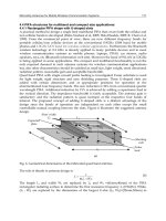
out
(a)
VD2
VG2
VDG2
VD1
VG1
(b)
Fig. 23. (a).Conventional cascode amplifier (b).Voltage waveforms versus time for V
G
=0.8V,
V
in
=0.8sin
t, and
=5.25GHz.
6.2 Self-biased cascode power stage
To overcome the breakdown voltage limitation problem of M2, a self-biased cascode
transistor is proposed as shown in Fig.24(a), which it allows RF swing at G2. This enables us
to design the PA such that both transistors experience the same maximum drain–gate
voltage. Consequently, we can have a larger signal swing at D2 before encountering hot
carrier degradation.
V
in
C
block
G1
R
g
V
G
RFC
V
DD
M1
M2
D1
D2
G2
C
block
V
out
R
b
C
b
(a)
VD2VG2
VD1
VD1
VDG2
(b)
Fig. 24. Operational waveforms of (a).Self-biased cascode amplifier (b).Voltage waveforms
versus time for V
G
=0.8V, V
in
=0.8sin
t, R
b
=0.75K, C
b
=2.4 pf,and
=5.25GHz.
The bias for G2 is provided by R
b
–C
b
network, for which no extra bondpad is required. The
dc voltage applied to G2 is the same as the dc voltage applied to D2. The RF swing at D2 is
attenuated by the low-pass nature of R
b
–C
b
network as shown in Fig.24(b). The values of R
b
and C
b
can be chosen for optimum performance and for equal gate–drain signal swings on
M1 and M2. As G2 follows the RF variation of D2 in both positive and negative swings
around its dc value, a non-optimal gain performance is obtained (compared with a cascode
with RF ground at G2). However, as long as both M1 and M2 go from saturation into triode
under large-signal operation, the maximum output power and PAE are not degraded. The
effect of the self-biased concept is demonstrated in Fig.24(b). Here, the same dimensions of
MobileandWirelessCommunications:Networklayerandcircuitleveldesign342
the devices are used as for the case presented in Fig. 23(b). A reduction of more than 20% in
the drain–gate voltage of M2 is actually obtained.
6.3 Boot-strapped cascode power stage
To further extend this idea, we can add a resistive-diode boosting so that the positive swing
of G2 can be made larger than the negative swing as shown in Fig. 25(a). By choosing the
value of R
d
and the size of the diode connected transistor M3, we can specify the threshold
voltage at which the R
d
–M3 starts conducting and boosting the positive swing at G2. This
extra path enables G2 to follow the rise in D2 with a smaller attenuation than the fall in D2.
During this transient response, the average charge stored on C
b
increases causing R
d
–M3 to
conduct for a smaller percentage of the duty cycle. The average voltage at G2 increases up to
the point where R
d
–M3 no longer conducts. In steady state, the R
d
–M3 path is off and the
positive and negative swings at G2 are equal. Fig. 25(b) shows the drain and gate voltages of
transistor M2 versus time for different values of R
d
. The voltage swing at D2 is not affected
by R
d
, and the peak-to-peak swing of VG2 depends on R
b
–C
b
and not R
d
. However, as the
value of R
d
is reduced, the average voltage of VG2 increases. In Class-E PA design, the
voltage swing can be about three times the supply voltage (with a larger positive swing than
negative around supply). In this situation, the bootstrapped cascode configuration can be
employed to have the same maximum voltage swings at gate–drain of M1 and M2.
Therefore, a larger supply voltage can be applied, resulting in a higher output power. For
Class-AB/B design, where the signal has roughly the same positive and negative swings
around the supply voltage, the self-biased cascade provides the required swing on G2.
V
in
C
block
G1
R
g
V
G
RFC
V
DD
M1
M2
D1
D2
G2
C
block
V
out
R
b
C
b
R
d
M3
(a)
VD2
VG2
VGD2
(b)
Fig. 25. (a). Bootstrapped cascode power stage. (b). Voltage waveforms.
7. Case Study–Implementation of a 5.25-GHz CMOS Cascode Power Amplifier
for 802.11a WLAN
In the case study, we investigate a 5.25-GHz highly integrated CMOS class-AB power
amplifier for IEEE 802.11a WLAN. The proposed power amplifier is implemented with a
two gain-stage structure which is followed by an off-chip output matching circuit.
Moreover, transistor-level compensation techniques are employed to improve the linearity.
The power amplifier is designed with an on-chip input matching circuit while the output
matching circuit translates the signal power from 50- to 20- load resistance. The
measured results indicate over 20% power-added efficiency, over 20-dBm output power,
and 28.6-dBm output IP3. All the specifications are based on 50- input impedance at 2.4V
supply voltage.
7.1 Introduction
Integration with a CMOS process is the key challenge for the state-of-the-art systems-on-a-
chip (SOC) design approach. Conventionally, wireless local area network (WLAN) has been
implemented with a multi-chip approach. However, the integration of baseband and RF
front-end circuits with a CMOS process is the most promising approach to achieve highly
integrated level, low power consumption, and low cost for a WLAN system. A challenging
functional block in designing a wireless communication transceiver is the power amplifier
due to the trade-offs between supply voltage, output power, power efficiency, and linearity,
which the problem may couple with spectrum efficiency and leading to an even more
difficult dilemma.
In order to achieve a higher spectrum-efficiency, the new OFDM (Orthogonal Frequency
Division Multiplexing) based WLAN standards use non-constant envelope modulation,
PowerAmplierDesignforHighSpectrum-EfciencyWirelessCommunications 343
the devices are used as for the case presented in Fig. 23(b). A reduction of more than 20% in
the drain–gate voltage of M2 is actually obtained.
6.3 Boot-strapped cascode power stage
To further extend this idea, we can add a resistive-diode boosting so that the positive swing
of G2 can be made larger than the negative swing as shown in Fig. 25(a). By choosing the
value of R
d
and the size of the diode connected transistor M3, we can specify the threshold
voltage at which the R
d
–M3 starts conducting and boosting the positive swing at G2. This
extra path enables G2 to follow the rise in D2 with a smaller attenuation than the fall in D2.
During this transient response, the average charge stored on C
b
increases causing R
d
–M3 to
conduct for a smaller percentage of the duty cycle. The average voltage at G2 increases up to
the point where R
d
–M3 no longer conducts. In steady state, the R
d
–M3 path is off and the
positive and negative swings at G2 are equal. Fig. 25(b) shows the drain and gate voltages of
transistor M2 versus time for different values of R
d
. The voltage swing at D2 is not affected
by R
d
, and the peak-to-peak swing of VG2 depends on R
b
–C
b
and not R
d
. However, as the
value of R
d
is reduced, the average voltage of VG2 increases. In Class-E PA design, the
voltage swing can be about three times the supply voltage (with a larger positive swing than
negative around supply). In this situation, the bootstrapped cascode configuration can be
employed to have the same maximum voltage swings at gate–drain of M1 and M2.
Therefore, a larger supply voltage can be applied, resulting in a higher output power. For
Class-AB/B design, where the signal has roughly the same positive and negative swings
around the supply voltage, the self-biased cascade provides the required swing on G2.
V
in
C
block
G1
R
g
V
G
RFC
V
DD
M1
M2
D1
D2
G2
C
block
V
out
R
b
C
b
R
d
M3
(a)
VD2
VG2
VGD2
(b)
Fig. 25. (a). Bootstrapped cascode power stage. (b). Voltage waveforms.
7. Case Study–Implementation of a 5.25-GHz CMOS Cascode Power Amplifier
for 802.11a WLAN
In the case study, we investigate a 5.25-GHz highly integrated CMOS class-AB power
amplifier for IEEE 802.11a WLAN. The proposed power amplifier is implemented with a
two gain-stage structure which is followed by an off-chip output matching circuit.
Moreover, transistor-level compensation techniques are employed to improve the linearity.
The power amplifier is designed with an on-chip input matching circuit while the output
matching circuit translates the signal power from 50- to 20- load resistance. The
measured results indicate over 20% power-added efficiency, over 20-dBm output power,
and 28.6-dBm output IP3. All the specifications are based on 50- input impedance at 2.4V
supply voltage.
7.1 Introduction
Integration with a CMOS process is the key challenge for the state-of-the-art systems-on-a-
chip (SOC) design approach. Conventionally, wireless local area network (WLAN) has been
implemented with a multi-chip approach. However, the integration of baseband and RF
front-end circuits with a CMOS process is the most promising approach to achieve highly
integrated level, low power consumption, and low cost for a WLAN system. A challenging
functional block in designing a wireless communication transceiver is the power amplifier
due to the trade-offs between supply voltage, output power, power efficiency, and linearity,
which the problem may couple with spectrum efficiency and leading to an even more
difficult dilemma.
In order to achieve a higher spectrum-efficiency, the new OFDM (Orthogonal Frequency
Division Multiplexing) based WLAN standards use non-constant envelope modulation,
MobileandWirelessCommunications:Networklayerandcircuitleveldesign344
which the linearity of the power amplifier is a key parameter as it is closely related to power
consumption and distortion. Moreover, class-AB power amplifiers are widely used in
wireless transceiver design due to their high efficiency and relatively high linearity.
Transistor-level compensation techniques to enhance the linearity of a CMOS power
amplifier are investigated in this case study. On the other hand, cascode configuration has
been employed to eliminate the effects of oxide breakdown voltage and hot carrier
degradation, which allows the use of a higher supply voltage. A self-biased technique with
thin-oxide MOS is presented, which it can relax the restriction due to the hot carrier
degradation in power amplifiers and alleviate the conventional requirement of using thick-
oxide transistors.
7.2 Implementation of a two-stage cascode differential power amplifier
Some transistor-level linearization techniques have been employed in the radio-frequency
PA design including nonlinear capacitance cancellation in CMOS PA design, PMOS
cancellation, parallel diode with a bias feed resistance, and varactor cancellation. In this case
study, a diode linearizer as presented in Section 5.3 is integrated in the proposed class-AB
PA design, which it can effectively reduce the gain compression and phase distortion. In
order to increase the power gain of the CMOS PA and reduce the current required to charge
and discharge the parasitic capacitors of these nodes, the inductor Ltank is employed across
the differential cascode nodes between drain and source connections, which acts as a
resonant tank at these nodes as shown in Fig. 21 of Section 5.4.
The two main issues in the design of power amplifiers in deep-submicron CMOS
technologies, namely, the oxide breakdown and the hot carrier effect, which become even
worse as the technology scales down. The oxide breakdown is a catastrophic effect and sets
a limitation of the maximum signal swing on the drain. The hot carrier effect increases the
threshold voltage and consequently degrades the performance of a device. To avoid hot
carrier degradation, the operating voltage is usually based on dc/transient reliability tests.
For production requirements, the voltage is 5%–10% above the maximum allowed supply
voltage to ensure a product lifetime. For a 0.18-m process, this leads to a maximum dc
drain-to-gate voltage of approximately 2V.
Cascode configuration and thick-oxide transistors have been employed to eliminate the
effects of oxide breakdown voltage and the hot carrier degradation, which allow the use of a
higher supply voltage. Under large signal operation, the voltage swing across the gate and
drain nodes of the common-gate transistor becomes larger than that of the common-source
transistor. Therefore, the common-gate transistor becomes the bottleneck in terms of
breakdown or hot carrier degradation. Since the characteristic of thick-oxide devices is
equivalent to a device of 0.35-m process, a combination of standard and thick-oxide
devices (standard device for the common-source and thick-oxide device for the common-
gate) can tolerate a much higher voltage, which was demonstrated in the implementation of
a 900-MHz, 0.2-m CMOS cascode power stage.
The power amplifier in this case study operates at 5.15GHz-5.35 GHz frequency band, the
maximum output power level is over 20dBm, and drain efficiency is over 20%. Moreover,
the power amplifier employs a NMOS device to compensate the nonlinear input capacitance
variation. By taking advantage of the NMOS device, the nonlinear capacitance can be
compensated to nearly constant in the input of the common source device, which in turn
improves the linearity. Miller’s capacitance effect has also been alleviated by the
employment of the two-stage cascode differential architecture. Furthermore, the fully
differential topology can bring the advantages of even order harmonics suppression and
better immunity against noise from power supply and the lossy substrate. Note that for a
0.18-m CMOS technology, the cut-off frequency f
t
exceeds 60GHz, the minimum noise
figure NF
min
is below 0.5dB and a threshold voltage of 0.4V, which is a promising technology
to implement a high-frequency PA operating at the frequency band.
On the other hand, a self-biased cascode structure presented in Section 6.2 does not
necessitate thick-oxide transistors since it can have a larger signal swing at node D2 before
encountering hot carrier degradation and this structure is employed in our power amplifier
design to alleviate the hot carrier effect.
(a). Matching Network with Bond-Wire and Pad
The bond-wire can be modeled with the series connection of an inductor and a resistor,
which the corresponding inductance and resistance are about 0.8nH/mm and 0.16Ω/nH,
respectively for the diameter of 25-m bond-wires. Moreover, constructed from a stack of
metal6 (20kA in height), via5 (6kA), and metal5 (5.8kA) layers, the pad occupies an area of
8080m
2
, which is equivalent to the series connection of a 625Ω-resistor and a 0.0625pF-
capacitor to ground. Therefore, the bond-wire and pad can be modeled with the equivalent
circuit which can be easily matched with a -type matching network.
(b). Driver Stage
The first stage of the power amplifier is configured at class-A operation to provide the
sufficient gain and linearity for the design. The schematic of the stage is shown in Fig.26,
which the center frequency is determined by the LC high-pass matching network
constructed with L
1
, C
1
, L
2
, C
2
, and parasitic capacitors. L
1
, L
2
, C
p3
, and C
p4
perform the inter-
stage impedance matching at 5.15GHz-5.35GHz.
Rb1
M2M1
M3
L1
Cd1
VDD1
Cd2
VDD1
Vbias1
Rb2
Cb1 Cb2
C1
Cp3
Bondwire
Bondwire
M4
IN+
R1 R2
Cp1
Bondwire
Cp4
L2
C2
IN-
L_in1
C_in1
L_in2
C_in2
OP+ OP-
Fig. 26. Schematic of the driver stage.
PowerAmplierDesignforHighSpectrum-EfciencyWirelessCommunications 345
which the linearity of the power amplifier is a key parameter as it is closely related to power
consumption and distortion. Moreover, class-AB power amplifiers are widely used in
wireless transceiver design due to their high efficiency and relatively high linearity.
Transistor-level compensation techniques to enhance the linearity of a CMOS power
amplifier are investigated in this case study. On the other hand, cascode configuration has
been employed to eliminate the effects of oxide breakdown voltage and hot carrier
degradation, which allows the use of a higher supply voltage. A self-biased technique with
thin-oxide MOS is presented, which it can relax the restriction due to the hot carrier
degradation in power amplifiers and alleviate the conventional requirement of using thick-
oxide transistors.
7.2 Implementation of a two-stage cascode differential power amplifier
Some transistor-level linearization techniques have been employed in the radio-frequency
PA design including nonlinear capacitance cancellation in CMOS PA design, PMOS
cancellation, parallel diode with a bias feed resistance, and varactor cancellation. In this case
study, a diode linearizer as presented in Section 5.3 is integrated in the proposed class-AB
PA design, which it can effectively reduce the gain compression and phase distortion. In
order to increase the power gain of the CMOS PA and reduce the current required to charge
and discharge the parasitic capacitors of these nodes, the inductor Ltank is employed across
the differential cascode nodes between drain and source connections, which acts as a
resonant tank at these nodes as shown in Fig. 21 of Section 5.4.
The two main issues in the design of power amplifiers in deep-submicron CMOS
technologies, namely, the oxide breakdown and the hot carrier effect, which become even
worse as the technology scales down. The oxide breakdown is a catastrophic effect and sets
a limitation of the maximum signal swing on the drain. The hot carrier effect increases the
threshold voltage and consequently degrades the performance of a device. To avoid hot
carrier degradation, the operating voltage is usually based on dc/transient reliability tests.
For production requirements, the voltage is 5%–10% above the maximum allowed supply
voltage to ensure a product lifetime. For a 0.18-m process, this leads to a maximum dc
drain-to-gate voltage of approximately 2V.
Cascode configuration and thick-oxide transistors have been employed to eliminate the
effects of oxide breakdown voltage and the hot carrier degradation, which allow the use of a
higher supply voltage. Under large signal operation, the voltage swing across the gate and
drain nodes of the common-gate transistor becomes larger than that of the common-source
transistor. Therefore, the common-gate transistor becomes the bottleneck in terms of
breakdown or hot carrier degradation. Since the characteristic of thick-oxide devices is
equivalent to a device of 0.35-m process, a combination of standard and thick-oxide
devices (standard device for the common-source and thick-oxide device for the common-
gate) can tolerate a much higher voltage, which was demonstrated in the implementation of
a 900-MHz, 0.2-m CMOS cascode power stage.
The power amplifier in this case study operates at 5.15GHz-5.35 GHz frequency band, the
maximum output power level is over 20dBm, and drain efficiency is over 20%. Moreover,
the power amplifier employs a NMOS device to compensate the nonlinear input capacitance
variation. By taking advantage of the NMOS device, the nonlinear capacitance can be
compensated to nearly constant in the input of the common source device, which in turn
improves the linearity. Miller’s capacitance effect has also been alleviated by the
employment of the two-stage cascode differential architecture. Furthermore, the fully
differential topology can bring the advantages of even order harmonics suppression and
better immunity against noise from power supply and the lossy substrate. Note that for a
0.18-m CMOS technology, the cut-off frequency f
t
exceeds 60GHz, the minimum noise
figure NF
min
is below 0.5dB and a threshold voltage of 0.4V, which is a promising technology
to implement a high-frequency PA operating at the frequency band.
On the other hand, a self-biased cascode structure presented in Section 6.2 does not
necessitate thick-oxide transistors since it can have a larger signal swing at node D2 before
encountering hot carrier degradation and this structure is employed in our power amplifier
design to alleviate the hot carrier effect.
(a). Matching Network with Bond-Wire and Pad
The bond-wire can be modeled with the series connection of an inductor and a resistor,
which the corresponding inductance and resistance are about 0.8nH/mm and 0.16Ω/nH,
respectively for the diameter of 25-m bond-wires. Moreover, constructed from a stack of
metal6 (20kA in height), via5 (6kA), and metal5 (5.8kA) layers, the pad occupies an area of
8080m
2
, which is equivalent to the series connection of a 625Ω-resistor and a 0.0625pF-
capacitor to ground. Therefore, the bond-wire and pad can be modeled with the equivalent
circuit which can be easily matched with a -type matching network.
(b). Driver Stage
The first stage of the power amplifier is configured at class-A operation to provide the
sufficient gain and linearity for the design. The schematic of the stage is shown in Fig.26,
which the center frequency is determined by the LC high-pass matching network
constructed with L
1
, C
1
, L
2
, C
2
, and parasitic capacitors. L
1
, L
2
, C
p3
, and C
p4
perform the inter-
stage impedance matching at 5.15GHz-5.35GHz.
Rb1
M2M1
M3
L1
Cd1
VDD1
Cd2
VDD1
Vbias1
Rb2
Cb1 Cb2
C1
Cp3
Bondwire
Bondwire
M4
IN+
R1 R2
Cp1
Bondwire
Cp4
L2
C2
IN-
L_in1
C_in1
L_in2
C_in2
OP+ OP-
Fig. 26. Schematic of the driver stage.