Radio Frequency Identification Fundamentals and Applications, Design Methods and Solutions Part 12 ppt
Bạn đang xem bản rút gọn của tài liệu. Xem và tải ngay bản đầy đủ của tài liệu tại đây (2.29 MB, 25 trang )
Radio Frequency Identification Fundamentals and Applications, Design Methods and Solutions
266
Although metals like copper (Hong & Wagner, 2000) and gold (Molesa et al., 2003) have
been used for inkjet printing applications, direct inkjet printing of conductive silver tracks
onto flexible substrates has gained interest due to silver having the lowest resistivity value
and the relatively simple synthesis of silver nanoparticles (Schmid, 2004). Therefore, it has
been used for many applications, such as interconnections for a circuitry on a printed circuit
board (Szczech et al., 2002), disposable displays and radio frequency identification (RFID)
tags (Huang et al., 2004; Potyrailo et al., 2009), organic thin-film transistors (Kim et al., 2007;
Gamerith et al., 2007), and electrochromic devices (Shim et al., 2008).
This chapter will describe how inkjet printing techniques can be used for the fabrication of
conductive tracks on a polymer substrate. The selective sintering of inkjet printed silver
nanoparticles is described by using microwave radiation. This not only sinters the particles
into a conductive feature, but it also reduces the sintering time significantly from hours to
minutes or even seconds. Furthermore, techniques to improve the printing resolution will be
discussed and the fabrication of conductive tracks of 40 µm wide will described.
Before going in detail on inkjet printing of advanced nanoparticle inks, we first review the
history of inkjet printing.
2. Historical overview of inkjet printing
The origin of inkjet printing goes back to the eighteenth century when Jean-Antoine Nollet
published his experiments on the effect of static electricity on a stream of droplets in 1749
(Nollet & Watson, 1749). Almost a century later, in 1833, Felix Savart discovered the basics
for the technique used in modern inkjet printers: an acoustic energy can break up a laminar
flow-jet into a train of droplets (Savart, 1833). It was, however, only in 1858 that the first
practical inkjet device was invented by William Thomson, later known as Lord Kelvin
(Thomson, 1867). This machine was called the Siphon recorder and was used for automatic
recordings of telegraph messages.
The Belgian physicist Joseph Plateau and the English physicist Lord Rayleigh studied the
break-up of liquid streams and are, therefore, seen as the founders of modern inkjet printing
technology. The break-up of a liquid jet takes place because the surface energy of a liquid
sphere is smaller than that of a cylinder, while having the same volume – see Figure 1
(Goedde & Yuen, 1970).
Fig. 1. Break-up of a laminar flow-jet into a train of droplets, because of Rayleigh-Plateau
instability (cm scale). Reprinted from (Goedde & Yuen, 1970).
When applying an acoustic energy, the frequency of the mechanical vibrations is
approximately equal to the spontaneous drop-formation rate. Subsequently, the drop-
formation process is synchronised by the forced mechanical vibration and therefore
produces ink drops of uniform mass. Lord Rayleigh calculated a characteristic wavelength λ
for a fluid stream and jet orifice diameter d given by (Rayleigh, 1878):
Inkjet Printing and Alternative Sintering of Narrow Conductive Tracks
on Flexible Substrates for Plastic Electronic Applications
267
4.443d
λ
=
(1)
The numerical value was later slightly corrected to 4.508 (Bogy, 1979). However, it took
another 50 years before the first design of a continuous inkjet printer, based on Rayleigh’s
findings, was filed as a patent by Rune Elmqvist (Elmqvist, 1951). He developed the first
inkjet electrocardiogram printer that was marketed under the name Mingograf by Elema-
Schönander in Sweden and Oscillomink by Siemens in Germany (Kamphoefner, 1972).
In the beginning of the 1960s, two continuous inkjet (CIJ) systems were developed
simultaneously, with a difference only in function of the electrical driving signals (Keeling,
1981). The first system was developed by Richard Sweet at Stanford University. He made a
high frequency oscillograph, where droplets were formed at a rate of 100 kHz and
controlled with respect to their direction by the electrical signal (Sweet, 1965). Later, in 1968,
the A. B. Dick Company elaborated upon Sweet’s invention to produce a device that was
used for character printing and named it the Videojet 9600: this was the first commercial
continuous inkjet printer. In parallel at the Lund Institute of Technology in Sweden, Hertz
et al. had developed a similar system where an electrical signal was used to disperse the
droplets into a mist, which enables frequencies up to 500 kHz (Hertz & Simonsson, 1969).
However, since their technique used a narrower nozzle diameter, 10 µm versus 50 µm, the
chance of nozzle clogging was greater (Heinzl & Hertz, 1985).
Instead of firing droplets in a continuous method, it is also possible to produce droplets
when required, hence an impulse jet, or better known as drop-on-demand (DoD). In the late
1940s, Clarence Hansell invented the DoD device, at the Radio Corporation of America
(Hansell, 1950). Figure 2 shows the schematics of his invention, which was never developed
into a commercial product at that time. It took until 1971 when the Casio Company released
the model 500 Typuter, which was an electrostatic pull DoD device.
Fig. 2. Schematic drawing of the first drop-on-demand piezoelectric device. Reprinted from
(Hansell, 1950).
Despite the fact that the basis of thermal inkjet (TIJ) DoD devices in the form of the sudden
stream printer had already been developed in 1965 at the Sperry Rand Company (Naiman,
1965), this idea was picked up much later by the Canon company, when in 1979 they filed
the patent for the first thermal inkjet printhead (Endo et al., 1979). Simultaneously, Hewlett-
Packard independently developed a similar technology that was first filed in 1981 (Vaught
et al., 1984). Thermal inkjet printers are actuated by a water vapour bubble, hence their name
Radio Frequency Identification Fundamentals and Applications, Design Methods and Solutions
268
bubble jet. The bubble is created by a thermal transducer that heats the ink above its boiling
point and, thereby, causes a local expansion of the ink, resulting in droplet formation. The
location of the thermal transducer can be either at the top of the reservoir – as used by HP –
or at its side, which is the technique Canon uses.
At the beginning of the 1970s the piezoelectric inkjet (PIJ) DoD system was developed
(Carnahan & Hou, 1970). At the Philips laboratories in Hamburg printers operating on the
DoD principle were the subject of investigation for several years (Döring, 1982). In 1981 the
P2131 printhead was developed for the Philips P2000T microcomputer, which had a Z80
microprocessor running at 2.5 MHz. Later the inkjet activities of Philips in Hamburg were
continued under the spin-off company Microdrop (nowadays Microdrop Technologies,
www.microdrop.com). The first piezoelectric DoD printer on the market was the serial
character printer Siemens PT80 in 1977.
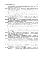
Four different modes for droplet generation by means of a piezoelectric device were
developed in the 1970s, which are summarised in Figure 3, and further explained below
(Brünahl & Grishin, 2002).
(d) Shear mode(c) Push mode(b) Bend mode(a) Squeeze mode
Fig. 3. Different piezoelectric drop-on-demand technologies. Reprinted from (Brünahl, 2002).
Firstly, the squeeze method, invented by Steven Zoltan (Zoltan, 1972), uses a hollow tube of
piezoelectric material, that squeezes the ink chamber upon an applied voltage (Figure 3a).
Secondly, the bend-mode (Figure 3b) uses the bending of a wall of the ink chamber as
method for droplet ejection and was discovered simultaneously by Stemme of the Chalmers
University in Sweden (Stemme, 1972) and Kyser of the Silonics company in the USA (Kyser
& Sears, 1976). The third mode is the pushing method by Howkins (Figure 3c), where a
piezoelectric element pushes against an ink chamber wall to expel droplets (Howkins, 1984).
Finally, the shear-mode (Figure 3d) was found by Fishbeck, where the electric field is
designed to be perpendicular to the polarization of the piezo-ceramics (Fishbeck & Wright,
1986).
Besides the continuous and drop-on-demand inkjet technique, a third type of inkjet printing
is known, which is based on the electrostatic generation of ink droplets (Winston, 1962). The
system is weakly pressurised, causing the formation of a convex meniscus of a conductive
ink. An electrostatic force, which exceeds the meniscus’ surface tension, is applied between
the ink hemisphere and the flat electrode by setting a voltage. Depending on the nature of
the electrical potential the system can either be a continuous or drop-on-demand inkjet: the
pulse duration determines whether the ejected ink is a continuous stream or a stream of
droplets. As a summary of the different inkjet printing technologies, Figure 4 schematically
represents a classification thereof.
Inkjet Printing and Alternative Sintering of Narrow Conductive Tracks
on Flexible Substrates for Plastic Electronic Applications
269
Continuous Drop-on-Demand
Inkjet technology
Undeflected Deflected Unvibrated
Binary Multiple
Acoustic Piezo Electrostatic Thermal
Top shooter Side shooter
Shear PushBend Squeeze
Fig. 4. Classification of inkjet printing technologies, adapted from (Le, 1998).
Although inkjet printing offers a simple and direct method of electronic controlled writing
with many advantages, including high speed production, silent, non-impact and fully
electronic operation, inkjet printers failed to be commercially successful in their beginning:
print quality as well as reliability and costs were hard to combine in a single printing
technique. Whereas CIJ provides high throughput, it also requires high costs to gain good
quality. Nowadays this technique is used in lower quality and high speed graphical
applications such as textile printing and labelling. On the other hand, PIJ usually provides
good quality but lacks high printing velocities: although this can be compensated for by
using multi nozzle systems, but this increases the production costs as well. TIJ changed the
image of inkjet printing dramatically. Not only could thermal transducers be manufactured
in much smaller sizes, since they require a simple resistor instead of a piezoelectric element,
but also at lower costs. Therefore, thermal inkjet printers dominate the colour printing
market nowadays (Kipphan, 2004).
In scientific research piezoelectric DoD inkjet systems are mainly used because of their
ability to dispense a wide variety of solvents, whereas thermal DoD printers are more
compatible with aqueous solutions (Gans et al., 2004). Furthermore, the rapid and localised
heating of the ink within TIJ induces thermal stress on the ink. Nevertheless, research has
been conducted using TIJ printers, for example to form conductive patterns, either by
printing the water soluble conjugated polymer PEDOT:PSS (Yoshioka & Jabbour, 2006), or
by printing aqueous solutions of conductive multi-walled carbon nanotubes (Kordás, 2006).
3. Methods for sintering nanoparticle inks
Conductive materials that are suitable for inkjet printing can be either solution-based or
particle based. The former one is usually based on a metallo-organic decomposition (MOD)
ink, in particular silver neodecanoate dissolved in an aromatic solvent (Dearden et al., 2005;
Smith et al., 2006). These MOD inks have been used for inkjet printing since the late 1980s
(Vest et al., 1983). In order to obtain metal features, a conversion of organometallic silver
inks is required, which usually takes place at relatively low temperatures below 200 °C (Wu
et al., 2007), although temperatures below 150 °C have been reported as well (Smith et al.,
2006, Perelaer et al., 2009a). The typical metal loading of organometallic inks is 10 to 20 wt%.
Radio Frequency Identification Fundamentals and Applications, Design Methods and Solutions
270
In contrast to metal containing inks based on complexes, inks consisting of a dispersion of
nanoparticles have been investigated as well, with the ability to have a silver loading
>20 wt% being one of the reasons. Such a dispersion contains metallic nanoparticles with a
diameter between 1 and 100 nm. It was found that gold nanoparticles with a diameter below
100 nm reveal a significant reduction in their melting temperature (Buffat & Borel, 1976), as
depicted in Figure 5a from their bulk melting temperature of 1064 °C to well below 300 °C
when the diameter is below 5 nm. Ten years later, Allen and co-workers showed that this
reduction of the melting temperature is also valid for other metals, including tin, lead and
bismuth (Allen et al., 1986). In a graph of the melting temperature against the reciprocal of
the particle radius the data exhibit near-linear relationships, as depicted in Figure 5b. It was
also found that plates instead of spheres do not show a reduced melting temperature. This
suggests that the size dependence of melting particles is related to the internal hydrostatic
pressure caused by the surface stress and by the large surface curvature of the particles, but
not by the planar surfaces of platelets.
(a) (b)
Inverse radius (nm
-1
)
Diameter (Å)
Fig. 5. Influence of the gold (a) and lead, bismuth, tin and indium (b) particle diameter on
their melting temperature. Reprinted from (Buffat & Borel, 1976; Allen et al., 1986),
respectively.
Given the reduced melting temperature of nanoparticles, these particles represent ideal
candidates for dispersion in a liquid medium and, subsequently, for inkjet printing.
However, when two or more particles are in contact, merging of nanoparticles into larger
clusters can take place due to the large surface curvature of the individual nanoparticles.
This process is called sintering and takes place with small particles within the medium and
at room temperature. Therefore, the nanoparticles have to be protected by a shell to prevent
agglomeration in solution and to obtain a stable colloidal dispersion, as schematically
depicted in Figure 6 (Lee et al., 2006).
In non-polar solvents usually long alkyl chains with a polar head, like thiols, amines or
carboxylic acids, are used to stabilise the nanoparticles (Perelaer et al., 2008a). Steric
stabilisation of these particles in non-polar solvents substantially screens van der Waals
attractions and introduces steep steric repulsion between the particles at contact, which
avoids agglomeration (Bönnemann & Richards, 2001). In addition, organic binders are often
added to the ink to assure not only mechanical integrity and adhesion to the substrate, but
also to promote the printability of the ink.
Inkjet Printing and Alternative Sintering of Narrow Conductive Tracks
on Flexible Substrates for Plastic Electronic Applications
271
Fig. 6. Schematic illustration of a silver nanoparticle with carboxylic acids as capping agent.
After silver containing inks have been inkjet printed, and solvent evaporation has occurred,
another processing step is necessary to form conductive features since the organic shell
inhibits close contact of the nanoparticles. Although evaporation of the solvent forces the
particles close together, conductivity only arises when metallic contact between the particles
is present and a continuous percolating network is formed throughout the printed feature.
An organic layer between the silver particles as thin as a few nanometers is sufficient to
prevent electrons moving from one particle to the other (Lovinger, 1979). The adsorbed
dispersant stays on the surface of the particles and, typically, is removed by an increase in
temperature.
Mostly, particulate features have been rendered conductive by applying heat. This thermal
sintering method usually requires temperatures above 200 °C (Chou et al., 2005). Other
techniques that have been used to for conductive features include LASER sintering (Ko et al.,
2007), exposure to UV radiation (Radivojevic et al., 2006), high temperature plasma sintering
(Groza et al., 1992) and pulse electric current sintering (Xie et al., 2003). However, most of
these techniques are not suitable for polymer substrate materials due to the large overall
thermal energy impact. In particular, when using common polymer substrates, like
polycarbonate (PC) and polyethylene terephthalate (PET), that have their glass transition
temperature (Tg) well below the temperature required for sintering. In fact, only the
expensive high-performance polymers, like polytetrafluoroethylene, polyetheretherketone
and polyimide (PI) can be used at high temperatures, which represents a serious drawback
for implementation in a large area production of plastic electronics and is not favourable in
terms of costs.
In the field of sintering two properties are very important: firstly, the lowest temperature at
which printed features become conductive, which is mainly determined by the organic
additives in the ink (Liang et al., 2004). Secondly, obtaining the lowest possible resistance of
the printed features at the lowest possible temperature. To achieve a low resistance,
sintering of the particles is required to transform the initially very small contact areas to
thicker necks and, eventually, to a dense layer. High conductivities, hence low resistance,
can then be obtained through the formation of large necks, which decrease constriction
resistance and eventually form a metallic crystal structure with a low number of grain
boundaries.
Radio Frequency Identification Fundamentals and Applications, Design Methods and Solutions
272
In the low temperature regime, the driving forces for sintering are mainly surface energy
reduction due to the particles large surface-to-volume ratio, a process known as Ostwald
ripening (Ostwald, 1896). This process triggers surface and grain boundary diffusion rather
than bulk diffusion within the coalesced particles, as schematically depicted in Figure 7.
Grain boundary diffusion allows for neck formation and neck radii increase, which is
diminished by the energy required for grain boundary creation (Greer et al., 2007).
Therefore, the process will stall eventually, leaving a porous structure behind, which leads
to lower conductivity values when compared to the bulk material.
1. Lattice diffusion (no densification)
2. Surface diffusion (no densification)
3. Through-lattice diffusion (densification)
4. Grain boundary diffusion (densification)
1
4
3
2
Fig. 7. A schematic representation of various atomic diffusion paths between two contacting
particles. Paths 1 and 2 do not produce any shrinkage whilst paths 3 and 4 enable the sphere
centres to approach one another, resulting in densification. Reprinted from (Greer et al.,
2007).
At high temperatures, however, lattice diffusion leads to closure of pores and densification.
However, long sintering times are necessary for creating dense conductive features in a
thermal process and obstruct the feasibility for an efficient industrial production processes.
In order to reduce production costs, alternative techniques that sinter silver nanoparticles in
a selective manner without harming the underlying polymer substrate need to be found.
The properties of thermal sintering will be discussed in the next paragraphs, after which a
technique that uses microwave radiation will be described as possible candidate for a
selective sintering process.
3.1 Thermal sintering of inkjet printed silver lines
A major concern with printed electronics involves not only the control of the morphology of
the tracks (Smith et al., 2006; Berg et al., 2007), but also the stability and adhesion of the
obtained conductive tracks, although this has scarcely been investigated (Kim et al., 2006).
However, the main focus in plastic electronics lies in the low curing temperature of the
conductive ink. For particle-based inks, the curing temperature is defined as the
temperature where particles loose their organic shell and start showing conductance by
direct physical contact. Whereas sintering (which is often mistakenly used instead of curing
temperature) takes place at a higher temperature when all the organic material has been
burnt off and necks begin to form between particles. The lowest temperature at which
printed features become conductive is mainly determined by the organic additives in the ink
(Liang et al., 2004). Often high temperatures – typically up to 300 °C – are required to burn
off the organic additives and to stimulate the sintering process to realise a more densely
Inkjet Printing and Alternative Sintering of Narrow Conductive Tracks
on Flexible Substrates for Plastic Electronic Applications
273
packed silver layer and a lower resistivity (Smith et al., 2006; Yoshioka & Jabbour, 2006). It is
therefore of utmost importance if further progress is to be made to identify an optimum
between time, temperature and the obtained conductivity.
In order to reveal first structure-property relationships and to later develop the new ink, the
sintering behaviour of inkjet printed silver tracks based on commercial inks was studied.
The critical curing temperature is defined in this case as the temperature at which the
sample becomes conductive, i.e. having a resistance lower than 40 MΩ which is the upper
measuring limit of the used multi-meter. Single lines with a length of 1 cm of the specific ink
were inkjet printed onto boron-silicate glass and subsequently heated to 650 °C in an oven at
a heating rate of 10 °C min
-1
. During heating the resistance was measured online in a semi-
continuous way, by measuring every 2 seconds. Using this dynamic scan approach,
differences between the various inks can be determined.
Typical resistance results for the Cabot and Nippon inks are shown in Figure 8a and Figure
9a, respectively. The resistance of the lines for both inks decreases rapidly when heated
above the critical curing temperature. The critical curing temperature for the Cabot silver
ink is 194 °C, which is lower than the Nippon ink, 269 °C. According to the particle size
measurements, 52.4 ± 11.0 nm for the Cabot ink and 10.8 ± 6.7 nm for the Nippon ink (see
Figure 8b and Figure 9b), it was expected that the smaller particles would sinter at the lower
temperature because of their higher sintering activity (Buffat & Borel, 1976; Allen et al.,
0 100 200 300 400 500 600 700
20
30
40
50
60
70
80
90
100
Resistance (Ω)
Mass (%)
Temperature (°C)
10
0
10
1
10
2
10
3
10
4
10
5
10
6
10
7
10
8
10
9
(a)
10 20 30 40 50 60 70 80 90
0
5
10
15
20
25
30
35
% particles
Particle size (nm)
(b)
50 nm50 nm
(c)
20 µm
500 nm
Fig. 8. Resistance over a single inkjet printed line with a length of 1 cm as function of
temperature and thermogravimetric analysis (TGA) of Cabot silver ink (a). Transmission
electron microscopy (TEM) image and particle size distribution of Cabot silver nanoparticles
(b). Scanning electron microscopy (SEM) image of sintered Cabot silver nanoparticles at a
temperature of 650 °C (c). Reprinted from (Perelaer et al., 2008a).
Radio Frequency Identification Fundamentals and Applications, Design Methods and Solutions
274
1986). This indicates that the organic additives in the ink strongly affect the critical curing
temperature. Unfortunately, the nature of the organic additives in these commercially
available inks is not disclosed.
To elaborate on this the mass decrease upon heating by means of thermogravimetric
analysis (TGA) was also investigated. It should be mentioned that all inks have been dried
prior to measuring by heating to 50 °C for 20 minutes, which removed volatile solvents. The
TGA curve for Cabot silver ink shows a decrease of 72 wt%, which is not only the organic
binder that is around each nanoparticle but also the non-volatile solvent ethylene glycol
which is present in the ink (Figure 8a). The critical curing temperature corresponds to a
temperature at which the initial sharp weight loss slows down. The first step in the removal
of the organic materials has ended at this temperature. The steep decrease in resistance
relates to the temperature range in which the last part of the organics is burnt off.
Apparently, all organics have to be removed before the sintering of the Ag particles can
proceed in a fast way. This is indicative of an additive that is strongly adsorbed on the
surface of the silver particles.
The lines printed with the Nippon ink reveal a critical curing temperature and a fast
decrease in resistance when only about 15% of the organic additives are removed (Figure
9a). Obviously, these particles can make metallic contact long before all the organics are
gone. In addition, sintering proceeds very fast due to the small particle size. At the
temperature where the organics have been completely burnt off, only a small additional
decrease in resistance occurs. In this ink, only a minor part of the organic additives
interferes with the sintering process but it does shift the critical curing temperature to a high
value. For both inks, however, the resistance value levels off at a certain temperature. At this
temperature all organics are burnt off and, apparently, the sintering process has ended and a
silver layer with a final density and morphology has formed.
Figure 8c shows a scanning electron microscopy (SEM) image of a Cabot silver track that has
been heated to 650 °C. As can be seen the particles have sintered to a dense continuous line.
0 100 200 300 400 500 600 700
20
30
40
50
60
70
80
90
100
Resistance (Ω)
Mass (%)
Temperature (°C)
10
0
10
1
10
2
10
3
10
4
10
5
10
6
10
7
10
8
10
9
(a)
0 5 10 15 20 25 30
0
2
4
6
8
10
12
% particles
Particle size (nm)
(b)
50 nm50 nm
Fig. 9. Resistance over a single inkjet printed line with a length of 1 cm as function of
temperature and thermogravimetric analysis (TGA) of Nippon silver ink (a). Transmission
electron microscopy (TEM) image and particle size distribution of Nippon silver
nanoparticles (b). Reprinted from (Perelaer et al., 2008a).
The electrical resistivity ρ of the inkjet printed lines was calculated after heating to 650 °C,
using
Inkjet Printing and Alternative Sintering of Narrow Conductive Tracks
on Flexible Substrates for Plastic Electronic Applications
275
A/AR
⋅
=
ρ
(2)
with the lines resistance R, its length λ, and its cross sectional area A, and compared to the
value of bulk silver (1.59 × 10
-8
Ω m) (Fuller et al., 2002). The resistivity was calculated to be
3.10 × 10
-8
Ω m (51%) and 3.06 × 10
-8
Ω m (52%) for Cabot and Nippon, respectively. The
values in brackets indicate the percentage of conductivity (1/ρ) of bulk silver.
In summary, typical sintering temperatures of above 200 °C are required, which limits the
usage of many potentially interesting substrate materials, such as common polymer foils or
paper. Moreover, the long sintering time of 60 minutes or more that is generally required
according to the ink supplier to create conductive features, also obstruct industrial
implementation, e.g. roll-2-roll applications.
One selective technique for nanoparticle sintering that has been described in literature is
based on an Argon ion LASER beam that follows the as-printed feature and selectively
sinters the central region. Features with a line width smaller than 10 µm have been created
with this technique (Ko et al., 2007). However, the large overall thermal energy impact
together with the low writing speed of 0.2 mm s
-1
of the translational stage are limiting
factors (Chung et al., 2004). In fact, with this particularly technique low writing speeds are
required for good electrical behaviour since the resistance increases for faster write speeds
(Smith et al., 2006). Thus, other techniques have to be used in order to facilitate fast and
selective heating of the printed structures only. Microwave heating fulfils these
requirements (Nüchter et al., 2004).
3.2 Selective sintering of silver nanoparticle by using microwave radiation
Microwave heating is widely used for sintering of dielectric materials, conductive materials,
and in synthetic chemistry (Wiesbrock et al., 2004). It offers the advantage of uniform, fast
and volumetric heating.
The dielectric response to a field is given by the complex permittivity
0
'"'
εω
σ
εεεε
⋅
+=+= ii
r
(3)
where ε’ accounts for energy storage, ε” for energy loss of the incident electromagnetic wave
or so-called dissipation, i the imaginary unit, σ the conductivity and ω the angular
frequency. The ratio of the imaginary to the real part of the permittivity defines the
capability of the material to dissipate power compared to energy storage and is generally
know as the loss tangent:
"
tan
'
ε
δ
ε
=
(4)
Depending on their loss characteristic, and thus their conductivity, materials can be opaque,
transparent or an absorber. For bulk metals, being good electronic conductors, no internal
electrical field is generated and the induced electrical charge remains at the surface of the
sample (Agrawal, 2006). Consequently, metals reflect microwaves; while bulk metals do not
absorb until they have been heated to about 500 °C, powders with particle sizes within the
micrometer-region are rather good absorbers (Cheng, 1989). It is believed that the
conductive particle interaction with microwave radiation, i.e. inductive coupling, is mainly
based on Maxwell-Wagner polarisation, which results from the accumulation of charge at
Radio Frequency Identification Fundamentals and Applications, Design Methods and Solutions
276
the materials interfaces, electric conduction, and eddy currents. However, the main reasons
for successful heating of metallic particles through microwave radiation are not yet fully
understood.
The penetration depth d is defined as the distance into the material at which the incident
power is reduced to 1/e (36.8%) of the surface value and is given by
0
1
2"
c
d
f
f
ε
πε
π
μσ
== (5)
with c being the speed of light and f the frequency of the microwave radiation. Typically,
highly conductive materials (e.g. metals) have a very small penetration depth. For example,
the penetration depth of microwaves with a frequency of 2.45 GHz for metal powders of
silver and copper is 1.3 and 1.6 µm, respectively. In contrast to the relatively strong
microwave absorption by the conductive particles, the polarisation of dipoles in
thermoplastic polymers below the Tg is limited, which makes the polymer foil’s skin depth
almost infinite, hence transparent, to microwave radiation.
Microwave sintering can only be successful if the dimension of the object perpendicular to
the plane of incidence is of the order of the penetration depth. The average height of a single
inkjet printed track of silver nanoparticles was measured to be 4.1 µm. The calculated
penetration depth of the microwave irradiation into silver at a frequency of 2.45 GHz using
equation (5) is only 1.3 µm. Therefore, it is to be expected that microwave heating will not be
uniform throughout the complete line. However, since silver is a good thermal conductor in
comparison to the polymer substrate, the silver tracks will be heated uniformly by thermal
conductance.
Unsintered non-conductive silver lines were treated in a microwave reactor operating in
constant power mode (300 W). The sintering times are significantly shortened in the
microwave, from 60 minutes or more down to 240 seconds, as shown in Figure 10a. Within
the reactor vessel the temperature reaches 200 °C, which is near the sintering temperature of
220 °C for conventional thermal sintering. Longer sintering times did not increase the
conductivity, but sometimes resulted in deformation or decomposition of the substrate at
the edges of the silver lines and the substrate.
0 100 200 300 400 500
0.00
0.05
0.10
0.15
0.20
0.25
0.30
Conductance (Ω
-1
)
Time (s)
(a) (b)
Fig. 10. Conductance as function of time for the microwave sintering of silver tracks (a)
printed onto a polyimide substrate (b). Reprinted from (Perelaer et al., 2006).
Inkjet Printing and Alternative Sintering of Narrow Conductive Tracks
on Flexible Substrates for Plastic Electronic Applications
277
A typical resistivity value is 3.0 × 10
-7
Ω m, which is approximately 20× the bulk silver value.
With thermal sintering in an oven (220 °C, 60 minutes) similar values are obtained, which is
in agreement to what is reported by other authors (Cheng et al., 2005).
It was recently discovered that conductive antenna structures are more susceptible for
absorption of microwaves than the printed feature by itself (Perelaer et al., 2009b). Therefore,
conductive antenna structures have been applied onto the polymer foil and were found to
improve the sintering process, and thereby the obtained conductivity, significantly. These
antennae were used both to measure the resistance of the single ink line and to capture the
electromagnetic waves, which was possible since the electrodes were composed of particles
that are able to absorb microwaves, as schematically depicted in Figure 11.
A single silver ink line was inkjet printed over the metallic probes and shortly cured in an
oven for 1 to 5 minutes at a temperature of 110 °C. This relatively short time was chosen to
stimulate solvent evaporation, but to minimize thermal curing. After this treatment, the
single line had a relatively high resistance in the order of 10
2
to 10
4
Ω. The sample was
subsequently exposed to microwave radiation for at least 1 second, while applying the
lowest set-power of 1 W. This resulted in a pronounced decrease of the resistance of which
the exact outcome depends on the initial resistance.
2 mm
5 mm
electrodes / antennae
Inkjet printed line
Fig. 11. Schematic representation of the printed template (a), with four silver
electrodes/antennae in gray and a single silver line inkjet printed on top of the antennae in
black. The total length of the line is 1.6 cm. Reprinted from (Perelaer et al., 2009b).
The antenna effect, which reflects the capability of absorbing microwaves into the material,
was studied systematically by altering the surface area of the electrodes of the template.
When increasing the size of the electrodes a rapid decrease of the resistance after microwave
exposure was revealed, as is shown in Figure 12 for pre-dried samples. This may be
explained by the improved absorption of the microwaves due to an increased surface area of
the electrodes.
The antenna effect, however, is larger when the initial line resistance is small (Figure 12a),
which is likely due to enhanced heat conduction from the electrodes to the ink line. For ink
lines with an initially large resistance (Figure 12b), the energy transfer is still very effective,
although the total antenna area has less impact on the final resistance. The data obtained in
the absence of antennae (A = 0 mm
2
) clearly demonstrate that the energy absorption by the
printed line is negligibly small at these short times.
Radio Frequency Identification Fundamentals and Applications, Design Methods and Solutions
278
0 102030405060
10
0
10
1
10
2
10
3
10
4
10
5
Resistance (Ω)
Time (s)
A = 0 mm
2
A = 20 mm
2
A = 31 mm
2
A = 44 mm
2
(a)
0 102030405060
10
0
10
1
10
2
10
3
10
4
10
5
Resistance (Ω)
Time (s)
A = 0 mm
2
A = 20 mm
2
A = 31 mm
2
A = 44 mm
2
(b)
Fig. 12. Influence of the total surface of the four electrodes on the template for an initial line
resistance of 100 Ω (b) and 1 kΩ (c) on microwave flash exposure for 1 to 60 seconds.
Reprinted from (Perelaer et al., 2009b).
The absorption of microwave radiation may be improved by the presence of antennae due
to a subsequently smaller impedance mismatch between air and sample. The intrinsic
impedance Z of a circuit relative to free space is given by:
*
0
ZZ
ε
= (6)
where
Z
0
is the impedance of free space (Z
0
= 377 Ω) and ε* is the complex permittivity of the
circuit relative to free space (Zuckermann & Miltz, 1994). The complex permittivity is related
to the dielectric constant and the loss factor, according to equation (3), where the real part
ε’
is the ability of the material to store energy and where the imaginary part
ε” accounts for the
losses via energy dissipation. The reflection,
i.e. impedance mismatch Z/Z
0
, scales with the
square root of the complex permittivity
ε* and thus, in our experiments, with the resistance
of the electrodes, which depends on their total surface area.
The electrical resistivity
ρ of an inkjet printed line was subsequently calculated from
equation 2. The conductivity (1/
ρ) for the maximum surface area (44 mm
2
) of the antennae
was found to be 34% when compared to the bulk silver value. A conductivity of 10% was
revealed for the antennae with a surface area of 20 mm
2
. This value, however, is
significantly larger than the 5% that was reported in the previous section.
This process of flash sintering in the presence of conductive antenna structures may be
implemented in a roll-to-roll production for sintering of inkjet printed silver tracks. The
antennae do not need to make contact with the unsintered features, which makes recycling
of the antennae possible; it was found that sintering took place even with a gap up to 0.5 cm
between the antennae and the printed line. Increasing the distance reduces, however, the
final conductivity. Thus, the antenna structures need to be close enough to the unsintered
features, since the relay of electromagnetic waves is limited.
4. Improved resolution of direct inkjet printed conductive silver tracks on
untreated polymer substrates
Another important aspect of conductive tracks, besides their conductivity properties, is the
tracks dimensions, in particular the width of the track, hence the resolution of the printed
feature. Typical dimensions of inkjet printed features depend on the nozzle diameter and
Inkjet Printing and Alternative Sintering of Narrow Conductive Tracks
on Flexible Substrates for Plastic Electronic Applications
279
are usually not below 100 µm. The most obvious way to minimise the feature size, i.e. line
width, is by reducing the nozzle diameter (Le, 1998). However, this introduces a narrow
window with respect to the applicable surface tension and viscosity of the inks, and thereby,
the range of inks that can be printed. Furthermore, when printing dispersions the particles
should be sufficiently smaller than the nozzle diameter; otherwise nozzle clogging occurs.
When using piezo-electric based DoD inkjet printers, smaller droplets can also be produced
by modifying the waveform (Chen & Basarana, 2002).
Other techniques to minimise feature sizes include an increased substrate’s temperature,
which will stimulate solvent evaporation and leave smaller droplets on the substrate due to
a limited spreading (Perelaer
et al., 2006), and fluid-assisted dewetting effects
(Dockendorf
et al., 2006). The latter and relatively new method was described as follows: a
line of gold nanoparticle dispersion in toluene was deposited on a glass substrate, after
which a water droplet was dispensed over the line. Subsequently, the pattern shrank due to
a transport of the toluene from the gold dispersion into the water region, triggered by
controlled heat addition from the substrate, whose temperature was set to 95 °C. Toluene
and water are practically immiscible at room temperature, but at this temperature toluene
mixes very well with water. During the dewetting phase, the three-phase-contact line is
pulled by the uncompensated Young’s force. Furthermore, the authors explain the
dewetting dynamics by the action of thermocapillarity enhanced by the convection
microflow generated in the water layer.
Much research has been done on predefined (surface energy) patterns on a substrate that
forces material to remain in a preferred area on the surface (Menard
et al., 2007;
Hendriks
et al., 2008; Sirringhaus et al., 2000). These techniques rely on the use of expensive
masks and conventional photolithography, which subsequently increases production costs.
To reduce these costs a method to produce narrow conductive silver tracks without pre-
patterning or modifying the surface energy of the substrate is required. Preferably, the
substrate’s surface energy should not be too low, because printing then introduces bulges
into the printed features (Duineveld, 2003), for example with polytetrafluorethylene (PTFE)
foils, as can be seen on the left-hand side in Figure 13. Commonly used polymer substrates,
like polyethylene terephthalate (PET) or polyimide (PI), have a relatively high surface
energy, shown on the right-hand side in Figure 13. Although printing on these substrates
leads to continuous and straight lines, broad lines are obtained over the whole printed
feature, due to the relatively good wetting of the solvent with the substrate. Moreover,
unwanted drying effects, such as the coffee ring effect may appear (Deegan
et al., 2000;
Soltman & Subramanian, 2008). Clearly, an optimum between surface energy and solvent is
necessary. Polyarylate polymer foils fulfil this need, since they have a surface energy
between the value of PTFE and PI.
The silver ink from Cabot (Cabot Printing Electronics and Displays, Albuquerque, USA) has
been inkjet printed using a cartridge able to dispense droplets with a volume as small as
1 pL. Besides a decrease in nozzle size, and thus a higher print resolution, further decrease
in line diameter was realised by heating the sample holder of the printer to its maximum
temperature (60 °C), which stimulates the evaporation of the solvent and prevents
broadening of the lines (Perelaer
et al., 2006).
Figure 14a shows the dependency of line width on dot spacing; a decrease in line width is
observed when the dot spacing is increased. Obviously, with increased dot spacing less
material is deposited per unit length, resulting in smaller structures. Partially continuous
lines were formed, when a dot spacing larger than 25 µm was used and further increase led
Radio Frequency Identification Fundamentals and Applications, Design Methods and Solutions
280
Teflon A Teflon LP Polyarylate PET Kapton
15
20
25
30
35
40
45
Surface energy mN.m
-1
Polymer substrate
Fig. 13. Surface energy of five commercially available polymer substrates and an impression
of the printed lines on these surfaces. Reprinted from (Osch et al., 2008).
5 10152025
40
50
60
70
80
90
100
Line width (
μ
m)
Dotspacing (µm)
3 layers printed at 60 °C
5 layers printed at 60 °C
(a)
5 10152025
0
200
400
600
800
1000
Resistance (
Ω
cm
-1
)
Dotspacing (µm)
3 layers printed at 60 °C
5 layers printed at 60 °C
(b)
Fig. 14. Line width (a) and resistance (b) as function of dot spacing for three and five layers
subsequently printed on top of each other. Reprinted from (Osch et al., 2008).
to individual droplets. Therefore, using a dot spacing of 25 µm resulted in the smallest line
width of 40 µm, which corresponds to a resolution of approximately 600 dots per inch.
1
In the same way, the resistance will increase when the dot spacing is increased, as depicted
in Figure 14b. However, the number of layers printed on top of each other strongly
influences the dependency. The resistance of lines consisting of 3 layers strongly increases
with dot spacing, whereas the resistance shows a much more gradual increase with dot
spacing when 5 layers are printed on top. This can be explained by the formation of more
parallel percolating pathways when more material is deposited per unit length.
Typical dimensions of printed silver tracks onto polyarylate films are shown in Figure 15.
Inkjet printed features on polyarylate foil with a line width of 85 µm and 40 µm without any
defects such as bulges or coffee drop effects were obtained using a dot spacing of 5 µm (a)
and 25 µm (b), respectively. The silver lines were sintered after drying in an oven at 200 °C
for 1 hour. Subsequently, the resistance was measured by using the 4-point method. The
1
600 dots per inch (DPI) correspond to a single dot diameter of 2.54/600 cm = 42.3 µm.
Inkjet Printing and Alternative Sintering of Narrow Conductive Tracks
on Flexible Substrates for Plastic Electronic Applications
281
conductivity (1/ρ) was 23% of the bulk silver value for tracks printed with a dot spacing of 5
µm and 13% when using a dot spacing of 25 µm.
(a)
(b)
Fig. 15. Cross-sectional image and 3D image of inkjet printed silver tracks on polyarylate
films using a dot spacing of 5 µm (a) and 25 µm (b). The substrate was heated to 60 °C and
five layers were printed on top of each other. Reprinted from (Osch et al., 2008).
5. Conclusions and outlook
In order to develop better and alternative sintering methods, a basic understanding of
thermal sintering and how particles sinter has been described. The conductivity
development of commercially available silver inks has been discussed. Hereto, the resistance
was measured on-line during the heating of the silver tracks from room temperature to
650 °C. The standard method, however, for sintering is by applying heat, typically above
200 °C, which is not compatible with the common polymer foils that are being considered as
substrates for plastic electronics applications.
By using microwave radiation instead of conventional radiation-conduction-convection
heating, the sintering time of silver nanoparticles was shortened by a factor of 20,
i.e. instead
of 60 minutes three minutes were sufficient for sintering. The polymer substrate is virtually
transparent to microwave radiation, whereas the conductive silver nanoparticles absorb the
microwaves strongly and sinter.
Furthermore, the presence of conductive antennae promotes nanoparticle sintering in pre-
cured ink lines to an extent that depends on the total area of the antennae. For cured
nanoparticle inks that are connected to antennae, sintering times of 1 second are sufficient to
obtain pronounced nanoparticle sintering. The antenna effect is greater if the ink line
already exhibits conductivity. It is believed that this is due to the decreased mismatch
between the impedance of air and sample. Using metal antennae, it was revealed that
1 second is sufficient to obtain pronounced sintering by microwave heating. The degree of
sintering for these short exposure periods, however, strongly depends on the initial
resistance of the pre-cured ink lines. After microwave flash sintering, the tracks revealed
conductivity values of 10 to 34% compared to the bulk silver value, which is significantly
higher compared to conventional heating methods.
Radio Frequency Identification Fundamentals and Applications, Design Methods and Solutions
282
The procedure of printing and subsequently microwave flash sintering can be used, for
example, in roll-to-roll (R2R) production applications, such as large area fabrication of RFID
tags or solar cells. Its major advantage pertains to both the high process speed and the low
processing temperature, which reduce processing costs, as common polymer foils like
polyethylene naphthalate (PEN) can be used.
Very recently, another alternative sintering technique has been reported that uses a low
pressure argon plasma exposure (Reinhold
et al., 2009). Typical resistivity values of 2.5 to 3×
the bulk silver value were achieved. The process shows an evolution starting from a sintered
top layer into bulk material, which determines the resistivity of the sintered material.
Through-sintering does not occur with greater thicknesses than the penetration depth of the
plasma species.
Several techniques have been discussed to improve the resolution of inkjet printed features.
In order to reach the smallest line width for printed silver tracks, it is necessary to tune the
ink surface tension to the substrates energy, hence its wettability. Furthermore, dot spacing,
surface temperature and in-flight droplet diameter strongly affect the resolution as well and
need to be optimised.
In general, it can be concluded that inkjet printing is capable of preparing high-resolution
conductive features on polymer substrates. Together with inkjet printing, (ink) materials can
be saved, since the ink is only dispensed on demand. It is, however, necessary to tune the
polymer substrate as well the conductive inks properties. Alternative and selective sintering
methods open new routes to produce conductive features on common polymer foils that
have a relatively low glass transition temperature. This combination may be then employed
in roll-to-roll printed plastic microelectronic devices.
6. References
Agrawal, D. (2006). Microwave sintering of ceramics, composites and metallic materials, and
melting of glasses.
Trans. Ind. Ceram. Soc., 65, 129-144.
Allen, G. L.; Bayles, R. A.; Gile, W. W. & Jesser, W. A. (1986). Small particle melting of pure
metals.
Thin Solid Films, 144, 297-308.
Attinger, D.; Zhao, Z. & Poulikakos, D. (2000). An experimental study of molten
microdroplet surface deposition and solidification: transient behavior and wetting
angle dynamics.
J. Heat Transfer, 122, 544-556.
Berg, van den, A. M. J.; Laat, de, A. W. M.; Smith, P. J.; Perelaer, J. & Schubert, U. S. (2007a).
Geometric control of inkjet printed features using a gelating polymer.
J. Mater.
Chem.
, 17, 677-683.
Bogy, D. B. (1979). Drop formation in a circular liquid jet.
Ann. Rev. Fluid. Mech., 11, 207-228.
Bönnemann, H. & Richards, R. M. (2001). Nanoscopic metal particles – synthetic methods
and potential applications.
Eur. J. Inorg. Chem., 2455-2480.
Brünahl, J. & Grishin, A. M. (2002). Piezoelectric shear mode drop-on demand inkjet
actuator.
Sens. Actuators A, 101, 371-382.
Buffat, P. & Borel, J P. (1976). Size effect on the melting temperature of gold particle.
Phys.
Rev. A
, 13, 2287-2298.
Carnahan, R. D. & Hou, S. L. (1977). Inkjet technology.
IEEE Trans. Ind. Appl., IA-13, 95-105.
Chen, A. U. & Basaran, O. A. (2002). A new method for significantly reducing drop radius
without reducing nozzle radius in drop-on-demand drop production.
Phys. Fluids,
14, L1-L4.
Inkjet Printing and Alternative Sintering of Narrow Conductive Tracks
on Flexible Substrates for Plastic Electronic Applications
283
Cheng, D. K. (1989). Field and Wave Electromagnetics, Addison-Wesley Co. Inc., ISBN 0-201-
12819-5, Reading.
Cheng, K.; Yang, M H.; Chiu, W. W. W.; Huang, C Y.; Chang, J.; Ying, T F. & Yang, Y.
(2005). Ink-jet printing, self-assembled polyelectrolytes, and electroless plating: low
cost fabrication of circuits on a flexible substrate at room temperature.
Macromol.
Rapid Commun.
, 26, 247-264.
Chou, K S.; Huang, K C. & Lee, H H. (2005). Fabrication and sintering effect on the
morphologies and conductivity of nano-Ag particle films by the spin coating
method.
Nanotechnology, 16, 779-784.
Chung, J.; Bieri, N. R.; Ko, S.; Grigoropoulos, C. P. & Poulikakos, D. (2004). In-tandem
deposition and sintering of printed gold nanoparticle inks induced by continuous
gaussian laser irradiation.
Appl. Phys. A, 79, 1259-1261.
Cuk, T.; Troian, S. M.; Hong C. M. & Wagner, S. (2000). Using convective flow splitting for
the direct printing of fine copper lines.
Appl. Phys. Lett., 77, 2063-2065.
Dearden, A. L.; Smith, P. J.; Shin, D Y.; Reis, N.; Derby, B. & O’Brien, P. (2005). A low curing
temperature silver ink for use in ink-jet printing and subsequent production of
conductive tracks.
Macromol. Rapid Commun., 26, 315-318.
Deegan, R. D.; Bakajin, O.; Dupont, T. F.; Huber, G.; Nagel, S. R. & Witten, T. A. (2000).
Contact line deposits in an evaporating drop.
Phys. Rev. E, 62, 756-765.
Derby, B. (2008). Bio printing: inkjet printing proteins and hybrid cell-containing materials
and structures.
J. Mater. Chem., 18, 5717-1521.
Dockendorf, C. P. R.; Choi, T Y.; Poulikakos, D. & Stemmer, A. (2006). Size reduction of
nanoparticle ink patterns by fluid-assisted dewetting.
Appl. Phys. Lett., 88, 131903
(3 pp).
Döring, M. (1982). Inkjet printing.
Philips Tech. Rev., 40, 192-198.
Duineveld, P. C. (2003). The stability of ink-jet printed lines of liquid with zero receding
contact angle on a homogeneous substrate.
J. Fluid Mech., 477, 175-200.
Elmqvist, R. (1951). Measuring instrument of the recording type. US Patent 2,566,443.
Endo, I.; Sato, Y.; Saito, S.; Nakagiri, T. & Ohno, S. (1979). Liquid jet recording process and
apparatus therefor. GB Patent 2,007,162.
Fishbeck, K. H. & Wright, A. T. (1986). Shear mode transducer for drop-on-demand liquid
ejector. US Patent 4,584,590.
Forrest, S. R. (2004). The path to ubiquitous and low-cost organic electronic appliances on
plastic.
Nature, 428, 911-918.
Fuller, S. B.; Wilhelm E. J. & Jacobson, J. M. (2002). Inkjet printed nanoparticle
microelectromechanical systems.
J. Microelectromech. Syst., 11, 54-60.
Gamerith, S.; Klug, A.; Schreiber, H.; Scherf, U.; Moderegger E. & List, E. J. W (2007). Direct
ink-jet printing of Ag-Cu nanoparticle and Ag-precursor based electrodes for OFET
applications.
Adv. Funct. Mater., 17, 3111-3118.
Gans, de, B J; Duineveld, P. C. & Schubert, U. S. (2004). Inkjet printing of polymers: state of
the art and future developments.
Adv. Mater., 16, 203-213.
Gans, de, B J. &. S. Schubert, U. S. (2004). Inkjet printing of well-defined polymer dots and
arrays.
Langmuir, 20, 7789-7793.
Goedde, E. F. & Yuen, M. C. (1970). Experiments on liquid jet instability.
J. Fluid Mech., 40,
495-511.
Radio Frequency Identification Fundamentals and Applications, Design Methods and Solutions
284
Greer, J. R. & Street, R. A. (2007). Thermal cure effects on electrical performance of
nanoparticle silver inks.
Acta Mater., 55, 6345–6349.
Groza, J. R.; Risbud, S. H. & Yamazaki, K. (1992). Plasma activated sintering of additive-free
AlN powders to near-theoretical density in 5 minutes.
J. Mater. Res., 7, 2643-2645.
Hansell, C. W. (1950). Jet sprayer actuated by supersonic waves. US Patent 2,512,743.
Heinzl, J. & Hertz, C. H. (1985). Ink-jet printing.
Adv. Electron. Electron Phys., 65, 91-171.
Hendriks, C. E.; Smith, P. J.; Perelaer, J.; Berg, van den, A. M. J. & Schubert, U. S. (2008).
"Invisible" silver tracks produced by combining hot-embossing and inkjet printing.
Adv. Funct. Mater., 18, 1031-1038.
Hertz, C. H. & Simonsson, S I. (1969). Intensity modulation of ink-jet oscillographs.
Med. &
Biol. Eng.
, 7, 337-340.
Hong, C. M. & Wagner, S. (2000). Inkjet printed copper source/drain metallization for
amorphous silicon thin-film transistors.
IEEE Electron Device Letters, 21, 384-386.
Howkins, S. D. (1984). Inkjet method and apparatus. US Patent 4,459,601.
Huang, D.; Liao, F.; Molesa, S.; Redinger, D. & Subramanian, V. (2004). An ink-jet-deposited
passive component process for RFID.
IEEE Trans. Electron Devices, 51, 1978-1983.
Kamphoefner, F. J. (1972). Inkjet printing.
IEEE Trans. Electron Devices, 19, 584-593.
Keeling, M. R. (1981). Inkjet printing.
Phys. Technol., 12, 196-203.
Kim, D.; Jeong, S.; Park, B. K. & Moon, J. (2006). Direct writing of silver conductive patterns:
imporvement of film morphology and conductance by controlling solvent
compositions.
Appl. Phys. Lett., 89, 264101 (3 pp).
Kim, D.; Jeong, S.; Lee, S.; Kyun Park, B. & Moon, J. (2007). Organic thin film transistor using
silver electrodes by the inkjet printing technology.
Thin Solid Films, 515, 7692-7696.
Kipphan, H. (2004).
Handbook of print media: Technologies and manufacturing processes,
Springer, ISBN 3-540-67326-1, Berlin.
Ko, S. H.; Pan, H.; Grigoropoulos, C. P.; Luscombe, C. K.; Fréchet, J. M. J. & Poulikakos, D.
(2007). All-inkjet-printed flexible electronics fabrication on a polymer substrate by
low-temperature high-resolution selective laser sintering of metal nanoparticles.
Nanotechnology, 18, 345202 (8 pp).
Kordás, K.; Mustonen, T.; Tóth, G.; Jantunen, H.; Lajunen, M.; Soldano, C.; Talapatra, S.; Kar,
S.; Vajtai, R. & Ajayan, P. M. (2006). Inkjet printing of electrically conductive
patterns of carbon nanotubes.
Small, 2, 1021-1025.
Kyser, E. L. & Sears, S. B. (1976). Method and apparatus for recording with writing fluids
and drop projection means therefore. US Patent 3,946,398.
Lee, K. J.; Jun, B. H.; Kim, T. H. & Joung, J. (2006). Direct synthesis and inkjetting of silver
nanocrystals toward printed electronics.
Nanotechnology, 17, 2424-2428.
Le, H. P. (1998). Progress and trends in ink-jet printing technology.
J. Imaging Sci. Technol.,
42, 49-62.
Liang, L. H.; Shen, C. M.; Du, S. X.; Liu, W. M.; Xie, X. C. & Gao, H. J. (2004). Increase in
thermal stability induced by organic coatings on nanoparticles.
Phys. Rev B., 70,
205419 (5 pp).
Liu, J. G.; Chen, C. H.; Zheng, J. S. & Huang, J. Y. (2005). CO
2
laser direct writing of silver
lines on epoxy resin from solid film.
Appl. Surf. Sci., 245, 155-161.
Lovinger, A. J. (1979). Development of electrical conduction in silver-filled epoxy adhesives.
J. Adhesion, 10, 1-15.
Inkjet Printing and Alternative Sintering of Narrow Conductive Tracks
on Flexible Substrates for Plastic Electronic Applications
285
Menard, E.; Meit, M. A.; Sun, Y.; Park, J U.; Jay-Lee Shir, D.; Nam, Y S.; Jeon, S. & Rogers,
J. A. (2007). Micro- and nanopatterning techniques for organic electronic and
optoelectronic systems.
Chem. Rev., 107, 1117-1160.
Molesa, S.; Redinger, D. R.; Huang, D. C. & Subramanian, V. (2003). High-quality inkjet-
printed multilevel interconnects and inductive components on plastic for ultra-low-
cost RFID applications.
Mat. Res. Soc. Symp. Proc., 769, H8.3.1-H8.3.6.
Naiman, M. (1965). Sudden stream printer. US Patent 3,179,042.
Nollet, J A. & Watson, W. (1749). Recherches sur les causes particulieres des phénoménes
électriques, et sur les effects nuisibles ou avantageux qu'on peut en attendre.
Philos. Trans., 46, 368-397.
Nüchter, M.; Ondruschka, B.; Bonrath, W. & Gum, A. (2004). Microwave assisted synthesis -
a critical technology overview.
Green Chem., 6, 128-141.
Osch, van, T. H. J.; Perelaer, J.; Laat, de, A. W. M. & Schubert, U. S. (2008). Inkjet printing of
narrow conductive tracks on untreated polymeric substrates.
Adv. Mater., 20, 343-
345.
Ostwald, W. (1896).
Lehrbruck der Allgemeinen Chemie, Vol. 2, Part 1, Leipzig.
Perelaer, J.; Gans, de, B J. & Schubert, U. S. (2006). Ink-jet printing and microwave sintering
of conductive silver tracks.
Adv. Mater., 18, 2101-2104.
Perelaer, J.; Laat, de, A. W. M.; Hendriks, C. E. & Schubert, U. S. (2008a). Inkjet-printed silver
tracks: low temperature curing and thermal stability investigation.
J. Mater. Chem.,
18, 3209-3215.
Perelaer, J.; Smith, P. J.; Hendriks, C. E.; Berg, van den, A. M. J. & Schubert, U. S. (2008b).
The preferential deposition of silica micro-particles at the boundary of inkjet
printed droplets.
Soft Matter, 4, 1072-1078.
Perelaer, J.; Hendriks, C. E.; Laat, de, A. W. M. & Schubert, U. S. (2009a). One-step inkjet
printing of conductive silver tracks on polymer substrates.
Nanotechnology, 20,
165303 (5 pp).
Perelaer, J.; Klokkenburg, M.; Hendriks, C. E. & Schubert, U. S. (2009b). Microwave flash
sintering of inkjet printed silver tracks on polymer substrates.
Adv. Mater., 21, 4830-
4834.
Potyrailo, R. A.; Surman, C. & Morris, W. G. (2009). Combinatorial screening of polymeric
sensing materials using RFID sensors: combined effects of plasticizers and
temperature.
J. Comb. Chem., 11, 598-603.
Reinhold, I.; Hendriks, C. E.; Eckardt, R.; Kranenburg, J. M.; Perelaer, J.; Baumann, R. R.
& Schubert, U. S. (2009). Argon plasma sintering of inkjet printed silver tracks on
polymer substrates.
J. Mater. Chem., 19, 3384-3388.
Reis, N.; Ainsley, C. & Derby, B. (2005). Ink-jet delivery of particle suspensions by
piezoelectric droplet ejectors.
J. Appl. Phys., 97, 094903 (6 pp).
Radivojevic, Z.; Andersson, K.; Hashizume, K.; Heino, M.; Mantysalo, M.; Mansikkamaki,
P.; Matsuba, Y. & Terada, N. (2006). Optimised curing of silver ink jet based printed
traces.
Proceedings of 12
th
Intl. Workshop on Thermal investigations of ICs, pp. 133-138,
ISBN 2-916187-04-9, Nice, September 2006, TIMA Editions, Nice.
Rayleigh, L. (1878). On the instability of jets.
Proc. London Math. Soc., 10, 4-13.
Savart, F. (1833). Mémoires sur la constitution des veines liquides lancées par des orifices
circulaires en mince paroi.
Ann. Chim. Phys., 53, 337-386.
Radio Frequency Identification Fundamentals and Applications, Design Methods and Solutions
286
Schmid, G. (2004). Nanoparticles: from theory to applications, Wiley, ISBN 3-527-30507-6,
Weinheim.
Szczech, J. B. Megaridis, C. M. Gamota D. R. & Zhang, J. (2002). Fine-line conductor
manufacturing using drop-on-demand PZT printing technology.
IEEE Trans.
Electron. Pack.
, 25, 26-33.
Shim, G. H.; Han, M. G.; Sharp-Norton, J. C.; Creager, S. E. & Foulger, S. H. (2008).
J. Mater.
Chem.
, 18, 594-601.
Sirringhaus, H.; Kawase, T.; Friend, R. H.; Shimoda, T.; Inbasekaran, M.; Wu, W. & Woo, E.
P. (2000). High-resolution inkjet printing of all-polymer transistor circuits.
Science,
290, 2123-2126.
Smith, P. J.; Shin, D Y.; Stringer, J. E.; Reis, N. & Derby, B. (2006). Direct inkjet printing and
low temperature conversion of conductive silver patterns.
J. Mater. Sci., 41, 4153-
4158.
Soltman, D. & Subramanian, V. (2008). Inkjet-printed line morphologies and temperature
control of the coffee ring effect.
Langmuir, 24, 2224-2231.
Stemme, N. G. E. (1972). Arrangement of writing mechanics for writing on paper with a
colored liquid. US Patent 3,747,120.
Sweet, R. G. (1965). High frequency recording with electrostatically deflected ink jets.
Rev.
Sci. Instr.
, 36, 131-136.
Tekin, E.; Smith, P. J. & Schubert, U. S. (2008). Inkjet printing as a deposition and patterning
tool for polymers and inorganic particles.
Soft Matter, 4, 703-713.
Thomson, W. (1867). Improvements in telegraphic receiving and recording instruments.
UK Patent 2,147.
Vaught, J. L.; Cloutier, F. L.; Donald, D. K.; Meyer, J. D.; Tacklind, C. A. & Taub, H. H.
(1984). Thermal ink-jet printer. US Patent 4,490,728.
Vest, R. W.; Tweedell, E. P. & Buchanan, R. C. (1983). Inkjet printing of hybrid circuits.
Intl. J.
Hybrid Microelectron.
, 6, 261-267.
Wiesbrock, F.; Hoogenboom, R. & Schubert, U. S. (2004). Microwave-assisted polymer
synthesis: state-of-the-art and future prospectives.
Macromol. Rapid Commun., 25,
1739-1764.
Winston, C. R. (1962). Method and aparatus for transfering ink. US Patent 3,060,429.
Wu, Y.; Li, Y. & Ong, B. S (2007). A simple and effective approach to a printable silver
conductor for printed electronics.
J. Am. Chem. Soc., 129, 1862-1863.
Xie, G.; Ohashi, O.; Yamaguchi, N. & Wang, A. (2003). Effect of surface oxide films on the
properties of pulse electric-current sintered metal powders.
Metall. Mater. Trans. A,
34A, 2655-2661.
Yoshioka, Y. & Jabbour, G. E. (2006). Desktop inkjet printer as a tool to print conducting
polymers.
Synth. Met., 156, 779-783.
Zoltan, S. I. (1972). Pulsed droplet ejecting system. US Patent 3,683,212.
Zuckerman, H. & Miltz, J. (1994). Changes in thin-layer susceptors during microwave.
Packag. Technol. Sci., 7, 21-26.
17
Tag4M, a Wi-Fi RFID Active Tag Optimized
for Sensor Measurements
Silviu Folea
1
and Marius Ghercioiu
2
1
Technical University of Cluj-Napoca, Department of Automation,
2
Tag4M,
1
Romania,
2
USA
1. Introduction
Tag4M is a Wi-Fi RFID active tag with the functionality of a multifunctional Input/Output
measurement device. The tag offers a combination of Wi-Fi radio and measurement
capabilities for sensors and actuators that generate output as voltage, current, or digital
signal. Tag4M is very suitable for prototyping of wireless sensor measurements and also for
teaching wireless measurement using the existing Wi-Fi infrastructure.
In many applications cables need to be removed from measurement setups and replaced
with wireless devices that are connected to sensors and send data wirelessly to the network
and to computers. Wireless measurement devices that replace cabling need to be small and
cheap and reliable in order to be a valid replacement for cabling. Mobile type measurement
applications like monitoring of rotating machinery or moving objects also benefit from
wireless measurement devices. Inside the class of wireless measurement devices there are
those running on batteries. These devices are built around low or very low power
microcontrollers, have the capability of going to sleep for long periods of time, and
implement some kind of radio and associated communication protocol that are designed to
save battery power.
Wireless USB, ZigBee, Bluetooth and ultra low-power Wi-Fi are the most common radio
platforms used in wireless measurement and communication. Basic performance
benchmarks for comparison of these technologies, things like application domains, typical
range, network connectivity, network topology and key attributes are available in the
reference (Sidhu et al., 2007).
Wireless USB devices, like the wireless mouse for example, are mostly used as computer
peripherals. Bluetooth devices are more power hungry therefore this wireless technology is
used in PDAs and computers that can be (re)charged overnight. The strength of Bluetooth
lies in its ability to allow interoperability and replacement of cables.
ZigBee and ultra low power Wi-Fi are the two wireless technologies best suited for sensor
measurement. The one major difference between ZigBee and ultra-low power Wi-Fi is that
ZigBee nodes use the ZigBee protocol and not any native Internet protocol like TCP/IP or
UDP, and therefore ZigBee nodes need a dedicated Access Point that translates ZigBee into
TCP/IP in order for the data to be sent over the network. ZigBee networks can support a
larger number of devices and in most cases, longer range between devices than Bluetooth
Radio Frequency Identification Fundamentals and Applications, Design Methods and Solutions
288
for example. ZigBee is cheaper and has lower power consumption but its transfer rate is
quite small if larger amount of information has to be sent (Labiod et al., 2007).
By comparison, Wi-Fi wireless LAN adapters are much more powerful and capable of
reaching data transmission rates approaching 54Mbps. Wi-Fi products also have strong
security protocols (WEP/WPA), which make them a better network solution. If key
attributes for Wi-Fi are wider bandwidth and flexibility, for ZigBee are cost and power.
Inside the wide spectrum of existing Wi-Fi solutions, Tag4M chose a Wi-Fi radio that is ultra
low power. The ultra-low power radio makes the tag suitable for sensing applications where
battery power management is critical. The batteries must deliver a current peak up to 0.5A,
but the pulse duration is very short, of about 1-2ms, due to high transmission rate. The
ultra-low power Wi-Fi radio was chosen because of its small form factor, and capability to
“talk” native Internet language TCP/IP and UDP. Tag4M does not need a specialized
Access Point to reach the network. An off-the-shelf Access Point that is configured to “see”
Wi-Fi tags will be able to route data from tags to the network and further to data client
computers.
Tag4M exposes I/O terminal blocks, very similar to a data acquisition device. The tag user
can build wireless sensor solutions for a wide range of applications by attaching Sensor
wires to tag terminal blocks. Optimized tags with a lower cost to build can be built for
custom applications. Wi-Fi networked sensors send measurements to web pages which in
effect become “Web Instruments”. Web Instruments of all kind will be built and posted on
the Internet to allow users of sensors to bring measurements into computers.
2. Tag4M – hardware description
2.1 Tag hardware components
Tag4M is a Wi-Fi 802.11 b/g tag solution for sensor measurements. The board is built upon
G2 Microsystems’ 2.4GHz G2M5477 Wi-Fi radio module.
The G2M5477 is an embedded system incorporating a sensor interface, a 32-bit CPU,
memory, operating system, complete Wi-Fi networking solution, TCP/IP network stack,
crypto accelerator, power management system and real time clock (G2 Microsystems,
2008 a). WEP and WPA with a 4Mbit/s throughput sustained TCP/IP are the tag security
suites. The G2C547 chip is the second generation of ultra low-power Wi-Fi SoCs from G2
Microsystems. Technical solutions based on the first ultra-low power chip, G2C501, were
presented in (Ghercioiu, 2007) and (Folea & Ghercioiu, 2008). G2M5477 is the smallest,
lowest power 802.11b/g module available.
The module supports adhoc and enterprise networking modes. Additionally, the radio
module contains a 14-bit Analog-to-Digital Converter (ADC) that is used for the analog
sensor interfaces. The tag offers four digital lines for general purpose I/O. The tag provides
direct connections to an onboard thermistor for temperature reading, and to its own battery
for voltage reading. The tag can be powered from a CR123A 3.0V battery if inserted in the
tag battery holder, or from an external 3.3V DC adapter power supply. The Tag4M module
is programmed and controlled with web, C++ and LabVIEW interfaces. Once the Tag4M
module is powered it will scan to find an access point, associate, authenticate, and connect
over any Wi-Fi network. Tag dimensions are 4.7cm x 7.0cm (Tag4M, 2009). A placement
diagram of the tag system is presented in Figure 1.
A general bloc diagram of the tag system is presented in Figure 2. The tag offers the
following analog interface:
Tag4M, a Wi-Fi RFID Active Tag Optimized for Sensor Measurements
289
Fig. 1. Tag4M Placement Diagram
- one channel for 0-10V voltage input range,
- one channel for 4-20mA current input range,
- three channels for 0-400mV input range, channels with current generators capability
between 0.2uA and 200uA to be connected to sensor extensions,
- one on-board temperature sensor implemented with a 10k 1% thermistor, and
- battery voltage measurement capability.
Conversion time for the onboard 14-bit analog-to-digital converter is between 35ms and
35us, with 1% gain error and 0.01% linear error accuracy.
Temper.
Sensor
Thermistor
GPIO
2x9 - Screw Connectors
Internal
3 x
0 0.4V
4 x DIO/
1 x UART
Voltage
GPIO
Voltage
16-pin
Pr o gr a mming
Connector
G2M5477 Wi-Fi module
G2M5477
DGND DGND
AD8541
0 +10V
INA138
4 20mA
Current
Voltage Voltage
3.3V
Vext
Power Sup.
Fig. 2. Tag4M Bloc Diagram
Figure 3 displays a real size 1:1 scale picture of the Tag4M device. The tag has two I/O
connectors marked J2 and J3 on the board. J3, the connector on left side is for digital signals
and power supply while J2, the connector on right side is for the analog signal lines, 0-10V,
Radio Frequency Identification Fundamentals and Applications, Design Methods and Solutions
290
0-400mV, 4-20mA, and their reference Analog Ground (AGND). The battery holder is
located on the lower part of the tag Printed Circuit Board (PCB).
Fig. 3. Tag4M I/O Connector Blocks
Besides Wi-Fi radio, two I/O connector blocks, and conditioning circuitry, the tag
implements protection circuitry against reversed battery mounting into tag battery holder,
as shown in Figure 4.
CR123
3.0V/1.55Ah
Tantal
DGND
+
C1
33uF,6.3V
DGND
DGND
BT1
Holder
VDD_BAT
nPWRDN
Reverse pow ered protection
Q1
PMV31XN
3
1
2
Minus
VDD_BAT
R1
1M,1%
i_lkg= 2.1uA
R2
3.01M,1%
i_lkg= 0.75uA
Fig. 4. Reverse Power Supply Protection
The reversed protection circuit is implemented using a MOSFET transistor in position Q1
and two resistors R1 and R2. Reversed protection is needed in case the battery is plugged-in
reversed to protect the tag from malfunctioning. Capacitor C1’s role is to reduce the peak
current from battery.
2.2 Sensor attachments
There will be a separate discussion regarding sensor attachments to the tag in Chapter 4.
This section presents the measurement strategy in terms of channel selection when using the