Advances in Optical and Photonic Devices 2011 Part 9 pdf
Bạn đang xem bản rút gọn của tài liệu. Xem và tải ngay bản đầy đủ của tài liệu tại đây (2.87 MB, 25 trang )
Resonant Tunnelling Optoelectronic Circuits
189
dB absorption changes induced by 1 mV dc voltage increments, an exceptionally high
transmission change per unit of voltage (Figueiredo, 2000). Figure 15(b) shows modulator
response as function of the dc bias voltage when driven by 3 GHz voltage signals of
amplitude from 1 mV to 100 mV; also represented is the RTD-EAM dc I –V characteristic.
The rf photo-detected power increased by about 15 dB when the device dc bias point moved
from the peak to the valley region at driving amplitudes as low as 50 mV. An indication the
modulator can be driven by very low voltage signals due to its intrinsic built-in electrical
amplifier.
800 m active area
2
Q
1
s
V
R
RTD
400
800
1200
1600
0
1500 1520 1540 1580 16001560
Wavelength (nm)
Transmission (a.u.)
Q
Q
2
3
V
s
1
V
s
V
s
2
3
V
I
V =0
V >V
V <V
v
p
s
s
s
s
(a)
(b)
-110
-105
-100
-95
-90
-85
-80
-75
-70
-65
-60
-55
0.0 0.5 1.0 1.5 2.0 2.5 3.0
Dc Voltage (V)
PD Output (dBm)
0
10
20
30
40
50
D
cC
urr
e
nt (mA)
rf 1 mV
rf 10 mV
rf 50 mV
rf 100 mV
I (m A)
µ
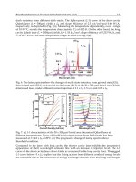
Fig. 15. (a) InGaAlAs RTD-EAM transmission spectrum in the wavelength range 1500 nm to
1580 nm, with the applied voltage as a parameter. (b) Modulator response as function of the
dc bias voltage when driven by 3 GHz rf signals, with injected amplitude as a parameter.
RTD-EAM high frequency optical characterisation employed a microwave synthesized
signal generator with a maximum output of +20 dBm and an upper frequency limit of 26
GHz (Figueiredo, 2000). Figure 16(a) shows the modulation depth as function of the light
wavelength induced by the transition between the two PDC regions produced by a square
signal with peak-to-peak voltage slight higher than
ΔV
VP
~ 0.8 V. The devices were dc biased
in the valley region in order to minimize thermal effects and avoid self-oscillations.
Modulation depths up to 28 dB were measured on devices with active areas around 800
μ
m
2
, more than 10 dB superior to the values observed on the AlGaAs/GaAs devices. The
modulator response up to 26 GHz driving signals for two power values is shown in Fig. 16(b).
Fig. 16. (a) Modulation depth as function of the wavelength. (b) Spectrum of the 26 GHz
photo-detected signal at the modulator driving power of -20 dBm and +7.7 dBm.
Advances in Optical and Photonic Devices
190
The photo-detected power increases more than 10 dB when the driving rf power rises from -
20 dBm to +7.7 dBm, an indication the device is capable to achieve modulation extinction
ratios higher than 10 dB induced by low power driving signals, less than 10mW, as the
consequence of the built-in electrical amplifier. The RTD intrinsic amplifier effect reduces
substantially the rf power required for modulation. This on-chip amplification can eliminate
the need of an external rf amplifier which is usually required to drive EAMs (Wakita et al.,
1998).
3.4 RTD-OW operation as photo-detector at 1550 nm
Light-wave receivers contain photo-detecting devices that convert the light-wave carrier
modulation into an electrical signal that needs to be amplified before processing to recover
the information signal (Liu, 1996)(Einarsson, 1996). The amplifying circuitry can be the
system main penalty in terms of cost and power. We are currently investigating a receiver
based on the RTD-OW to take advantage of the RTD intrinsic built-in amplifier.
Because in the RTD-OW the light interaction length is much longer than in conventional
RTDs, the RTD-OW will produce substantial inter-band absorption, giving rise to a
responsivitygain superior to the one obtained with conventional photo-detectors (Moise et
al., 1995). The RTD-OW photo-detection characterization employed light from a Tunics
tunable laser diode capable to be directly modulated up to 1 GHz and operate in the mode
locked regime at 5 GHz. Figure 17(a) presents the rf power capture level when light
modulated at 1 GHz was end-fire coupled to the waveguide. The RTD-OW responsitivity-
gain increases with the transition from peak to valley voltage, V
p
and V
v
, by more than 15
dB. Figure 17(b) shows the photo-detected rf power as function of wavelength for dc bias on
the peak and on the valley. Photo-detection of mode locked light at 5 GHz showed similar
performance.
Fig. 17. (a) RTD-OW I –V characteristic and rf power produced due 1550 nm optical signals
modulated at 1 GHz. (b) Rf power produced optical signals modulated at 1 GHz as function
of wavelength, at DC biased on the peak and on the valley.
When dc biased in the NDC region the RTD-OW self-oscillations lock to the injected light
subcarrier, producing electrical signals that emulate the optical subcarrier. We are currently
investigating the synchronization between optical subcarriers and RTD-OW free-running
oscillations to transfer the information bearing signals such as Phase Shifted Keyed signals from the
optical to the rf wireless domain without the need of an external amplifier (Romeira
a
et al., 2009).
Resonant Tunnelling Optoelectronic Circuits
191
4. RTD laser diode integration
A light-wave transmitter comprises a driving circuit and a LED or a laser diode which
converts the supplied electrical signal containing the information into a light-wave signal.
Novel alternatives to traditional laser diode transistor-driver circuits have been proposed
based on the integration of a DBQW with semiconductor light sources, since the DBQW
layers fit well with the epitaxial layers that make up semiconductor light sources.
Furthermore, since the RTD can act as a voltage controlled switch, low voltage digital
signals can be employed to switch the RTD between on and off states. It is expected the light
sources high-speed modulation characteristics will improve significantly. In what follows
we make a brief description of the first monolithic integration of a RTD with an optical
communication laser operating at 1500 nm, and give a detailed report on recent advances on
the hybrid integrated version operating at 1550 nm optical windows.
4.1 RTD-LD monolithic integration
The first integration of a DBQW-RTD and an optical communication laser operating at
around 1500 nm was reported by (Slight & Ironside, 2007). The device consisted of a vertical
integration of a DBQW on an InGaAs/InGaAlAs multiple quantum well laser structure.
Such integration is straightforward as the RTD section requires only the growth of four to
six extra epilayers above a laser structure grown on p–type InP substrate, allowing the RTD
to be implemented on the laser junction n–type region. The DBQW was made of a 5 nm
InGaAs well and 2 nm AlAs barriers. The devices fabricated were ridge waveguides with
the DBQW situated in the ridge between the laser section and the n–type contact, Fig. 18(a).
A detailed description of device structure and fabrication can be found in (Slight et al.,
2006). The RTD-LD current-voltage characteristic emulates the RTD non-linear I – V curve,
hysteresis and bistability (Slight & Ironside, 2007). Figure 18(b) shows a typical RTD-LD
optical-voltage characteristic at 130 K, where a hysteresis window is clearly seen; bistable
operation was also observed (Slight et al., 2006). The results demonstrate the feasibility of
monolithically integrated RTDs with LDs. In order to achieve room temperature operation a
new wafer was designed and device fabrication will start soon. Further investigation of the
monolithic RTD-LD will include high-frequency operation characterization.
Fig. 18. (a) Cross section schematic of the ridge waveguide RTD-LD. (b) optical-voltage
(P –V) characteristic at 130 K, clearly showing bistability and hysteresis.
Advances in Optical and Photonic Devices
192
4.2 RTD-LD hybrid circuit
Once demonstrated the bistable operation of monolithically integrated RTD-LDs the work
concentrated on the hybrid integrated circuit (HIC) versions using components similar to
the targeted monolithic integrated device. Although without the monolithic expected
superior performance, laboratory hybrid RTD-LDs are easy and much less costly to
implement, allowing to study both components behaviour separately. The first HICs
combined an InGaAs RTD and a commercial prototype laser diode (Slight & Ironside, 2007).
The In- GaAs RTD used was fabricated from RTD epi-material originally used in the work
described in section 3; the laser diode was a 5
μ
m ridge wide waveguide designed for
continuous-wave (CW) emission at around 980 nm. The RTD and LD were attached to a
small copper block using electrically conductive silver epoxy resin, and connected in series
through 25
μ
m diameter gold wire bonding, as schematically represented in Fig. 19(a). Also
shown are LD and RTD-LD experimental and PSPICE simulated I –V characteristics, Fig.
19(b) (Slight & Ironside, 2007). The PSPICE code used can be found in (Slight & Ironside,
2007).
The RTD reduces significantly the laser driving circuits’ complexity by taking advantage of
its high nonlinear I –V characteristic, with the NDC region providing electrical gain to the
circuit. The RTD features make possible to operate the RTD-LD as an autonomous OVCO,
where the running frequency is fine tuned by the dc bias voltage. Light modulation due to
relaxation oscillations at 5 MHz was observed with optical power on/off or extinction ratio
up to 31 dB. Moreover, because of RTD bistability the RTD-LD optical output is also
bistable, as shown in Fig. 19(c), a feature of particularly convenience for non-return to zero
(NZR) digital modulation.
Fig. 19. (a) Illustration of the RTD-LD module. (b) LD and RTD-LD I – V characteristics. (c)
Optical power versus voltage (P – V) characteristic showing bistability and a 410 mV wide
hysteresis loop. Dashed lines show the PSPICE simulations.
To increase the relaxation oscillations free-running frequency the hybrid circuit was
redesigned. InGaAlAs RTD-OW devices with areas around 1000
μ
m
2
were used together
with commercial prototype ridge waveguide laser dies designed for CW operation with
emission at around 1550 nm with 5 mW average output power, bandwidth of 20 GHz and
threshold current I
th
around 6 mA. The new circuits layouts were mounted directly onto the
surface of printed circuit boards (PCBs) containing a 50 Ω copper microstrip transmission
line laminated onto the non-conductive PCB substrate. These new improvements on the
hybrid RTD-LD circuits lead to some significant breakthroughs: (i) the use of commercial
communications laser diodes operating at 1550 nm; (ii) the oscillation frequency went up to
for more than two orders of magnitude by solving the instabilities associated to the dc bias
circuitry; (iii) demonstration of operation as an autonomous relaxation oscillator in the GHz-
range, controlled by voltage; (iv) observation of new operation capabilities induced by
injected periodic and phase modulated signals.
Resonant Tunnelling Optoelectronic Circuits
193
In the improved circuits the RTD and LD components were attached directly onto the PCBs
using silver epoxy resin and bond wires where used to connect the RTD emitter contact to
LD, and the RTD collector contact to the 50
Ω copper microstrip line, as shown in Fig. 20(a).
A parallel resistor-capacitor shunt was incorporated as close as possible to the RTD-LD
components to reduce the spurious oscillations and to act as a short circuit for the rf signals
generated by the RTD-LD. The circuit shunt component values were typically 5
Ω and 3.3
nF. The dc bias and rf injected signals were applied via a wideband bias-T through the
resistor-capacitor shunt that also acts as the circuit input port. The circuit electrical output
port was defined by the PCB ground plane and the microstrip line, and corresponds to the
RTD-LD series terminals as shown in Fig. 20(a). The laser optical output was coupled to a
lensed fibre before photo-detection. The light coupling efficiency was estimated from the
laser mode profile and single mode fiber characteristics to be around 10 per cent. In Fig.
20(b) are presented the typical I-V characteristics of the LD (with the threshold current inset)
and of two RTD-LD circuits, I and II, measured without the shunt resistorcapacitor. RTD-LD
circuits I and II analysed here have similar PCB layout designs and LD and shunt
components. The RTDs used in circuit I and II have approximately the same current peaks,
I
p
, but different valley currents, I
v
, and thus different peak-to-valley current ratios. RTD-LD
II was designed to have a lower bond wire length connection between RTD and LD
components, which increased its oscillation frequency operation, as discussed below. In
both cases I
th
< I
v
, which meant that when dc biased in the NDC region, the lasers were
working well above threshold current.
Au
Printed Circuit Board
Microstrip line
n
p
rf
rf
out
out
Optical
out
RTD
RTD
LD
LD
dc + rf
dc + rf
(a)
(b)
shunt
components
Fig. 20. (a) Layout of the improved hybrid RTD-LD circuit. (b) Current-voltage characteristic
of the laser diode and two RTD-LD circuits, showing the RTD NDC is preserved by the
RTDLD module.
The RTD-LD circuit of Fig. 20(a) can be represented by circuit electrical layout of Fig. 21(a).
When dc biased in or close to the NDC region the laser diode is operating well above the
threshold current the laser is well represented simple by its differential resistance. Because
its capacitance is much larger than the RTD’s, the RTD-LD module equivalent capacitance
corresponded to the RTD intrinsic capacitance. This approximation seems reasonable since
changing the laser diode did not alter the circuit free-running frequency whenever the
lengths of the bond wires used to connect the RTD to the LD were identical. Indeed, the
circuit of Fig. 21(a) behaves at rf frequencies like an RL circuit connected to the RTD small
signal equivalent circuit (a voltage dependent current source F(V) in parallel with the RTD-
LD capacitance, as discussed in section 2.2). Its electric behaviour under external
perturbation can be studied numerically using the small signal equivalent circuit shown in
Fig. 21(b). The lumped LCR components of Fig. 21(b) represents the microstrip transmission
line and wire bond equivalent inductance, the RTD intrinsic capacitance and the devices
equivalent series resistance, respectively.
Advances in Optical and Photonic Devices
194
rf out
dc + rf
50
50
Optical
out
Microstrip
Microstrip
line
line
PCB
PCB
50
50
RTD
RTD
LD
LD
V
(a)
(b)
V
dc
C
F
(
V
)
V
R
+ V sin(2 f t)
ac in
L
V
I
I
NDC
RTD
RTD
shunt
components
Fig. 21. (a) Electrical schematic of the RTD-LD circuit where V represents the electrical
output taken across the RTD-LD. (b) RTD-LD small-signal equivalent lumped circuit. V
ac
sin(2
π
f
in
t) represents an ac injected driving signal.
The maximum operating free-running frequency of circuit RTD-LD I was around 640 MHz,
whereas for RTD-LD II the maximum observed free-running frequency was 2.15 GHz (the
maximum obtained with the hybrid circuits presented here). The RTD-LD II higher running
frequency was mainly due to the smaller inductance achieved with this circuit layout due to
the shortening of bond wires length used to connect the RTD to the LD, roughly from 5 mm
to less than 2 mm that corresponded to a reduction of the equivalent inductance value from
approximately 8 nH to around 1.5 nH. In both circuits the estimated capacitance C was 3 pF.
These values when used in the electrical circuit model, Eq. 8, lead to theoretical maximum
relaxation oscillation frequencies, given by 1/2
π
L
C , around 1.03 GHz and 2.37 GHz,
respectively.
4.3 RTD-LD optoelectronic model
When dc biased in the NDC region, the circuit of Fig. 20(a) behaves as a classic negative-
resistance oscillator (Van der Pol, 1927). Since the circuit of Fig. 21(b) is similar to the circuit
of Fig 4, apart from the injected ac driving signal V
ac
sin(2
π
f
in
t), we applied the same
procedure, obtaining a second-order differential equation (see section 2.2), commonly
referred as one of the generalized forced nonlinear Liénard systems (Romeira et al.,
2008)(Figueiredo, 1970):
() ()= sin(2 )
ac in
VHVVGV V ft
π
++
(13)
where G(V) is a nonlinear force and H(V)
V
is the damping factor (see section 2.2).
To describe the RTD-LD optoelectronic behaviour we coupled equation 13 to the laser diode
single mode rate equations that governs the interrelationship between carrier density and
photon density. Assuming the laser oscillates in a single mode and the population inversion
is homogeneous, the laser rate equations for photon density S and injected carrier density N
are:
00
=()
1
n
IN S
NgNN
qS
ϑ
τε
−− −
+
(14)
00
=( )
1
p
n
SSN
SgNN
S
β
ε
ττ
−++
+
(15)
Resonant Tunnelling Optoelectronic Circuits
195
where I is the total current through the laser diode given by generalized Liénard’s system,
Eq. 13, plus the dc bias current; q is the electron charge,
ϑ
is the laser active region volume,
τ
n
and
τ
p
are the spontaneous electron and photon lifetimes, respectively;
β
is the
spontaneous emission factor; g
0
is the gain coefficient; N
0
is the minimum electron density
required to obtain a positive gain and
ε
is the value for the nonlinear gain compression
factor. The numerical analysis employed typical parameters of semiconductor laser diodes,
as described in (Slight et al., 2008)(Romeira et al., 2008). The coupled system of equations 13-
15 has been successfully used to predict the experimental behaviour of RTD-LD electrical
and optical outputs.
4.4 RTD-LD optoelectronic voltage controlled oscillator
It is well known that a single-port device that has a negative differential conductance in a
portion of its operating range may be used as the basis of a bistable or multistable circuit, and
can also be used to form astable circuits (relaxation oscillators), monostable circuits (single-
pulse generators), and sine-wave generators (Brown et al., 1997). A simple way to implement a
RTD oscillator is to couple a RTD dc biased in the NDC to a resonant tank circuit or a resonant
cavity that provides frequency stability (the coupling location in the cavity can serve to
partially match its impedance to that of the RTD). Such oscillator corresponds to a relaxation
oscillator system since it operates by sequential transitions between unstable states. The RTD-
LD circuit of Fig. 20(a), whose circuit schematic is represented in Fig. 21 with the small signal
equivalent circuit, operates as a relaxation oscillator when dc biased in the NDC region. The
circuit free-running frequency is determined primarily by the round trip time of the ac
feedback loop (effective length of equivalent transmission line from the shunt resistor-
capacitor to the RTDLD module), in combination with the RTD and the LD parasitics (mainly
the inductance from the wire bonding).
The RTD successive switching events (relaxation oscillations) produce sharp current pulses
that modulate the laser output yielding sharp optical pulses at the relaxation oscillation
fundamental frequency (free-running frequency). Typical RTD-LD self-sustained oscillation
voltage output and photodetect optical waveforms are shown in Fig. 22. Figure 22(a) shows
RTD-LD I voltage output waveform at free-running frequency around 600 MHz; Fig. 22(b)
presents the photo-detected laser optical output modulated by the current relaxation
oscillations with an on/off superior to 20 dB.
The pulsed nature of the photo-detected laser optical output shown in Fig. 22 confirms the
capacitive character of the current induced by the RTD switching (described in detail in
(Brown et al., 1997)). The full width at half maximum (FWHM) of the photo-detected pulses
is approximately 200 ps but this measurement is limited by the temporal acquisition
resolution of the oscilloscope. Figure 23 shows rf spectra of the electrical and optical outputs
of RTD-LD circuits I and II of Fig. 20(b), both dc biased close to the valley region. Figure
23(a) confirms the pulse nature of the current relaxation oscillations with a high harmonic
content up to 12
th
harmonic being measured.
Tuning the dc bias across the NDC region changes the RTD impedance and as consequence
tunes the relaxation oscillation frequency making the circuit operate as a voltage controlled
oscillator (VCO). Since the current relaxation oscillation waveforms flow through the laser
diode, the circuit optical output emulates the current oscillations. The laser output shows
the same repetitive switching and harmonic content of the relaxation oscillation current
waveforms, making the RTD-LD circuit operate as an optoelectronic voltage controlled
oscillator (OVCO). That is, the RTD-LD biased on the NDC region produces electrical and
Advances in Optical and Photonic Devices
196
Fig. 22. RTD-LD I relaxation oscillation (a) electrical and (b) photo-detected optical output
waveforms at around 600 MHz.
Fig. 23. Electrical and photo-detected optical spectra of free-running oscillations at 600 MHz
(a) and 2.1 GHz (b), circuits I and II, respectively.
optical oscillatory signals whose frequency is controlled by the bias voltage quiescent point.
Figure 24 shows the frequency response to dc voltage sweep across the NDC region of
circuits RTD-LD I and II, whose I –V characteristics are presented in Fig. 20(b).
The oscillation frequency of circuit I changed with the dc voltage from around 500 MHz to
640 MHz, that is, RTD-LD I had a tuning range around 140 MHz, whereas the circuit II
oscillate from 1.97 GHz to 2.15 GHz, i.e., RTD-LD II had a tuning range around 180 MHz.
Although the dc voltage tuning of circuit I was larger, the tuning sensitivity/tuning
performance expressed in tuning range per voltage range was higher for circuit II. In the
RTD-LD oscillators analyzed, we found that a linear deviation characteristic is attained
considering only voltages close to the peak voltage. The voltage tuning range of circuit I, Fig
24(a), is much larger than the circuit II, Fig. 24(b), as expected from higher PVVR measured
in the I –V characteristic. Frequency tuning ranges up to 450 MHz were observed in RTD-LD
circuits having NDC widths and I – V characteristics identical to RTD-LD I. Generally
speaking, to have a wide dc operating range and therefore large tunability, a wide negative
conductance region (large difference between the peak and valley voltage) is required.
Resonant Tunnelling Optoelectronic Circuits
197
Fig. 24. RTD-LD I (a) and RTD-LD II (b) experimental and simulated frequency tuning
responses to voltage sweeping across the NDC regions.
The RTD-LD optoelectronic voltage controlled oscillator is a simple way to convert fast, short
electrical pulses with low timing jitter and phase noise, into fast, sharp optical pulses.
4.5 Phase-locking
The injection-locking of an electrical oscillator was first described by (Van Der Pol, 1927),
and the first locking bandwidth equation for electrically injection-locked oscillators was
developed by (Adler, 1946), with a model based on a vacuum tube transistor. The most
comprehensive theoretical review of injection-locking solid-state oscillators was given by
(Kurokawa, 1973). Most of the characteristic and properties identified by the above authors
can be observed with RTD-LD circuits which are much simpler oscillator configuration.
When externally perturbed the RTD-LD circuit behaves as a non-autonomous oscillator
(Romeira
b
et al. 2009), being a practical demonstration of nonlinear systems theory
extensively developed over the last decades (Pikovsky et al., 2001).
Throughout the work, we observed that under appropriated bias and injection conditions
the RTD-LD circuit relaxation oscillations lock to low-power injected signals that take over
the oscillations, controlling the laser diode output characteristics. To investigate these
locking characteristics periodic external signals at microwave frequencies were injected into
the circuit. The analysis included the effects of the frequency, signal power level, and
injected signal modulation formats. Phase-locking with significant noise reduction to low
power signals (below -30 dBm) at frequencies around the circuits’ natural frequencies are
observed. Figure 25(a) presents rf spectra of photo-detected laser optical outputs when the
circuit was free-runing at 600 MHz and when phase-locked to -25 dBm power rf signal also
at 600 MHz. The single side band (SSB) phase noise measurement showed the oscillation
noise at 10 kHz offset was reduced by about 35 dB due to the phase-locking. For the
conditions of Fig. 25(a) the locking range was 1.8 MHz. The frequency locking range
increases as the injected power rises, as shown in Fig. 25(b). This behavior is well described
by the optoelectronic model presented previously and is represented by the red zone of Fig.
25(b), known as Arnold tongue. Arnold tongues correspond to synchronization regions
were locking occurs between two competing frequencies (Pikovsky et al., 2001). When the
injected signal frequency becomes out of the oscillator locking range, the circuit generate
mixing products of the injected signal and free-running oscillations.
Advances in Optical and Photonic Devices
198
Since the phase of a signal plays an important role in communications, particularly wireless
communication, and in the theory of synchronisation, we investigated the effect of phase
modulation in the RTD-LD outputs. Figure 25(c) shows circuit response to an injected 600
MHz carrier phase modulated with 1 MHz frequency sub-carrier with phase shift
π
and
3
π
/2. As the sub-carrier frequency was varied from 100 kHz up to 2 MHz, the laser output
followed the phase modulation of the sine-wave signal subcarrier.
Fig. 25. (a) Rf spectra of photo-detected laser output in free-running mode and when phase-
locked to -25 dBm injected signal at 600 MHz frequency. (b) Frequency locking range as
function of the injected power. The dotted points are experimental data and the red area
(Arnold tongue) was numerically obtained. (c) Rf spectra of photo-detected laser output
when phase-locking to a phase modulated 600 MHz sine-wave carrier signal.
The observed phase-locking converts phase differences on shifts in the laser output
modulating its intensity. This behaviour can be applied to implement phase shift keying
(PSK) digital modulation, which is employed in numerous digital communication systems.
The phase-locking capabilities of RTD-LD based relaxation oscillators can also be used for
error free timing extraction in optoelectronic circuits.
4.6 Frequency division operation
When the injected signal frequency is out of the oscillator locking range the circuit generates
mixing products of the injected signal and free-running oscillations, producing either/ both
harmonic and sub-harmonic phase-locking. To investigate the mixing capability of the
circuit we analysed numerically the behaviour of the circuit over a range of frequencies to
obtain the laser optical output bifurcation diagram of Fig. 26. A bifurcation diagram shows
the amplitude peaks heights of output photon density oscillations, S, as a function of the
normalized excitation frequency f
in
/ f
0
, where f
0
is the free running oscillation frequency. The
simulation results show that when the frequency of the injected signal, f
in
, is successively
increased, a stable period–n, n = 1, 2, is obtained, followed by an unlocked region, then a
stable period–(n +1), a new unlocked region and so on (Figueiredo et al., 2008)(Pikovsky et
al., 2001). This phenomenon is known as period-adding, where windows of consecutive
regions showing frequency division are separated by zones of unlocked, even chaotic,
signals. The frequency division regions were obtained experimentally and calculated
numerically dc biasing the RTD-LD circuit on the NDC region and varying the frequency of
the injected signal from 0.1 GHz to 3 GHz, with drive amplitudes as low as 100 mV.
Frequency division regions for constant amplitudes were observed following the period-
Resonant Tunnelling Optoelectronic Circuits
199
adding sequence at up to frequency division by 6. In Fig. 26(a) the period-adding is clearly
distinguished in a sequence of unlocked (dots) and periodic (branch regions) oscillations, as
observed experimentally. Figure 26(b) presents an experimental example of frequency
division by 2 when a 0.9 GHz sine-wave was injected.
Fig. 26. (a) Calculated bifurcation diagram for V
ac
= 150 mV up to frequency division by 6.
(b) Photo-detected laser output showing frequency division by 2 when a signal with f
in
= 0.9
GHz was injected into an RTD-LD free-running oscillating at around 0.5 GHz.
Since the sub-harmonic windows appear in limited frequency regions, the RTD-LD circuit can
be regarded as an optoelectronic dynamic frequency divider with a selectable dividing ratio.
4.7 Aperiodic and chaotic operation
Electro-optical and all-optical solutions for complex chaos generation have attracted
considerable attention in the last decade due to their potential applications in optical chaos
communications (Argyris et al., 2005). The use of chaotic carriers allows steganography at
the physical layer, which can substantially improve the security of software encryption
techniques. The frequency bands corresponding to period multiplication, indicated in Fig.
26(a), are separated by frequency regions where the circuit generates aperiodic signals -
chaotic or quasi-periodic output - a direct result from the mixing between free-running
oscillation and external injected frequencies (Romeira et al. 2010). An important
characteristic of a chaotic signal is its sensitivity to initial conditions. Figure 27 shows an
example of a transition to chaos observed in the RTD-LD circuit optical output. The optical
waveform presented in Fig. 27(a) is characterized by a series of aperiodic acute peaks
(spikes) changing chaotically. Another important characteristic of chaos is demonstrated in
the corresponding power spectrum of the time series. Figure 27(b) shows a continuous and
broadband spectrum resembling a noisy process with a few dominant frequencies
appearing, in this case the rf injected frequency. The results of Fig. 27 are also confirmed
numerically by calculating the circuit Lyapunov exponents (Romeira et al., 2001).
This RTD-LD mode of operation provides a simply way to generate and convert electrical
chaotic signals into optical sub-carriers that can be transmitted by conventional optical
Advances in Optical and Photonic Devices
200
channels. Moreover, the circuit allows direct addition of the message to be transmitted and
masked within the chaotic signal.
Fig. 27. Chaotic behaviour in the laser output induced by a driving signal of frequency
1.485 GHz and amplitude 793 mV. Optical waverform (a) and corresponding Fourier
spectrum (b).
5. Conclusion
As discussed, embedding DBQW-RTDs within semiconductor optical waveguides can lead
to the implementation of highly efficient electro-absorption modulators and photo-detectors
operating at optical wavelengths around 900 nm and 1550 nm. The presence of the DBQW
introduces high non-linearities and NDC regions in the semiconductor optical waveguides
current-voltage characteristics, making the electric field distribution across the waveguide
core strongly dependent on the bias voltage, which can be used to modulate guided light
through the Franz-Keldysh electro-absorption effect. When biased on the NDC region the
RTD-OW operates as an optoelectronic voltage controlled oscillator. Electro-absorption
modulation up to 28 dB is achieved with high frequency signals as low as 100 mV. The key
difference between these RTD-OW electro-absorption modulators and conventional p – i – n
electro-absorption modulators is that the RTD-EAM has in essence an integrated electronic
amplifier and therefore requires considerably less switching/driving power. Since, the RTD-
OWs can also work as photo-detectors with built-in amplifiers, recovering the original
transmitted rf signals used to modulated the optical carriers, they can be employed at the
base station to convert information from the optical to the rf domains. We foresee that
optimized devices can have bandwidths up to 60 GHz.
By integrating a DBQW-RTD with a laser diode low-cost microwave-photonic circuits
operating up to 2.15 GHz were implemented. These circuits reduced significantly the
driving circuitry of laser diodes. Several optoelectronic operation modes were observed,
including optoelectronic voltage controlled oscillator (OVCO), phase-locking, frequency
division and generation of aperiodic electrical and optical waveforms. Their simple circuit
layout is appropriated for high functional single chip transmitter platforms due to their non-
linear optoelectronic characteristics, reduced size and low power consumption. We
Resonant Tunnelling Optoelectronic Circuits
201
anticipate that the optimised RTD-LD monolithic integrated versions can operate at much
higher frequencies (tens of Gbits), having several advantages when compared to
conventional devices currently used in lightwave communication systems.
The RTD-OW and RTD-LD operation as optoelectronic voltage controlled oscillators can be
used to simplify significantly clock generation and clock extraction circuits. Due to the
nonlinear response to applied voltage the RTD based circuits can work as short optical pulse
generators with high repetition rates. At the same time, their integration with other
functional devices can be used to encode generated optical pulses. The combination of RTD-
OW and RTD-LD functions on a single circuit can be used to incorporate simultaneously rf
subcarrier signals into optical carriers and optical subcarrier signals into rf carriers. This is
possible due the following simultaneously capabilities: modulation, photo-detection and
intrinsic amplification. Thus, the RTD-OW and RTD-LD circuits offer the possibility of
implementing very simple microwave/photonics interfaces of cellular network terminal
base stations based on radio-over-fiber systems.
Since next generation wireless access picocellular networks will be based on large numbers
of short range cells with each office in a building with its own cells and base stations, the
RTD based optoelectronic devices offer low cost single chip solutions as microwave/optical
interfaces capable of electrical-to-optical conversion of microwave signals into optical
subcarriers, taking advantage of the NDC and phase-locking properties of RTD devices. The
photo-detecting capabilities allows recovery of the original transmitted rf signals used to
modulated the optical carriers sent from the office terminal station to each base station via
optical fibre, converting the information from the optical to the rf domain; light generation
function is used to transfer the wireless received information bearing signals from the rf
domain to optical domain which is then sent from the base stations to the office terminal
station via optical fibre.
6. Acknowledgment
Bruno Romeira and José Figueiredo acknowledge the support of the Centro de
Electrónica, Optoelectrónica e Telecomunicações, Portugal. This work was also supported
in part by the Fundação para a Ciência e a Tecnologia, Portugal, through the grants
PRAXIS XXI/BD/2871/94 and SFRH/BD/43433/2008, by the Fundação Calouste
Gulbenkian, Portugal, and by Research Networks - Treaty of Windsor Programme
2008/09-U32, Portugal. The authors would like to thank W. Meredith of Compound
Semiconductor Technologies Global, Ltd. for providing the laser diodes, and Liquan
Wang and Edward Wasige by the fruitful discussions and PCB layout design in the RTD-
LD work.
7. References
Adler, R. (1946). A study of locking phenomena in oscillators. Proc. I.R.E.Waves Electrons,
351- 357
Alkeev, N. V.; Lyubchenko, V. E.; Ironside, C. N.; Figueiredo, J. M. L. & Stanley C. R. (2000)
Super high-frequency characteristics of optical modulators on the basis of
Advances in Optical and Photonic Devices
202
InGaAlAs resonance-tunnel heterostructures. J. Commun. Technol. Electron., Vol. 45,
No. 8, Aug. 2000, 911–914
Argyris, A.; Syvridis, D.; Larger, L.; Annovazzi-Lodi, V.; Colet, P.; Fisher, I.; Garcia-Ojalvo,
J.; Mirasso, C.; Pesquera, L.; Shore, K. A. (2005). Chaos-based communications
at high bit rates using commercial fibre-optic links. Nature, Vol. 43, Nov. 2005, 343–
346
Bohm, D. (1951). Quantum theory, Prentice-Hall Inc., New Jersey
Böhrer, J.; Krost, A. & Bimberg, D. B. (1993). Composition dependence of band gap and type
of lineup in InGaAlAs/InP heterostructures. Appl. Phys. Lett., Vol. 63, No. 14, Oct.
1993, 1918
Brown, E. R.; McMahon, O. B.; Mahoney, L. J. & Molvar, K. M. (1996). SPICE model
of the resonant-tunneling diode. Electronics Lett., Vol. 32, No. 10, May 1996,
938–940
Brown, E. R. & Parker C. D. (1996). Resonant tunnel diodes as submillimetre-wave sources.
Phil. Trans. R. Soc. Lon. A, Vol. 354 , No. 1717, Oct. 1996, 2365–2381
Brown, E. R.; Parker, C. D.; Verghese, S. & Geis, M. W. (1997). Resonant-tunneling
transmission-line relaxation oscillator. Appl. Phys. Lett., Vol. 70, No. 21, May 1997,
2787
Capasso, F.; Mohammed, K. & Cho A. Y. (1986). Resonant tunneling through double
barriers, perpendicular quantum transport phenomena in superlattices, and
their device applications. IEEE J. Quantum Electron., Vol. 22, No. 9, Sep. 1986, 1853–
1869
Chang, L. L.; Esaki, L. & Tsu, R. (1974). Resonant tunneling in semiconductor double
barriers. Appl. Phys. Lett., Vol, 24, No. 12, Jun. 1974, 593
Chen, L.; Kapre, R. M.; Hu, K. & Madhukar, A. (1991). High-contrast optically bistable
optoelectronic switch based on InGaAs/GaAs (100) asymmetric Fabry-Perot
modulator, detector, and resonant tunneling diode. Appl. Phys. Lett., Vol. 59, No. 13,
Sep. 1991, 1523–1525
Chuang, S. L. (1995). Physics of optoelectronic devices JohnWiley & Sons Inc., New York
Davies, J. H. (1998). The physics of low-dimensional semiconductors: an introduction, Cambridge
University Press, Cambridge.
Einarsson, G. (1996). Principles of lightwave communications, John Wiley & Sons, New
York
England, P.; Golub, J. E.; Florez, L. T. & Harbison, J. P. (1991). Optical switching in a
resonant tunneling structure. Appl. Phys. Lett., Vol.58, No. 9, Mar. 1991,
887–889
Figueiredo, R. (1970). Existence and Uniqueness results for Liénards equation. IEEE
Transactions on Circuit Theory, Vol. CT-17, No. 3, Jun. 1970, 313–321
Figueiredo, J. M. L.; Boyd, A. R.; Stanley, C. R.; Ironside, C. N.; McMeekin, S. G. & Leite, A.
M. P. (1999). Optical modulation at around 1550 nm in an InGaAlAs optical
waveguide containing an InGaAs/AlAs resonant tunneling diode. Appl. Phys.Letts,
Vol. 75, No. 22, Nov. 1999, 3443–3445
Resonant Tunnelling Optoelectronic Circuits
203
Figueiredo, J. M. L. (2000). Optoelectronic Properties of Resonant Tunneling Diodes, PhD Thesis,
Universidade do Porto, Porto
Figueiredo, J.M.L.; Stanley C.R. & Ironside C.N. (2001). Electric Field Switching in a
Resonant Tunneling Diode Electroabsorption Modulator. IEEE Journal of Quantum
Electronics, Vol. 37, No. 12, Dec. 2001, 1547–1552
Figueiredo, J. M. L.; Ironside C. N. & Stanley. C. R.; (2002). Ultralow voltage resonant
tunneling diode electroabsorption modulator. Journal of Modern Optics, Vol. 49, No.
5, Apr. 2002, 939–945
Figueiredo, J. M. L.; Romeira, B.; Slight, T. J.;Wang, L.;Wasige E. & Ironside C. N. (2008).
Selfoscillation and period adding from a resonant tunnelling diode laser diode
circuit. Electronics Letters, Vol. 44, No. 14, Jul. 2008, 876–878
Gravé, I.; Kan, S. C.; Griffel, G.; Wu, S. W.; Sa’ar, A. & Yariv, A. (1991). Monolithic
integration of a resonant tunneling diode and a quantum well semiconductor laser.
Appl. Phys. Lett. Vol. 58, No. 2, Jan. 1991, 110-112
Huang, C. Y.; Morris, J. E. & Su, Y. K. (1997). Generalized formula for the stability and
instability criteria of current-voltage characteristics measurements in the negative
differential conductance region of a resonant tunneling diode. J. Appl. Phys., Vol. 82,
No. 5, Sep 1997, 2690
Iogansen, L. V. (1964). The possibility of resonance transmission of electrons in crystals
through a system of barriers. Soviet Physics JETP, Vol. 18, 146
Katz, A. (1992). Indium phosphide and related materials: processing, technology, and
devices, Artech House, London
Kawamura, Y.; Wakita, K.; Asai, H. & Oe, K. (1987). Optically bistable operation in InGaAs-
InAlAs MQW laser diodes using resonant tunnelling effect. Electron. Lett., Vol. 23,
No. 14, 719–721
Kawamura, Y.; Wakita, K. & Mikami, O. (1988). InGaAs/InAlAs bistable multiple quantum
well lasers with large on/off ratio using the resonant tunneling effect. Appl. Phys.
Lett., Vol.53, No. 16, Oct. 1986, 1462–1464
Kawamura, Y.; Asai, H.; Matsuo, S. & Amaro, C. (1992). InGaAs-InAlAs multiple quantum
well optical bistable devices using the resonant tunneling effect. IEEE J. Quantum
Electron., Vol. 28, No. 1, Jan. 1992, 308-314
Kawamura, Y.; Asai, H. & Iwamura, H. (1994). Fabrication of resonant-tunnelling optical
bistable laser diodes. Electron. Lett., Vol. 30, No. 3, Feb. 1994. 225–227
Keldysh, L. V. (1958). The effect of a strong electric field on the optical properties of
insulating crystals. Sov. Phys. JETP, Vol. 34, 788
Kidner, C.; Mehdi, I.; East, J. R. & Haddad, G. I. (1990). Power and stability limitations of
resonant tunneling diodes. IEEE Trans. Microwave Theory and Techniq., Vol. 38, No.
7, Jul 1990, 864–872
Kurokawa, K. (1973). Injection locking of microwave solid-state oscillators. Proc. IEEE, Vol.
61, No. 10, Oct. 1973, 1386–1410
Lann, A. F.; Grumann, E.; Gabai, A.; Golub, J. E.; & England, P. (1993). Phase locking
between light pulses and a resonant tunneling diode oscillator. Appl. Phys. Lett.,
Vol. 62, No. 1, Jn. 1993, 13-15
Advances in Optical and Photonic Devices
204
Liu, M. M K. (1996). Principles and applications of optical communications, Irwin Book,
London.
Mazumder, P.; Kulkarni, S.; Bhattacharya, M.; Sun, J. P. & Haddad, G. I. (1998). Digital
circuit applications of resonant tunneling devices. Proceedings of the IEEE, Vol. 86,
No. 4, Apr. 1998, 664–686
McMeekin, S. G.; Taylor, M. R. S.; V¨ogele, B.; Stanley, C. R. & Ironside, C. N. (1994). Franz-
Keldysh effect in an optical waveguide containing a resonant tunneling diode,
Appl. Phys. Lett., Vol 65, No. 9, Aug. 1994, 1076-1078
Mizuta, H. & Tanoue, T. (1995). The physics and applications of resonant tunneling diodes,
Cambridge University Press, Cambridge
Moise, T. S.; Kao, Y C.; Garrett, L. D. & Campbell, J. C. (1995). Optically switched resonant
tunneling diodes. Appl. Phys. Lett., Vol. 66, No. 9, Feb. 1995, 1104–1106
Moise, T. S.; Kao, Y C.; Goldsmith, C. L.; Schow, C. L. & Campbell, J. C. (1997). High-speed
resonant-tunneling photodetectors with low-switching energy. IEEE Photonics
Technol. Lett., Vol. 9, No. 6, Jun. 1997, 803–805
Park, T. J.; Lee, Y. K.; Kwon, S. K.; Kwon,J. H. & Jang, J. (2006). Resonant tunneling diode
made of organic semiconductor superlattice. Appl. Phys. Lett. Vol. 89, No. 15, Oct.
2006, 151114
Pikovsky, A.; Rosenblum, M. & Kurths J. (2001). Synchronization: A universal concept in
nonlinear sciences, Cambridge Univ. Press,Cambridge
Romeira, B.; Figueiredo, J. M. L.; Slight, T. J.; Wang, L.; Wasige, E.; Ironside C. N.;
Quintana, J. M. & Avedillo, M. J. (2008). Synchronisation and chaos in a laser diode
driven by a resonant tunneling diode. IET Optoelectronics, Vol. 2, No. 6, Dec. 2008,
211-215
Romeira
a
, B.; Figueiredo, J. M. L.; Slight, T. J.; Wang, L.; Wasige, E. & Ironside C. N. (2009)
Wireless/Photonics Interfaces Based on Resonant Tunneling Diode Optoelectronic
Oscillators, Conference on Lasers and Electro-Optics (CLEO)/The International Quantum
Electronics Conference (IQEC), paper CTuT4, Baltimore, Maryland, USA, May 31-
June 5, 2009, OSA Technical Digest (CD) Optical Society of America
Romeira
b
, B.; Figueiredo, J. M. L.; Slight, T. J.; Wang, L.; Wasige, E.; Ironside, C. N.; Kelly, A.
E. & Green, R. (2009). Nonlinear Dynamics of Resonant Tunneling Optoelectronic
Circuits for Wireless/Optical Interfaces. IEEE J. Quantum Electron., Vol. 45, No. 11,
Nov. 2009, 1436-1445)
Romeira, B.; Figueiredo, J. M. L.; Ironside, C. N. & Slight, T. J. (2010). Chaotic Dynamics in
Resonant Tunneling Optoelectronic Voltage Controlled Oscillators. to be published
in IEEE Photonics Technol. Lett. DOI: 10.1109/LPT.2009.2034129
Ryu, S. Y.; Jo, S. J.; Kim, C. S.; Choi, S. H.; Noh, J. H.; Baik, H. K.; Jeong, H. S.; Han, D.W.
Song, S. Y. & Lee, K. S. (2007). Transparent organic light-emitting diodes using
resonant tunneling double barrier structures. Appl. Phys. Lett. Vol. 91, No. 9, Aug.
2007, 093515
Sakata, H.; Utaka, K. & Matsushima, Y. (1995). Diferent types of optoelectronic bistabilities
in resonant-tunnelling triangular-barrier optoelectronic switch (R-TOPS). Electron.
Lett., Vol. 31, No. 13,Jun 1995, 1098–1099
Resonant Tunnelling Optoelectronic Circuits
205
Sauer, M.; Kobyakov, A. & George, J. (2007). Radio over fiber for picocellular network
architectures. J. Lightw. Technol., Vol. 25, No. 11, Nov. 2007, 3301–3320
Sano, K.; Murata, K.; Akeyoshi, T.; Shimizu, N.; Otsuji, T.; Yamamoto, M.; Ishibashi T. &
Sano, E. (1998). Ultra-fast optoelectronic circuit using resonant tunnelling diodes
and uni-travelling-carrier photodiode. Electron. Lett., Vol 34, No. 2, Jan. 1998, 215–
217
Schulman, J. N.; De Los Santos, H. J. & Chow, D. H. (1996). Physics-based RTD
current-voltage equation. IEEE Electron Device Lett., Vol. 17, No. 5. May 1996, 220–
223
Slight, T. J.; Ironside, C. N.; Stanley, C. R.; Hopkinson, M. & Farmer, C. D. (2006). Integration
of a resonant tunneling diode and an optical communications laser. IEEE Photonics
Technology Letters, Vol. 18, No. 14, Jul. 2006, 1518–1520
Slight, T. J. (2006). Integration of a Resonant Tunnelling Diode and an Optical Communications
Laser, PhD Thesis, University of Glasgow, Glasgow
Slight, T. J. & Ironside, C. N. (2007). Investigation into the integration of a resonant
tunneling diode and an optical communications laser: model and experiment. IEEE
J. Quant. Elec. Vol. 43, No. 7, Jul 2007, 580–587
Slight, T. J.; Romeira, B.; Wang, L.; Figueiredo, J. M. L.; Wasige E., & Ironside, C. N. (2008). A
Liénard oscillator resonant tunnelling diode-laser diode hybrid integrated circuit:
model an experiment. IEEE J. Quantum Electron., vol. 44, no. 12, Dec. 2008, 1158–
1163
Sollner, T. C. L. G.; Goodhue, W. D.; Tannenwald, P. E.; Parker, C. D. & Peck, D. D. (1983).
Resonant tunneling through quantum wells at frequencies up to 2.5 THz. Appl.
Phys. Lett., Vol. 43, No. 3, Sep. 1983, 588–590
Sun, J. P.; Haddad, G. I.; Mazumder, P. & Schulman, J. N. (1998). Resonant tunneling
diodes: models and properties. Proceedings of the IEEE, Vol. 86, No. 4, Apr. 1998,
641–660
Suzuki, S.; Teranishi, A.; Hinata, K.; Asada, M.; Sugiyama H. & Yokoyama H. (2009).
Fundamental Oscillation of up to 831 GHz in GaInAs/AlAs Resonant Tunneling
Diode. Appl. Phys. Express, Vol. 2, Apr. 2009, 054501
Tsu, R. & Esaki, L. (1973). Tunneling in a finite superlattice. Appl. Phys. Lett., Vol. 22, No. 11,
Jun. 1973, 562–564
Wada, O. (1994). Optoelectronic integration: physics, technology and applications, Kluwer
Academic Publishers, Massachusetts
Wakita, K. (1998). Semiconductor optical modulators, Kluwer Academic Publishers,
London
Weisbuch, C. & Vinter, B. (1991). Quantum semiconductor structures: fundamentals and
applications, Academic Press Inc., London
Van Der Pol, (1927). Forced Oscillator in a circuit with nonlinear resistance. Phil. Mag. Vol. 3,
65–80
Van Hoof, C.; Genoe, J.; Mertens, R.; Borghs, G. & Goovaerts, E. (1992). Electroluminescence
from bipolar resonant tunneling diodes. Appl. Phys. Lett., Vol. 60, No. 1, Jan 1992,
77–79
Advances in Optical and Photonic Devices
206
Van Hoof, C.; Genoe, J.; Raymond, S. & Borghs, G. (1993). Giant optical bistable behavior
using triple-barrier resonant tunnelling light-emitting diodes. Appl. Phys. Lett., Vol.
63, No. 17, Oct. 1993, 2390–2392
Zheng, T.; Choy,W. C. H. & Sun, Y. (2009). Hybrid Nanoparticle/Organic Devices with
Strong Resonant Tunneling Behaviors. Advanced Functional Materials, Vol. 19, No.
16, Jul. 2009, 2648-2653
11
Integrated-Optic Circuits for
Recognition of Photonic Routing Labels
Nobuo Goto, Hitoshi Hiura, Yoshihiro Makimoto and Shin-ichiro Yanagiya
The University of Tokushima
Japan
1. Introduction
An optical fiber provides enormous capacity of more than tens terabits per second for
transmission in photonic networks, whereas packet processing in network nodes will
become a bottleneck for large-capacity networking. For realization of large-capacity and
high-speed photonic networks, fast optical processing without conversion to electric signal
is preferable (Seo et al., 1996; Blumenthal et al., 2000).
Photonic routing has been attracting much interest to overcome the bottleneck of routing
function in high-speed networks. In particular, photonic label routing network is expected
to provide fast routing of packets at high-bit rate with simple processing. So far, various
methods for optical label encoding and decoding have been studied (Kitayama et al., 2000;
Goto & Miyazaki, 2005). As one of the nature of light, phase of coherent light has been
effectively used in various optical systems, where the interference behavior between
multiple signals can be easily used. Using this feature, label recognition techniques have
been investigated for photonic routers based upon optical code correlation. However, most
of the proposed systems cannot recognize all the binary codes because only the codes that
provide enough discrimination between auto-correlation and cross-correlation can be
recognized. In addition, in most systems, each optical integrated circuit recognizes only one
label (Wada et al., 1999; Takiguchi et al., 2002). Therefore, it is necessary to prepare multiple
correlators at each node in order to recognize all the routing labels. On the contrary, for
processing of multiple labels, Moriwaki et al. (Moriwaki et al., 2005) and Cincotti (Cincotti,
2004) proposed label recognition systems where self-routing architecture was employed for
phase-shift-keying (PSK) labels. On the other hand, Glesk et al. reported a demonstration of
optical multiple label recognition for on-off keying (OOK) codes at 250Gbit/s using a self-
routing scheme (Glesk et al., 1997). The self-routing of label data stream for label recognition
is one of promising methods in label decoding system.
Hiura & Goto proposed a label recognition system for OOK labels (Hiura et al, 2005; Hiura
et al, 2007a). Although the proposed system can recognize all the binary-code labels, the
system requires many optical switches controlled by optical signals. A similar system was
also reported by Kurumida et al. (Kurumida et al., 2006). On the other hand, Hiura et al. also
proposed an all-optical passive label recognition system for all the binary codes in binary
PSK (BPSK) format (Hiura et al., 2006; Hiura et al., 2007b). The label recognition system
consists of a tree-structure connection of passive waveguide components named as
Advances in Optical and Photonic Devices
208
asymmetric X-junction coupler (Izutsu et al., 1982; Burns & Milton, 1975; Burns & Milton,
1980), and time gates. The asymmetric X-junction coupler provides a function of wave
coupling according to the phase relation between the two incident waves. The asymmetric
X-junction coupler has an advantage that the wave coupling behavior does not depend on
wavelength because the wave coupling utilizes an adiabatic wave coupling along the X-
junction. This feature cannot be obtained with other devices such as 3-dB directional
couplers or multi-mode interference (MMI) couplers.
The number of represented labels in PSK format can be increased by employing multiple
phases such as four phases as quadri-PSK (QPSK). Optical circuits for detecting QPSK signal
have been investigated for receivers in communication systems (Renaudier et al., 2008).
When QPSK labels are introduced in label routing system, optical processing of the QPSK
labels is required. We have proposed a label recognition circuit for QPSK labels (Makimoto
et al., 2008; Makimoto et al, 2009a). The circuit consists of the asymmetric X-junction
couplers, Y-junctions and 3-dB directional couplers.
In this article, we describe the principle of label recognition for BPSK and QPSK coded
labels in the self-routing scheme. The operation of the label recognition with optical
integrated circuits are confirmed by finite-difference beam propagation method (FD-BPM).
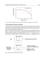
2. Photonic label router
Optical labels are used as a routing information in photonic label switching network as
shown in Fig.1. A label is attached to the incident packet at an edge router. The label is
used to forward the packet to another edge router which is connected to the destination of
the packet. At a node, routing switches are controlled according to the label information by
referring to a routing table. At first, the label has to be analyzed to find the destination
information. Therefore, the label has to be inspected whether the label matches with any of
the all labels at the routers.
If the network is designed in a hierarchical structure so that a router at a node in a sub-
network is required to find only the packets destined to the sub-network, it is not required
for the router to resolve all the labels. Therefore, it depends on the network architecture and
routing protocol whether all the labels have to be resolved or only a part of the labels are
required to be resolved.
Core
Router
Switch
Edge
Router
Edge
Router
IP packet
Label
I
1
I
n
O
m
O
1
Core
Router
Switch
Label Routing Network
Fig. 1. Label routing network.
Integrated-Optic Circuits for Recognition of Photonic Routing Labels
209
3. Optical label and its recognition
Various methods have been investigated to represent routing label information as optical
signals, which include coding of the labels in time-domain, in spectral domain, and in their
combination. Here we consider time sequential coded pulse train in BPSK and QPSK
modulation formats. In these pulses encoded in phase, a reference signal is required to
identify their absolute phase. Although differential PSK formats can be alternatives that do
not require the reference phase signal, we introduce a reference pulse in advance of the
pulses representing an address to identify general PSK address as shown in Fig.2. The
electric field of the optical pulse train of an (N+1)-bit label is written as
,)()(
0
)(
0
∑
=
Δ−
Δ−=
N
i
titj
j
label
eetitftE
i
ω
φ
(1)
where f
0
(t) denotes the envelope of a pulse with the angular frequency ω, the phase
φ
i
and
the pulse period
Δ
t. j is the imaginary symbol of
1−=j
. The phase is 0 or π in BPSK
labels and 0, π/2, π or 3π/2 in QPSK labels. The phase
φ
0
is assumed to be 0 as the reference
pulse, named as identifying (ID) bit in our self-routing label recognition systems. The other
phases
φ
i
, i=1,…, N, represent the address.
t
Δ t
ID bit
Address bits
φ
1
φ
2
φ
N
φ
0
t
0
t
1
t
2
t
N
Fig. 2. Label structure in PSK format.
Label
Output ports
1
2
3
M
t
Label
recognition
system
Input port
Fig. 3. Label recognition system.
The label recognition is performed by forwarding the ID-bit pulse to an output port
corresponding to the destination of the address as shown in Fig.3. The number of the output
ports M corresponds to the number of all the coded address, that is, M=2
N
and 4
N
for BPSK
and QPSK codes, respectively. Since all the bits of the label arrive sequentially, we employ a
processing circuit to extend all the bits in parallel at a specific time as shown in Fig.4.
Equally-divided pulse trains are sent to the input ports of the label recognition circuit
through delay elements. The incident electric field of the optical signal to input port I
k
,
k=1,…,N+1, is delayed by (k-1)
Δ
t as given by
Advances in Optical and Photonic Devices
210
.))1((
1
1
)(
0
])1([
0
)(
∑
=
Δ−+−
Δ−+−
+
=
N
i
tkitj
j
k
label
eetkitf
N
tE
i
ω
φ
(2)
At time t
c
, all the (N+1)-bit pulses simultaneously enter to the input ports.
Label
pulse
train
Input
ports
Output
ports
Delay line
(
Ν
−1)Δt
NΔt
Δt
φ
0
φ
1
φ
N
I
N
φ
0
φ
1
φ
N
φ
0
φ
1
φ
N
I
N+1
I
1
O
1
O
2
O
M
I
s
Label
recognition
circuit
t
c
t
t
c-1
t
c+1
…
…
Fig. 4. Label recognition with serial-to-parallel conversion as a pre-processing.
Figure 5 shows the principle of label recognition by self-routing manner. Each bit of the
address represents the number of M
0
=2 and 4 for BPSK and QPSK, respectively. The nth-
stage circuit module forwards the ID bit pulse to the output port corresponding to the nth
address bit by using the nth address bit pulse as the control signal. Consequently, the ID bit
pulse appears at the destination port among the M=M
0
N
output ports in the Nth-stage.
ID bit
1st address bit
2nd address bit
Nth address bit
Forward ID bit according to
address bit by interference
O
1
O
2
O
M
1
M
0
Fig. 5. Tree-structure circuit for label recognition by self-routing manner.
4. Basic devices for recognition circuits
Proposed label recognition circuits consist of passive waveguide devices shown in Fig.6. A
3-dB directional coupler shown in (a) is used to couple the optical incident waves into two
output waves. The electric field of the input and output waves, E
in
(i)
and E
out
(i)
, i=1,2, are
related, by eliminating the common phase shift along the propagation, as
⎟
⎟
⎠
⎞
⎜
⎜
⎝
⎛
⎟
⎟
⎠
⎞
⎜
⎜
⎝
⎛
−
−
=
⎟
⎟
⎠
⎞
⎜
⎜
⎝
⎛
)2(
)1(
)2(
)1(
1
1
2
1
in
in
out
out
E
E
j
j
E
E
. (3)
When an optical wave is incident in only one of the waveguide, the wave is equally divided.
The output fields, however, have a phase difference of π/2. A Y-junction shown in (b) also
divides an optical input wave equally into two output ports as expressed by
Integrated-Optic Circuits for Recognition of Photonic Routing Labels
211
E
in
(1)
E
in
(2)
E
out
(1)
E
out
(2)
3-dB coupling
E
in
E
out
(1)
E
out
(2)
(a) (b)
E
in
E
in
ref
E
out
E
out
ref
Δ
φ
E
in
(1)
E
in
(2)
E
out
(1)
E
out
(2)
θ
(c) (d)
Fig. 6. Basic passive elements for label recognition circuits.
.
1
1
2
1
)2(
)1(
in
out
out
E
E
E
⎟
⎟
⎠
⎞
⎜
⎜
⎝
⎛
=
⎟
⎟
⎠
⎞
⎜
⎜
⎝
⎛
(4)
The two output waves have the same phase. A phase shifter shown in (c) shifts the phase
with regard to the reference waveguide. The input-output relation is given by
.
10
0
⎟
⎟
⎠
⎞
⎜
⎜
⎝
⎛
⎟
⎟
⎠
⎞
⎜
⎜
⎝
⎛
=
⎟
⎟
⎠
⎞
⎜
⎜
⎝
⎛
Δ
ref
in
in
j
ref
out
out
E
E
e
E
E
φ
(5)
An asymmetric X-junction coupler shown in (d) is the device whose input and output are a
symmetric Y-junction and an asymmetric Y-junction, respectively (Izutsu et al., 1982). When
two waves are incident in phase, the output is obtained only at the wider-waveguide port.
On the contrary, when two waves are incident in opposite phase, the output is at the
narrower waveguide. This input-output relation is given by
.
11
11
2
1
)2(
)1(
)2(
)1(
⎟
⎟
⎠
⎞
⎜
⎜
⎝
⎛
⎟
⎟
⎠
⎞
⎜
⎜
⎝
⎛
−
=
⎟
⎟
⎠
⎞
⎜
⎜
⎝
⎛
in
in
out
out
E
E
E
E
(6)
It is noted that the output fields have a phase difference of π. The angle
θ
and the waveguide
asymmetry have to be properly designed to realize the ideal routing characteristics. The
phenomenon of optical coupling along an asymmetric Y-branch is evaluated by the coupled
mode theory (Burns & Milton, 1975; Burns & Milton, 1980). A parameter
Ψ
to characterize
the coupling phenomenon is defined by
,
4/)(
22
snw
nw
nNN
NN
−+
−
=Ψ
θ
(7)
where n
s
is the refractive index of the cladding region, N
w
and N
n
are the effective indices of
the wide and narrow waveguides, respectively,
θ
is the branching angle. The ideal function
as given by eq.(6) is expected to be realized in the asymmetric X-junction coupler when
Ψ
>
0.44.
Advances in Optical and Photonic Devices
212
5. BPSK label recognition
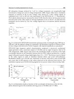
The asymmetric X-junction coupler has a function to discriminate the phase of the incident
wave in BPSK format. A cascaded connection of the asymmetric X-junction couplers in a
tree-structure shown in Fig. 7 can identify two-bit addresses. The symbol X
ij
denotes an
asymmetric X-junction coupler at the ith stage. Each of the waveguides numbered by 3 and
4 corresponds to the wider and the narrower waveguide, respectively. The input and output
fields are related as
(1)
2
(1)
(2)
2
(2)
(3)
2
(3)
(4)
2
11
11
,
11
11
out
in
out
in
out
in
out
E
E
E
E
E
E
E
α
α
α
α
⎛⎞ −
⎛⎞
⎛⎞
⎜⎟
⎜⎟
−
⎜⎟
⎜⎟
⎜⎟
=
⎜⎟
⎜⎟
⎜⎟
⎜⎟
⎜⎟
⎜⎟
⎝⎠
⎜⎟
−−
⎝⎠
⎝⎠
(7)
where
α
2
is an amplification coefficient of the amplifier placed at input port I
3
. We consider
two cases having different value of
α
2
. First we consider the case of
α
2
=1. When optical two-
bit BPSK pulse train is incident, the normalized intensity of the pulse trains appears from
four output ports as shown in Fig.8. The maximum output is found at time t
c
, and four
11
X
21
X
22
X
amplification: α
2
I
2
I
1
I
3
O
2
O
1
O
3
O
4
Power divider
2
13
4
2
13
4
2
13
4
(1)
in
E
(2)
in
E
(3)
in
E
(1)
out
E
(2)
out
E
(3)
out
E
(4)
out
E
11
X
21
X
22
X
amplification: α
2
I
2
I
1
I
3
O
2
O
1
O
3
O
4
Power divider
2
13
4
2
13
4
2
13
4
(1)
in
E
(2)
in
E
(3)
in
E
(1)
out
E
(2)
out
E
(3)
out
E
(4)
out
E
ij
X
2
13
4
2
13
4
ij
X
2
13
4
2
13
4
Fig. 7. BPSK label recognition circuit for label length three.
0
0.5
1
1.5
2
2.5
12345
Time sequence
N ormalized Intensity
O1
O2
O3
O4
t
c-2
t
c-1
t
c
t
c+1
t
c+2
0
0.5
1
1.5
2
2.5
12345
Time sequence
Normalized Intensity
O1
O2
O3
O4
t
c-2
t
c-1
t
c
t
c+1
t
c+2
(a) address 00 (b) address 0π
0
0.5
1
1.5
2
2.5
12345
Time sequence
N ormalized Inten sity
O1
O2
O3
O4
t
c-2
t
c-1
t
c
t
c+1
t
c+2
0
0.5
1
1.5
2
2.5
12345
Time Sequence
Normalized Intensity
O1
O2
O3
O4
t
c-2
t
c-1
t
c
t
c+1
t
c+2
(c) address π0 (d) address ππ
Fig. 8. Time sequential output intensity for four addresses with the circuit of α
2
=1.
Integrated-Optic Circuits for Recognition of Photonic Routing Labels
213
different addresses have the peak intensity at their corresponding output port. The contrast
ratio of the peak intensity to the second largest intensity at time t
c
is 9. Since the inputs to the
second asymmetric X-junction couplers, X
2j
, j=1,2, have different intensities, the output from
the port whose paired port has the maximum intensity has a non-zero output.
Next, we consider the case of
α
2
=2. The pulse train from four output ports appear as shown
in Fig.9. In this case, the input intensities to the X-junction coupler that has the maximum
output are equal, and no output at the paired port. The contrast ratio of the maximum
intensity to the second intensity at time t
c
is decreased to 4.
0
1
2
3
4
5
12345
Time sequence
N orm alized Inten s ity
O1
O2
O3
O4
t
c-2
t
c-1
t
c
t
c+1
t
c+2
0
1
2
3
4
5
12345
Time sequence
Normalized Intensity
O1
O2
O3
O4
t
c-2
t
c-1
t
c
t
c+1
t
c+2
(a) address 00 (b) address 0π
0
1
2
3
4
5
12345
Time sequence
N orm alized Intensity
O1
O2
O3
O4
t
c-2
t
c-1
t
c
t
c+1
t
c+2
0
1
2
3
4
5
12345
Time Sequence
N o rmalized Intensity
O1
O2
O3
O4
t
c-2
t
c-1
t
c
t
c+1
t
c+2
(c) address π0 (d) address ππ
Fig. 9. Time sequential output intensity for four labels with the circuit of α
2
=2.
11
X
21
X
22
X
31
X
32
X
33
X
34
X
α
2
amplification:α
3
I
2
I
1
I
3
I
4
O
1
O
2
O
3
O
4
O
5
O
6
O
7
O
8
2
13
4
2
13
4
2
13
4
2
13
4
2
13
4
2
13
4
2
13
4
(1)
in
E
(2)
in
E
(3)
in
E
(4)
in
E
(1)
out
E
(2)
out
E
(3)
out
E
(4)
out
E
(5)
out
E
(6)
out
E
(7)
out
E
(8)
out
E
11
X
21
X
22
X
31
X
32
X
33
X
34
X
α
2
amplification:α
3
I
2
I
1
I
3
I
4
O
1
O
2
O
3
O
4
O
5
O
6
O
7
O
8
2
13
4
2
13
4
2
13
4
2
13
4
2
13
4
2
13
4
2
13
4
(1)
in
E
(2)
in
E
(3)
in
E
(4)
in
E
(1)
out
E
(2)
out
E
(3)
out
E
(4)
out
E
(5)
out
E
(6)
out
E
(7)
out
E
(8)
out
E
Fig. 10. BPSK label recognition circuit for label length four.
The circuit shown in Fig.7 can be scaled up for label length four as shown in Fig.10. The
pulse train coupled in the input port I
4
is amplified by a factor
α
3
and divided into four
pulse trains for the third-stage X-junction couplers. The contrast ratio of the maximum
output intensity to the second largest intensity is decreased as shown in Fig.11. It is found
that for the case of
α
m
=1, m=2,…, N-1, 7-bit addresses can be recognized with the contrast
ratio of 2.5[dB]. On the contrary, for the case of
α
m
=2
m-1
, even 4-bit addresses are difficult to