Advances in optical and photonic devices Part 3 pptx
Bạn đang xem bản rút gọn của tài liệu. Xem và tải ngay bản đầy đủ của tài liệu tại đây (2.72 MB, 20 trang )
Photonic Quantum Ring Laser of Whispering Cave Mode
31
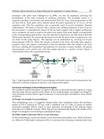
As shown in the schematic Fig. 16, a tapered single mode fiber tip about 300nm in diameter
was made by chemical etching for the photon collection, and a step motor generates relative
motions of the tip against probed PQR laser device. The collected photon signal goes
through single photon counting module, photon counter, and computer.
Fig. 16. A schematic diagram of home-built 2D/3D single photon scanning system.
Figure 17 shows some 2D scan results over a scan area of 60x60 um square, where, on the
surface of the PQR, Fig. 17(a) exhibits that the emission pattern of the PQR beam is Laguerre
Gaussian for the case of a mesa PQR, and Fig. 17(b) shows another Laguerre Gaussian
pattern for the case of hole PQRs.
Fig. 17. (a) Lagurre Gaussian beam of the mesa PQR (b) Lagurre Gaussian beam of the hole
PQR
8. Fabrication of micro collimators for PQR beam guiding
Laser printers with mechanically rotating polygon mirrors have been used widely in offices,
whereas new LED printers, quiet and all-electronic drive circuitry with no moving parts,
begin to replace them. However, the LED, being a spontaneous emission device with some
disadvantages as stated earlier, can further be replaced by an efficient laser like the PQR
laser diode with extremely low threshold currents and
T -dependent thermally stable
spectral properties which are good for fast, high density array applications. Moreover,
typical LED printers use selfoc-lens arrays (SLAs) to concentrate and guide individual light,
Advances in Optical and Photonic Devices
32
but the expensive SLA technology is complicated. We note that the PQR laser with the micro
collimator (MC) for non-parallel to parallel beam guiding described previously may replace
the LED + SLA technology. In order to find such a possibility, we will now describe several
fundamental features of the PQR laser such as the beam shape and propagation behaviors,
MC-guided PQR beams, beam divergence, and high power capabilities.
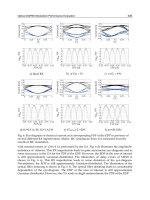
For beam divergence studies, Fig. 18(a) represents a PQR emission pattern observed from a
device of a 48um diameter which is rather close to the Lambertian emission pattern of a
conventional LED. However noting that the Gaussian beam is characterized by the spot size
and divergence angle θ, recent 3D PQR beam profile studies of 15um PQR lasers also show
possibilities of controlling the beam divergence to the narrower ranges, for example a
divergence angle of θ = 2 x 6.3 degree as shown in Fig. 18(b). This analysis results from the
3D scans made at 30, 60 and 90 um heights respectively as shown in Figs. 18(c),(d) and (e),
where divergence points are determined as half maximum intensity points. We find from
the 3D scans that the initial beam profile of Laguerre Gaussian is evolving to Gaussian as a
function of scan height. The beam shapes are nearly Gaussian at 30um height and perfectly
Gaussian at 60um height, which gives rise to a cross-over from Laguerre Gaussian to
Gaussian at around 40~50um height. In our divergence analysis we may regard the PQR
ring as a Bessel beam formed at the rim of the PQR device surface from an imaginative point
light at the origin located deep below the device surface.
Fig. 18. (a) Lambertian profile of a PQR (b) Divergence angle of a PQR (c) (d) and (e)
represent beam scans taken at different heights, 0, 30, and 60 um
For practical system applications of light sources one often has to find how to control, or
focus and guide, the laser beam. Therefore we now turn to an active beam control method
employing convex and concave MCs for focusing and guiding the PQR light through lens
media and free space. The convex and concave lenses of the MC are designed and fabricated
as shown in Figs. 19(a) and (b).
Photonic Quantum Ring Laser of Whispering Cave Mode
33
A master lens array is made by a photoresist (PR) reflow method, and the PR microlens
array is transferred to a polydimethyl-siloxane (PDMS) master by a casting method. Finally,
the PDMS is spin-coated again on the PDMS master, whose details are described (O'Neill &
Sheridan, 2002). Fig.19(a) are SEM images of the final micro lens arrays fabricated to be
17um in diameter and 10um in height for the convex lenses (top) and 36um in diameter for
the concave lenses (bottom).
Fig. 19(c) represents a series of CCD snap shots taken at various distances from the PQR
laser surface where the microlens set on the fifth spot happens to be absent. The snap shots
vividly shows that the propagating Gaussian beam is guided to the point of minimum spot
at 160um distance and reconstructs the original PQR laser image at around 400um distance.
The fact that the missing 5
th
spot is not affected by any possible neighbor’s diffraction ghost
means that the PQR beam behaves as a Bessel beam.
Fig. 19. (a) Convex and concave lens arrays. (b) Outline of beam guiding optics. (c) CCD
snap shots taken at different distances.
9. Design and SEM images of flower PQR laser
We now describe the design and fabrication of the new flower PQR laser for output power
enhanced about 5 times the power expected from regular circular PQR lasers of the same
size, where 4, 8, and 12 –petal flower designs, combining concave and convex whispering
cave modes, result in the increased overall quantum wire length of the emitting PQR within
the same device area.
As shown earlier in Fig. 13(a), the PQR region emitted first and much brighter than the
central LED emission region, which means a very high emission efficiency of the PQR laser.
We however note that the emission region is occupied mostly by the central LED emission
Advances in Optical and Photonic Devices
34
in this case. That is the reason why we make use of the flower design in enhancing the PQR
light output power since the increase of the PQR region by sacrificing the central LED area
are achieved with more number of petals in a fixed diameter mesa. When the current
density is the same, the more the number of petals, say the more the area of peripheral PQR
region, the more the flower PQR laser intensity. We however note that the total length of
peripheral PQR curves is to be smaller than the critical length for GaAs PQRs,
corresponding to the device perimeter of a critical diameter (
φ
= ~50 μm), so that the
quantum ring whispering cave mode begins to disappear (Kwon et al., 2006).
The photonic quantum ring (PQR) laser is an attractive candidate for high-density “laser”
displays, given the unique operating characteristics attendant on its quantum-wire-like nature,
such as extremely low threshold currents and thermally stable spectra in the typical operating-
temperature range. When vertical mesa cavities are made of λ/4
Al0.92Ga0.08As/Al0.16Ga0.84As distributed Bragg reflector (DBR) structures added below
and above an active region of multi-quantum wells (QWs) of 7nm thick GaAs each separated
by 8nm thick barriers of Al0.3Ga0.7As, emitting at 850nm. Moreover, we have observed
unusual convex WCMs from reverse-mesa (=hole)-type micro-resonators, whose WCMs we
interpreted with respect to gain-guiding and photonic quantum corral effects. We now re-
stress that the light output power observed enhances roughly in proportion to the number of
petals of the flower PQR laser, up to the point where the total PQR perimeter reached a critical
length corresponding to that of a circular PQR laser of about 50 μm diameter.
Circular and 4, 8, and 12-petal flower PQR lasers of the same overall diameter (Φ = 20 μm)
for example are designed and fabricated. We can calculate the various multi-petal PQR
perimeters’ total lengths corresponding to the respective quantum wire lengths of Rayleigh
band. The circular PQR of Φ = 20 μm has a peripheral PQR length of about 63 μm. When the
number of petals, in the same overall diameter (Φ = 20 μm) of flower, is 8, the total
peripheral PQR length is about 84 μm, and when the number is 12 then the total length is
about 115 μm. The increased number of petals is more or less proportional to the growth of
flower PQR output power, which is roughly proportional to the total peripheral PQR length.
The SEM image of a 12-petal flower PQR laser is shown as an example in Fig. 20. Mesas 4.2
Fig. 20. SEM images of 12-petal flower PQRs (a) without hole (b) with hole (c) and (d) show
illuminant PQRs at different injection levels.
Photonic Quantum Ring Laser of Whispering Cave Mode
35
μm high were etched by chemically assisted ion beam etching (CAIBE) with a photoresist
mask. The smoothness of the side wall is an important factor in minimizing the spectral
linewidth of PQR lasers. For side wall smoothness and highly anisotropic etching, we tilt
and rotate the substrate in the CAIBE chamber during the etching process while adding
BCl3 gas to facilitate Al2O3 removal in addition to an Ar/Cl2 gas mixture. Full details are
given in a reference (Kim et al., 2004)
10. Fabrication of high power flower PQR laser
Fig. 21 shows emission images of various flower PQR lasers of Φ = 20 μm. For comparison,
we simultaneously fabricated a circular mesa PQR laser of Φ = 18 μm. A tremendous
intensity build-up occurred after increasing injection currents, so that appropriate neutral
density filters had to be used for intensity attenuation. PQR lasing occurs along the
perimeter of the active disk called the Rayleigh bandwidth, 0.63 μm width for Φ = 20 μm
(Ahn et al., 1999), while LED emission occurs in the central bulk region of the PQR mesa. A
threshold of 28 μm (= 11 A/cm2), observed through ring pattern schemes as shown in Fig.
21, is apparently smaller than the threshold range around 20 – 30 A/cm2 as estimated via
usual extrapolation schemes, where the convex TIR effect of ‘hole’ PQR portions is involved
in addition to the ‘soft lasing turn-on’ behavior (Kim et al., 2009).
25A/cm
2
50A/cm
2
100A/cm
2
T=1.0% T=1.0% T=1.0%
T=1.0% T=1.0% T=1.0%
T=1.0% T=1.0% T=0.63%
Circle 18um, I=15uA
PQR emission
LED emission
25A/cm
2
50A/cm
2
100A/cm
2
25A/cm
2
50A/cm
2
100A/cm
2
12-petals, I
th
=28uA
11A/cm
2
T=100%
25A/cm
2
50A/cm
2
100A/cm
2
T=1.0% T=1.0% T=1.0%
T=1.0% T=1.0% T=1.0%
T=1.0% T=1.0% T=0.63%
Circle 18um, I=15uA
PQR emission
LED emission
25A/cm
2
50A/cm
2
100A/cm
2
25A/cm
2
50A/cm
2
100A/cm
2
12-petals, I
th
=28uA
11A/cm
2
T=100%
Fig. 21. Various emission patterns of 4-, 8-, 12- petal flower PQRs
As mentioned earlier, the flower design enhances the PQR light output power, thanks to the
increase of the effective PQR region, while reducing the central LED area by means of a
greater number of petals in a given diameter mesa. When the current density is the same,
the greater the number of petals (the larger the area of the peripheral PQR region), the
higher the flower PQR laser intensity. We can describe the light intensity as a function of the
number of petals. For the devices with 20um width, the optical output power increased
when the number of petals increased (Fig. 22). As the number of petals increased, the length
of peripheral PQR region is larger so that the region occupied by the PQR emission in the
whole emission region increased, leading to the final increase of the optical output power.
Advances in Optical and Photonic Devices
36
Fig. 22. Optical output power comparison (
φ
= 20 μm)
11. Panel-less TV display scheme with RGB PQR lasers
Today the market of display is dominated by LCD and PDP flat panel display (FPD) TVs,
while expensive wider panels become too heavy to handle. The PQR laser is an attractive
candidate for next generation display. We are currently developing a panel-less laser image
chip for TV display using addressable PQR (photonic quantum ring) laser-pixels. For high
brightness, wide-picture and full-color high definition TVs, we can design optimized
projection systems involving RGB PQR laser array strategies, and lens optics for image
magnification and projection similar to a light engine, where the RGB PQR display module
will be the basic building block filling up the 2D/3D lattice of infinitely expansible TV display.
Fig. 23 is a schematic diagram of a beam combination demonstrator for RGB color display.
Fig. 23. A beam combination example
In the case of red beam, for example, the schematic may involve 1 or 2 lenses for beam
guiding, resulting in an instantaneous frame of red beam scan implemented through an
arrangement of optical components as shown Fig. 24. The blue and green beam combination
structures are under development.
Photonic Quantum Ring Laser of Whispering Cave Mode
37
Fig. 24. (a) Red beam optics outlined. (b) Red letter image (c) Experimental set up of the
optical components
12. Conclusions
We have presented studies of 3D WCM of PQRs. The 3D WCM laser is surface-normal
dominant and has no in-plane resonance while the 2D WGM laser is in-plane dominant.
Also the 3D WCM’s major polarization state favors such a strong carrier-photon coupling
that the powerful transient coupling generates PQRs, i.e., a photonic quantum corral effect.
This gives rise to the low threshold currents and thermally stable spectra, important for easy
optical mega-pixel (‘Omega’) chip fabrications which will be useful for next generation TV
display. We have also presented Gaussian beam properties and guiding work of the PQR
laser.
13. References
Ahn, J. C. et al., Photonic quantum ring, Phys. Rev. Lett. 82, No.3 pp 536-539 (1999).
Armani, D. K. et al., Optical microcavities, Nature 421, 925 (2003); Min, B. et al., Erbium-
implanted high-Q silica toroidal microcavity laser on a silicon chip, Phys. Rev. A70,
033803 (2004).
Bae, J. et al., Spectrum of three-dimensional photonic quantum-ring microdisk cavities:
comparison between theory and experiment, Opt. Lett. 26, 632 (2003).
Feidhlim, T. & O
’Neill, J., Photoresist reflow method of microlens production Part I,
International Journal for Light and Electron Optics, 113. 391 (2002)
Gehrig ,E. et al., Dynamic filamentation and beam quality of quantum-dot lasers, Appl. Phys.
Lett. 84, 1650 (2004).
Ide, K. et al., LaGuerre–Gaussian Emission Properties of Photonic Quantum Ring Hole-Type
Lasers, IEEE Trans. Nano. 7, 185 (2008).
Advances in Optical and Photonic Devices
38
Kim, D. & Kwon, O., Polarization characteristics of photonic quantum ring laser with three-
dimensional whispering gallery resonances, J. Appl. Phys. 102, 053104(2007).
Kim, J. Y. et al., Fabrication of Photonic Quantum Ring Laser using Chemically Assisted Ion
Beam Etching, J. Vac. Sci. Technol. B. 19, 1334 (2001).
Kim, J. Y. et al., Effect of surface treatment on leakage current of GaAs/AlGaAs laser
microcavitys, Appl. Phys. Lett. 82, 4504 (2003).
Kim, M. et al., Wet etching fabrication of photonic quantum ring laser, J. Appl. Phys. 96, 4742
(2004).
Kim, Y. C. et al., PQR laser can outdo LED, IEEE-NMDC 2006 21-24 (2006), Gyeongju, Korea;
Laser Focus World (March 2008).
Kwon, O. et al., Photonic quantum ring laser of 3D whispering cave mode, Microelectronics
Journal, 40, 570 (2009)
Kwon, O. et al., Hole emitter of photonic quantum ring, Appl. Phys. Lett, Vol. 89, 11108 (2006)
McCall, S. L. et al., Whispering-gallery mode microdisk lasers, Appl. Phys. Lett.60, 289 (1992).
Noeckel, J. & Stone D., Ray and wave chaos in asymmetric resonant optical cavities, Nature
385, 45-47 (1997); Gmachl, C., High-power directional emission from microlasers
with chaotic resonators, Science 280, 1556 (1998).
Park, B. H. et al., Chiral wave propagation manifold of the photonic quantum ring laser,
Appl. Phys. Lett. 81, 580 (2002).
Topinka, M.A. et al., Imaging Coherent Electron Flow, Physics Today 56, 12 (2003).
Wiersig, J. & Hentschel, M., Combining Directional Light Output and Ultralow Loss in
Deformed Microdisks, Phys. Rev. Lett. 100, 033901 (2008)
Yoon, J. H. et al., Single mode photonic quantum ring laser fabricated in hyperboloid drum
shape, J. Appl. Phys. 103, 053103 (2008)
3
A Tunable Semiconductor Lased Based on
Etched Slots Suitable for Monolithic Integration
D. C. Byrne, W. H. Guo, Q. Lu and J. F. Donegan
School of Physics, Trinity College Dublin
Ireland
1. Introduction
Widely tunable semiconductor lasers will play a critical part in future technologies. Tunable
lasers are rapidly replacing fixed wavelength lasers in dense wavelength division
multiplexing DWDM optical communications. The performance specifications of tunable
lasers are the same as fixed wavelength specifications plus additional specifications that
include: wavelength tuning range; wavelength switching speed; and minimum wavelength
spacing. Tunable lasers diodes (TLD) have been used in optical networks for some time now
starting with devices with small wavelength coverage and moving towards full band
coverage.
Wavelength-agile networks are also simplified with tunable lasers. Reconfigurable optical
add–drop multiplexers (ROADMs) and wavelength-based routing enable service providers
to offer differentiated services, meet the ever-increasing demand for bandwidth and deliver
all-optical networking. Tunable lasers are key to addressing this growing need to
reconfigure networks remotely. The use of widely tunable lasers helps maximize existing
network resources. The ability to dynamically provision bandwidth provides the ability to
optimize the network configuration to meet demand. Widely tunable lasers move traffic
from overcrowded channels to unused channels and are becoming essential for the network
architecture.
Future DWDM networks will make more use of wavelength converters to increase network
flexibility. Wavelength converters, such as, optical-electronic-optical (OEO) converters with
the ability to detect a high data rate signal on any input wavelength channel and to convert
to any output wavelength channel, will use tunable lasers. Future uses for tunable lasers
will also include packet based selection of the wavelength on which the packet is to be
transmitted. The tunable laser switching speed for these applications will be of the order of
micro-seconds or longer. They will typically need to be widely tunable, i.e. tunable over a
full C or L band and should be tunable to the 50 GHz channel spacing. In some UDWDM
applications, channel spacing of 25 GHz and eventually as close as 12.5 GHz will be
required.
Tunable lasers will also be used as a means to reduce costs as sparing lasers in wavelength
division multiplexing (WDM) systems. New approaches to data transmission such as
coherent WDM (CoWDM (Healy, Garcia Gunning et al. 2007)) require discrete tuning
between particular wavelength channels on a grid. There is additionally an urgent need to
integrate semiconductor lasers with other optical components such as amplifiers,
Advances in Optical and Photonic Devices
40
modulators and detectors (Coldren 2000; Ward, Robbins et al. 2005; Welch, Kish et al. 2006;
Raring & Coldren 2007) in order to reduce chip cost, system size and complexity. Tunable
lasers are also needed in other important markets such as trace gas detection for
environmental emission motoring (Phelan, Lynch et al. 2005).
Laser operation requires optical feedback which is conventionally obtained in a
semiconductor Fabry-Pérot laser by cleaving the ends of the laser waveguide along either
(011) or (01-1) crystallographic planes to form two semi-reflecting facets. However, due to
the need for cleaving, it is difficult to integrate these lasers with other optical components on
a single chip.
Distributed-Bragg-reflector (DBR) lasers and distributed feedback (DFB) lasers which
employ a series of small refractive-index perturbations to provide feedback, do not rely on
cleaved facets and therefore can be integrated with optical amplifiers and modulators.
However, complex processing with multiple epitaxial growth stages is required for
fabricating these lasers. Another method to obtain feedback is to etch a facet. However, this
approach is limited by difficulties in achieving the smoothness and verticality of the etched
facet particularly for structures based on InP materials.
Previously it was shown that by introducing a shallow slot into the active ridge waveguide
of a laser, the longitudinal modes of the Fabry-Perot (FP) cavity were perturbed according to
the position of the slot with respect to the cleaved facets (Coldren & Koch 1984; Peters &
Cassidy 1991; Corbett & McDonald 1995). By judicious placement of a sequence of low-loss
slots with respect to the facets pre-selected FP modes could be significantly enhanced
leading to robust single frequency lasing with wide temperature stability (John, Dewi et al.
2005; O'Brien & O'Reilly 2005) as well as tuning with fast switching characteristics (Phelan,
Wei-Hua et al. 2008). More recently, we have characterized the properties of slots which are
etched more deeply namely to the depth of, but not through, the core waveguide containing
the quantum wells (Roycroft, Lambkin et al. 2007). In that case, the reflection of each slot is
of the order of ~1% with transmission of ~80% and the slot will strongly perturb the mode
spectrum of the FP cavity by creating sub-cavities. The loss introduced by the presence of
the slot is compensated by gain in the laser. An array of such slots can provide the necessary
reflectivity for the laser operation independent of a cleaved facet where the gain between
the slots compensates for the slot loss producing an active slotted mirror region. Such a
mirror has been used in conjunction with a cleaved facet permitting the integration of a
photodetector with the laser. As the laser output facet is not cleaved this can provide a much
easier integration platform on which complex devices such as Mach-Zehnder modulators
(MZI) and semiconductor optical amplifiers (SOA) can be monolithically integrated with the
laser to reduce chip cost and complexity significantly. In this chapter we demonstrate a
tunable laser with an integrated SOA which is used to both increase and balance the output
optical power of different channels.
2. Background on slot design
In this section a single slotted Fabry-Perot laser diode will be introduced which forms the
basis for our tunable platform. The single slot laser is fabricated by etching into the
waveguide of the FP laser diode as described in (DeChiaro 1991; McDonald & Corbett 1996;
Fessant & Boucher 1998; Klehr, Beister et al. 2001; Lambkin, Percival et al. 2004;
Engelstaedter, Roycroft et al. 2008). The slots act as reflection centres and produce a
modulation of the reflection and transmission spectra dependent on the characteristics of the
A Tunable Semiconductor Lased Based on Etched Slots Suitable for Monolithic Integration
41
slot such as slot position, slot depth to which it is etched and slot width. Even though the
slot is not etched into the active (waveguiding) regions it will still interact with the mode of
the electric field (and magnetic field) of the waveguide as the mode profile is not fully
confined to the active region and will expand into the surrounding cladding regions. The
one-dimensional first order electric field mode profile modelled using the finite difference
time domain (FDTD) technique for a simple laser structure with active region depth of 1 µm,
upper cladding region of 1 µm and lower cladding of 1 µm with active region refractive
index of 3.55 and cladding region refractive index 3.41, which are normal values for an
InGaAsP active region sandwiched between InP cladding regions, are shown below in Fig. 1.
Fig. 1. Mode profile of the fundamental mode and refractive index profile through the laser
structure.
From Fig. 1 the fundamental mode is seen to penetrate into the cladding region so any
perturbation in this area will influence the mode profile of the laser diode.
The scattering matrix method (SMM) is a simple and accurate technique which can be used
to determine the reflection and transmission from slots etched into the laser cavity.
Numerous texts deal with the SMM of which (Buus, Amann et al. 2005) is a good
introduction. Of particular importance in a laser structure is the ability to determine loss
using the SMM method. This is an important advantage of the SMM over that transmission
matrix method (TMM). A F-P laser with one etched slot can be described as three cavities
with different interface reflections and transmissions as described below in Fig 2.
Fig. 2. Schematic description of single slot laser diode.
n
2
n
3
n
2
n
1
n
1
r
4
r
3
r
1
r
2
Front section Slot Back section
t
4
t
3
t
2
t
1
n
2
n
3
n
2
n
1
n
1
r
4
r
3
r
1
r
2
Front section Slot Back section
t
4
t
3
t
2
t
1
Advances in Optical and Photonic Devices
42
In fig. 2, n
i
refers to the effective refractive index in these section of the laser structure, while
r
i
refers to the reflection from the interfaces as shown above. Each section can be described
as a separated cavity and the total reflection and transmission is then found. The back
section amplitude reflection from the left side and right side is described from the SMM as
()
(
)
()
()
12 1
1
21
exp 2
1exp2
bb
bl
bb
tr t i L
rr
rr iL
β
β
−−
=+
−− −
(1)
and
()()
(
)
()
()
21 2
2
21
exp 2
1exp2
bb
br
bb
tr t iL
rr
rr iL
β
β
−− −
=− +
−− −
(2)
respectively where
β
is the complex propagation constant (
β
= β
re
+ iβ
im
) and L
b
is the back
section cavity length. The back section amplitude transmission from the left side is described as
(
)
()
()
12
21
exp
1exp2
bb
bl
bb
tt i L
t
rr iL
β
β
−
=
−− −
(3)
and
t
br
= t
bl
giving a power reflection and transmission is R
bl
= (r
bl
)
2
and T
br
= (t
br
)
2
respectively. The
reflection and transmission of the back section and slot region is found by including the
back section reflection and transmission in the SMM calculation as follows
()
(
)
()
()
3
3
3
3exp 2
1exp2
bl s s
bl sl
bl s s
tr t i L
rr
rr iL
β
β
+
−−
=+
−− −
(4)
and
(
)
()
()
3
3
exp
1exp2
bl b b
bl sl
bl s s
tt i L
t
rr iL
β
β
+
−
=
−− −
(5)
again by a continuation of this method the reflection and transmission amplitudes for the
full laser structure can be determined as
()
(
)
()
()
44
4
4
exp 2
1exp2
bl sl f f
totall
bl sl f f
tr t i L
rr
rr iL
β
β
+
+
−−
=+
−− −
(6)
and
(
)
()
()
4
4
exp
1exp2
bl sl f f
totall
bl sl f f
tt i L
t
rr iL
β
β
+
+
−
=
−− −
(7)
A Tunable Semiconductor Lased Based on Etched Slots Suitable for Monolithic Integration
43
where the reflection and transmission from the right is found in a similar fashion to the total
from the left. The calculated power reflection using an experimentally determined gain
profile is shown in Fig. 3.
Fig. 3. Calculated reflection spectrum of a single slot laser diode versus wavelength
operating near 1550 nm.
A modulation of the Fabry-Pérot modes is observed due to the slot. The strength and
position of the modulation is dependent on the depth to which the slots are etched and the
position of the slots in the laser cavity. An experimentally measured output spectrum
recorded on an optical spectrum analyser (OSA) of a single slot laser diode with cleaved
facets and a total cavity length of 350 µm and a slot position of 100 µm from the output facet
is shown in Fig. 4. Coupled output power refers to the amount of output light collected by
the measurement system.
Fig. 4. Coupled output spectrum of single slot laser diode.
From the output spectrum the position of the slot can be determined by using a Fourier
transform (FT) on the spectrum. The FT is calculated by the method described in (Guo,
Advances in Optical and Photonic Devices
44
Qiao-Yin et al. 2004) with the described deconvolution to remove the finite bandwidth
resolution of the OSA. The FT spectrum is shown in Fig. 5 below.
Fig. 5. Fourier transformed single slot spectrum, the large peaks at 0 and 1 are the facet
reflection and harmonic while the two small peaks are the slot position and harmonic.
The single slot laser described here gives some mode selectivity however for single
longitudinal mode operation more slots are needed and for a widely tunable laser multiple
slot sections are included and the Vernier tuning method is utilised.
3. Electronic wavelength control
In order to have control of the output wavelength of a tunable laser diode we need to
control the position of the gain peak wavelength of the cavity round trip gain (λ
p
) and/or
the longitudinal modes (λ
i
). The gain peak wavelength (λ
p
) is dependent on the injected
carrier density however as the carrier density clamps above threshold widely tunable laser
diodes cannot relay on this mechanism for large wavelength tuning.
Therefore in order to shift the output wavelength we need to change the positions of the
longitudinal modes (λ
i
) by changing the real part of the effective refractive as seen in the
phase condition below (8),
'
2()
eff
i
i
nL
m
λ
λ
= (8)
where n
’
eff
is the effective refractive index, L is the cavity length and m is the mode number.
Therefore to control the output wavelength we need a waveguide with an electronically
controllable effective refractive index where the amount of tuning is proportional to the
product of the cavity length and the effective refractive index. With simple Fabry-Pérot laser
diodes this provides little tuning of the output wavelength (a few nm) and so we look again
at DBR and DFB type lasers. In DBR and DFB lasers the tuning of the cavity round-trip gain
may be accomplished by tuning the Bragg reflector hence changing the position of the comb
modes. Looking at equation (9)
A Tunable Semiconductor Lased Based on Etched Slots Suitable for Monolithic Integration
45
'
2
eff
B
n
λ
Λ= (9)
we see that the only element that can be changed is the effective refractive index as the
grating element is fixed during the fabrication of the Bragg mirror. As the effective refractive
index is determined by the confinement factor and the refractive index of the layers of the
laser diode any changes in the refractive index in any of these layers can change the effective
refractive index and therefore the mirror loss α
m
(λ). This type of tuning is employed
commonly in many tunable laser diodes.
The extent of the lasers continuous tuning when the same cavity mode lases across the
wavelength span can be determined easily form (10)
'
0,
eff
g
eff
n
n
λ
λ
Δ
Δ
=
(10)
where Δλ is the wavelength tuning, λ
0
is the Bragg wavelength Δ
’
eff
is the change in the real
part of the effective refractive index and n
g,eff
is the group effective refractive index.
Allowing for mode hops between different longitudinal modes (discontinuous tuning) then
the maximum tuning range is dependent on the spectral width of the gain envelope
function. From this analysis we see that the electronic control of the wavelength of a tunable
laser diode is dependent on our ability to control the effective refractive index of the laser.
The effective refractive index may be controlled in practice by three different methods either
carrier induced effects (free carrier plasma effect), by applying an electric across the device
however this needs a reversed biased section(quantum confined Stark effect) or by varying
the temperature of the device (thermal tuning).
DBR and DFB type laser diodes can be tuned by either changing the injected current or
changing the temperature, however there is a limit to the tunability achieved by these
methods (5-10 nm using refractive index changes) due to a limit in how much the refractive
index or electronic bandgap can be changed. The gain bandwidth available to multiple
quantum well lasers is ~ 100 nm and Erbium Doped Fibre Amplifiers (EDFA) have access to
~ 40 nm in the C or L band. Therefore there has been a large amount of research in
extending the tunability of laser diodes beyond the refractive index limit (Jayaraman,
Chuang et al. 1993; Rigole, Nilsson et al. 1995).
Increases in tunability can be obtained by using coupled cavities or array waveguide lasers
which are discussed below however, these induce large complexities into the laser design
and growth. In order to increase the tunability further we use a technique that allows us to
use the change in the refractive index difference instead of the refractive index itself,
therefore allowing a relative wavelength change to be used which can be much larger that
the wavelength change due to a refractive index change. One method that exploits this
relative refractive difference of semiconductor lasers is the Vernier effect. This effect requires
two differing wavelength dependent mirror reflectivities to produce two spectrally different
comb mode reflection spectra. The comb mode reflection spectra peaks will overlap at
certain wavelengths which will produce lasing as at these wavelengths the gain will
overcome loss since the round-trip loss is inversely proportional to the product of both
mirror reflectivities. Both mirror reflection spectra can be directly and independently
controlled by controlling the effective refractive index in these mirror regions. Any change
Advances in Optical and Photonic Devices
46
in the effective refractive index in the mirror regions will produce a shift in the comb mode
reflection spectra and allow different reflection peaks to overlap shifting the wavelength
accordingly. This idea of Vernier tuning the output wavelength is shown in Fig. 6. This
method can greatly increase the tuning range and lasers such as the Sample Grating
Distributed Bragg Reflector (SGDBR) laser which have recorded tuning ranges of ever 60
nm (Oku, Kondo et al. 1998; Mason, Fish et al. 2000), however some limitations apply to this
kind of tuning which are:
• If two modes are overlapped and on the gain curve some other means of suppressing
the unwanted mode must be employed to preserve a high side mode suppression ratio
(SMSR) which is a measure of the quality of the single mode of the laser.
• There must be large enough cavity gain to suppress other competing modes.
• To achieve continuous tuning there must be a phase control element meaning that the
round trip phase must be controlled to be an integer multiple of 2π.
1545 1550 1555
0.0 0
0.0 5
0.1 0
0.1 5
0.2 0
0.2 5
Reflection (a.u.)
Wavelength (nm)
Left reflector
Right reflector
Total reflection
Fig. 6. Vernier tuning showing an overlap of reflection peaks at 1550 nm.
4. Multiple slot lasers
In this section a single section slotted laser with slots etched into the ridge of the waveguide
down to the active region is introduced and characterised. This single section laser will form
the basics for our three section tunable laser when combined with another similar section
and a gain section which provides most of the optical gain. These slotted sections are termed
“active slotted mirrors” as there is optical loss from each individual slot and therefore the
reflection from a group of slots will saturate quickly if the slot loss is not effectively
compensated. In the design presented here, the mirror regions are also actively pumped
which provides the necessary gain under current injection to compensate for the loss
introduced by the slots.
Firstly the scattering matrix method (SMM) as described earlier to model single slot lasers is
used to determine the reflection, transmission, mirror loss and full width at half maximum
(FWHM) of the reflection bandwidth profile with wavelength for a number of different slots
at a particular slot spacing and gain conditions.
A Tunable Semiconductor Lased Based on Etched Slots Suitable for Monolithic Integration
47
1
3
4
5
6
2
1 = Upper electrically conductive layer, 2 = Ridge of the waveguide, 3 = Upper cladding
layer, 4 = Active region, 5 = Lower cladding layer, 6 = Lower electrically conductive
layer, 7 = Etched slot.
7
1
3
4
5
6
2
1
3
4
5
6
2
1 = Upper electrically conductive layer, 2 = Ridge of the waveguide, 3 = Upper cladding
layer, 4 = Active region, 5 = Lower cladding layer, 6 = Lower electrically conductive
layer, 7 = Etched slot.
77
Fig. 7. Single section slotted laser schematic showing nine etched slots.
A slot spacing of ~ 100 µm is chosen as this provides a reflection spectrum with super-mode
peaks at ~ 400 GHz (3.2 nm) spacing. The free spectral range of the super-mode peaks is
determined by the slot spacing through the following formula
2
2
g
FSR
nL
λ
=
(11)
where n
g
is the group effective index, L is the slot spacing and λ is the nominal wavelength.
Starting from the SMM to describe a single slot with both slot interfaces straight etched into
a medium that has gain and with anti-reflective (AR) coated facets, the reflection amplitude
(r
left
) and transmission amplitude (t
total
) is determined simply by collecting SMM terms for
slot sections and adding AR coated sections with the required slot spacing in between. The
calculated power reflection for a single active section slotted laser with AR coated facets for
differing numbers of slots is shown in Fig. 8.
Fig. 8. Calculated power reflection spectrum for a single section active slotted laser with slot
numbers form 1 to 9.
Advances in Optical and Photonic Devices
48
From Fig. 8 as the number of slots is increased the reflection at wavelengths determined by
the slot spacing is also increased. A power reflection of over 1 is possible as there is
considerable gain between the slots. As the mirror loss spectrum is inversely proportional to
the reflection spectrum, the wavelength determined by these peaks will reach threshold first
and lase at these positions provided the round trip loss is overcome by the gain between the
slots. The FWHM of the main reflection peak also changes with slot number and is shown
below in Fig. 9.
Fig. 9. Reflection linewidth versus slot number.
As the number of slots increases the linewidth of the reflection peaks decreases, therefore
less cavity modes are covered by each super-mode meaning less cavity mode jumps are seen
in the laser output spectrum. Increasing the number of slots also increases the length of the
laser. Therefore a balance needs to be found between the reflection spectrum bandwidth and
the laser length as it is better to keep the laser length as small as possible for integration on
photonic chips.
As shown in (Lu, Guo et al. 2009) the slot can be described as a discontinuity as only the
waveguide to slot interface provides meaningful reflection therefore using the SMM the
total amplitude reflection can be approximated by the following formula
()
()
()
2
2
1exp2
1exp2
N
S
S
S
tiL
rr
tiL
β
β
⎡
⎤
−−
⎢
⎥
=
⎢
⎥
−−
⎢
⎥
⎣
⎦
(12)
where r
s
is the slot reflection, t
s
is the slot transmission and N is the slot number. The total
amplitude transmission can also be approximated to
()
(
)
()
1
1exp 1
1exp
N
S
S
S
tNiL
tt
tiL
β
β
−
⎡
⎤
−−−
⎢
⎥
=
−−
⎢
⎥
⎣
⎦
(13)
These formulae reduce the complexity of calculating the reflection and transmission of
multiple slot laser diodes.
A Tunable Semiconductor Lased Based on Etched Slots Suitable for Monolithic Integration
49
Including a gain section and another nine slot mirror section gives increased tunability
using the Vernier effect as described above. A schematic of the laser structure is give in Fig.
10 below.
a
b
a
b
Fig. 10. a - Three section laser schematic showing the presence of etched slots, b – cross
section of one slot area showing the slot depth.
Using the SMM to simulate the design shown above with the gain fixed in all sections and
the refractive index changed by changing the carrier density in the mirror sections the
output wavelength versus both mirror injection currents is found as shown below in Fig. 11.
Fig. 11. Simulated three section tunable laser output wavelength versus mirror section
injection currents (Gain section is held at a constant injection current).
5. Experimental laser diode characterization
The laser presented here consists of a central gain section of 500 µm and two mirror sections,
the back mirror section has nine slots at a slot spacing of 108 µm giving a back mirror section
length of 972 µm and the front mirror section which also has nine slots however the slot
spacing is 97 µm giving a front mirror section length of 873 µm. The large gain section is
chosen to provide sufficient gain as the mirrors have a high loss associated with them. The
Advances in Optical and Photonic Devices
50
total cavity length is ~ 2345 µm and each slot has a length in the propagation direction of ~ 1
µm. By having slightly differing slot spacing in the front and back mirror sections the
Vernier tuning mechanism describe above can be used to extend the tuning range greatly. A
discrete tuning of 400 GHz is achieved with this slot spacing as with a group index of 3.5 a
free spectral range (FSR) of 3.53 nm and 3.17 nm is observed for both front and back mirror
reflectors respectively. The laser operates in a similar fashion to a surface grating Bragg
reflector laser as reported in (Jayaraman, Chuang et al. 1993), however due to the large
distance between the slots (~100 µm) the mirror sections operates as a very high order
grating. The large distance between the slots is also beneficial in directly injecting carriers to
these regions to produce active mirror sections. The results from two lasers are given here
one in which quantum well intermixing (QWI) is used to change the bandgap from 1550 nm
to 1500 nm, while the other laser operates at 1550 nm. The tunable laser design described
earlier was realized using the same fabrication steps as for a standard ridge waveguide
laser. The laser epitaxial structure is a standard design employing an active region of 5
AlGaInAs quantum wells surrounded by InP n- and p-doped cladding regions. 2.5-μm-wide
ridge waveguides were formed by inductively coupled plasma etching using Cl
2
/N
2
gas.
The slots are etched simultaneously with the ridge to a depth just into the waveguide core.
The sidewalls are passivated with SiO
2
and an opening is made to the top of the ridge where
a patterned Ti/Pt/Au electron-beam-evaporated ohmic contact is formed by lift-off
lithography. The etched slot is sufficient to isolate the different longitudinal sections of the
device allowing independent current injection. Following thinning of the substrate to 120
μm, an Au/Ge/Ni/Au contact is evaporated on to the n-type substrate. The devices are
cleaved to the desired lengths and a single-layer antireflection coating applied to the facets.
To characterise the laser, three independent current sources are used to independently inject
current into the gain and two mirror sections of the laser. The first device was mounted on a
heat sink and held at a constant temperature of 20
° C using a thermoelectric cooling unit.
The current injected into the central gain section is fixed at 100 mA. The currents into the
front and back mirror sections were scanned between 10 and 100 mA with a step of 1 mA.
The wavelength and peak power of the laser emission spectrum and the side-mode-
suppression-ratio (SMSR) were recorded using an optical spectrum analyzer with a
resolution bandwidth of 0.1 nm. Fig. 12 shows the fibre coupled output power spectra under
different current settings. A high SMSR (>30 dB) is required for single mode laser diodes
used in optical communications.
Fig. 12. Fiber coupled output power spectra under different current settings.