composite 2012 Part 12 ppt
Bạn đang xem bản rút gọn của tài liệu. Xem và tải ngay bản đầy đủ của tài liệu tại đây (752.83 KB, 20 trang )
Introduction to LED Backlight Driving Techniques for Liquid Crystal Display Panels
213
Under this circumstance, the overlap is zero, corresponding to the lowest brightness.
Compared with the conventional dimming scheme, it is apparently recognized that the load
variation of the SRC is less with the proposed PSPWM dimming function. To further
investigate the operating principle of the PSPWM dimming, a more general case with N
shunt LED arrays is discussed as follows. Figure 7 shows the waveforms of the N driving
currents and the output current of the SRC. As stated earlier, the duty cycle range of the
dimming signal is from 1/N to 100 %. In terms of the phase angle, if a complete period is
360º, the duty cycle range is from 360º/N to 360º. Assuming that the dimming signal for the
LED array 1 starts at 0º, then the dimming signal for the k-th LED array would start at
Nk
o
k
/)1(360
−
×
=
φ
, (14)
If the duty cycle of each dimming signal is φ
d
, then the average driving current of one LED
array is
o
pdavg
II 360/
×
=
φ
, (15)
where I
p
is the amplitude of the driving current for each LED array. Therefore the average
output current of the SRC is
o
pdavgo
NII 360/
,
×
×
=
φ
, (16)
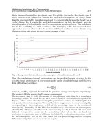
Fig. 6. The PSPWM Dimming Method.
It can be observed from Figure 7 that if the end of the dimming signal for LED array 1 is at
φ
d
, where φ
d
is between φ
k
and φ
k+1
and k ≠ 1, then the output current of the SRC in the range
of φ
k
to φ
k+1
is
⎩
⎨
⎧
≤≤−
≤
≤
=
+1
)1(
kdp
dkp
o
forIk
forkI
i
φφφ
φ
φ
φ
, (17)
New Developments in Liquid Crystals
214
This is also the SRCs output current in each duration from φ
j
to φ
j+1
, where j = 1 to N.
Therefore, the average output current of the SRC is now
[
]
[
]
o
pd
o
d
o
p
o
dp
avgo
IN
N
kNIkkNkI
I
360/
/360
/360)1()1(/360
,
××=
−
×
×
−
+
−
×
−
×
=
φ
φ
φ
, (18)
Fig. 7. Current Waveforms of N Shunt LED Arrays for the PSPWM dimming.
A favored feature is that the load variation of the SRC is always within one step change of I
p
,
no matter what the load level is. Therefore, by carefully designing the duty cycle and the
amplitude of the driving current for each LED array, the no load operation of the DC-DC
SRC may be precluded. Moreover, the output transient of the SRC is improved due to the
confined load change. The number of the LED array for one color, and the peak driving
current of each LED array are first determined according to the specifications of the LED
and the spectrum of the white color. Then a suitable duty cycle is chosen allowing a
reasonable span of variation for dimming control.
4. Single-stage LED backlight circuit
Figure 8 shows a single-stage LED backlight driving system. The backlight driving system
consists of an AHB DC/DC cell integrated with a charge-pump PFC cell. The power
MOSFETs Q1 and Q2, operate with asymmetrical duty ratios, δ and 1-δ, which require short
and well-defined dead time between the conduction intervals. D1, D2 and C
p1
and C
p2
are
the body diodes and the parasitic capacitors of power MOSFETs, respectively. The charge-
pump PFC cell is composed of resonant inductor L
r
, charge-pump capacitors C
r1
and C
r2
,
input diodes D
i1
, and D
i2
, clamping diodes D
c1
, and D
c2
. The capacitor C
bus
is used as the DC
bus capacitor between the charge-pump PFC cell and the post-stage AHB DC/DC cell. The
Introduction to LED Backlight Driving Techniques for Liquid Crystal Display Panels
215
transformer leakage inductor L
l
resonates with the parasitic capacitors C
p1
and C
p2
during
dead-time intervals to achieve zero-voltage switching for the power MOSFETs. The blocking
capacitor C
b
is used to assure that the power sent into the transformer primary winding is a
pure AC type. A DC voltage is supplied to the LED arrays through the secondary rectifier
and filter circuit that are composed of D3, D4, L
o
and C
o
.
Fig. 8. Single-stage LED Backlight Driving System.
The average rectified input current |I
in
|
,av
can be expressed as follows.
inrs
s
av,
in
VCf
T
Q
I
1
==
Δ
, (19)
where ΔQ is the charge variation of C
r1
. From Equation (19), we can see that the average
rectified input current is proportional to the rectified input voltage. Thus, high power factor
can be achieved. Based on the power balance between the input and output of the AC/DC
converter, the following equation has to be satisfied.
in
2
in
o
av,
in
V
V
2P
I
η
=
, (20)
where η and Po are the overall efficiency and output power of the converter. From
Equations (19) and (20), the design equations for the resonant inductor L
r
and the charge-
pump capacitor C
r1
can be derived as follows [22-25].
os
2
in
r
Pf8
V
L
π
η
2
=
, (21)
2
1
2
ins
o
r
Vf
P
C
η
=
, (22)
The ZVS conditions for power switches depend on the resonant inductance current I
Lr
related with the input voltage. At the zero-crossing of input voltage, the resonant
inductance current I
Lr
will be ignorable. Considering the ZVS condition during an entire a
New Developments in Liquid Crystals
216
line period, the transformer leakage inductance L
l
could be determined by using Equation
(23).
2
21
]
I)n ,min(n
Vn
[)CC(L
os2s1
usbp
ppl
+≥
, (23)
In practical design, an external inductor L
e
is usually needed to be added in series connected
with L
l
for satisfying ZVS condition [26-28]. The input current has a near sinusoidal
waveform and in phase with the input voltage. High efficiency and high power factor can be
achieved because of single-stage power conversion with soft-switching features.
5. Conclusion
The advantages of LED backlighting over conventional CCFLs are numerous: fast response,
broader color spectrum, longer life span, and no mercury. However, CCFLs still have cost
advantages. For a LED backlighting, luminous efficacy and thermal management are the
most important issues need to be solved before commercialization. Anyway, rapid advances
in material and manufacturing technologies will enable significant developments in high-
luminance LEDs for backlighting applications. In this chapter, we introduced some LED
backlight driving systems for LCD panels. Dimming control methods are then discussed to
regulate the LED current and brightness for the LED backlight system.
6. References
[1] C. H. Lin, “The Design and Implementation of a New Digital Dimming Controller for the
Backlight Resonant Inverter,” IEEE Trans. Power Electronics, vol. 20, no. 6, pp. 1459-
1466, Nov. 2005.
[2] C. G. Kim, K. C. Lee, and B. H. Cho, “Modeling of CCFL using Lamp Delay and Stability
Analysis of Backlight Inverter for Large Size LCD TV,” IEEE APEC’05, Vol. 3, pp.
1751-1757.
[3] Y. H. Liu, “Design and Implementation of an FPGA-Based CCFL Driving System With
Digital Dimming Capability,” IEEE Transactions on Industrial Electronics, Vol. 54,
Issue 6, pp. 3307-3316, Dec. 2007.
[4] C. H. Lin, “Digital-Dimming Controller with Current Spikes Elimination Technique for
LCD Backlight Electronic Ballast,” IEEE Transactions on Industrial Electronics, Vol.
53, Issue 6, pp. 1881-1888, Dec. 2006.
[5] Y. K. Lo, and K. J. Pai, “Feedback Design of a Piezoelectric Transformer-based Half-
bridge Resonant CCFL Inverter,” IEEE Trans. Industrial Electronics, vol. 54, no. 4, pp.
2716-2723, Oct. 2007.
[6] K. H. Lee, and S. W. R. Lee, “Process Development for Yellow Phosphor Coating on Blue
Light Emitting Diodes (LEDs) for White Light Illumination,” in Proc. Electronics
Packaging Technology Conference, 2006, pp. 379-384.
[7] T. Taguchi, Y. Uchida, and K. Kobashi, “Efficient White LED Lighting and Its
Application to Medical Fields,” Journal of physica status solidi (a), vol. 201, no. 12, pp.
2730-2735, Sept. 2004.
[8] N. Mohan, T. M. Undeland, and W. P. Robbins, “Power Electronics,” USA: John Wiley &
Sons, 2003, pp. 301-313.
Introduction to LED Backlight Driving Techniques for Liquid Crystal Display Panels
217
[9] H. van der Broeck, G. Sauerlander, and M. Wendt, “Power Driver Topologies and
Control Schemes for LEDs,” in IEEE Proc. APEC’07, 2007, pp. 1319-1325.
[10] C. C. Chen, C. Y. Wu, Y. M. Chen, and T. F. Wu, “Sequential Color LED Backlight
Driving System for LCD Panels,” IEEE Transactions on Power Electronics, Vol. 22,
Issue 3, pp. 919-925, May 2007
[11] H. J. Chiu and S. J. Cheng; “LED Backlight Driving System for Large-Scale LCD Panels,”
IEEE Transactions on Industrial Electronics, Vol. 54, Issue 5, pp.:2751-2760, Oct. 2007.
[12] G. Park; T. S. Aum, J. H. Bae, J. H. Kwon, S. K. Lee; M. H. Lee and H. S. Soh,
“Optimization of Direct-type LCD Backlight Unit,” Pacific Rim Conference on Lasers
and Electro-Optics, Aug. 2005, pp. 205-206.
[13] S. Y. Lee, J. W. Kwon, H. S. Kim, M. S. Choi and. S. Byun, “New Design and Application
of High Efficiency LED Driving System for RGB-LED Backlight in LCD Display;”
the 37th IEEE Power Electronics Specialists Conference, June 2006, pp.1-5.
[14] S. Muthu, F. J. Schuurmans, and M. D. Pashley, “Red, Green, and Blue LED based White
Light Generation: Issues and Control,” Annual Meeting. Conference Record of the
Industry Applications Conference, Oct. 2002, Vol. 1, pp. 327-333.
[15] F. Bernitz, O. Schallmoser, and W. Sowa, “Advanced Electronic Driver for Power LEDs
with Integrated Colour Management,” Annual Meeting. Conference Record of the
Industry Applications Conference, Vol. 5, Oct. 2006, pp. 2604-2607.
[16] C. C. Chen, C. Y. Wu, and T. F. Wu, “Fast Transition Current-Type Burst-Mode
Dimming Control for the LED Back-Light Driving System of LCD TV,” IEEE Power
Electronics Specialists Conference, June 2006, pp. 1-7.
[17] Donald A. Neamen, “Electronic Circuit Analysis and Design, 2e,” McGraw-Hill, 2001.
[18] C. C. Chen, C. Y. Wu, and T. F. Wu, “LED Back-light Driving System for LCD Panels,”
IEEE APEC '06, pp. 381-385.
[19] S. Y. Lee, J. W. Kwon, H. S. Kim, M. S. Choi, and K. S. Byun, “New Design and
Application of High Efficiency LED Driving System for RGB-LED Backlight in LCD
Display, ” IEEE PESC '06, pp.1-5.
[20] M. Rico-Secades, A. J. Calleja, J. Ribas, E. L. Corominas, J. M. Alonso, J. Cardesin, and J.
Garcia-Garcia, “Evaluation of a Low-Cost Permanent Emergency Lighting System
based on High-Efficiency LEDs,” IEEE Transactions on Industry Applications, Vol. 41,
No. 5, Sept Oct. 2005, pp.1386-1390.
[21] H. Sugiura, S. Kagawa, H. Kaneko, M. Ozawa, H. Tanizoe, T. Kimura, and H. Ueno,
“Wide Color Gamut Displays using LED Backlight- Signal Processing Circuits,
Color Calibration System and Multi-Primaries,” IEEE ICIP’05, Vol. 2, pp. 9-12.
[22] G. Moschopoulos and P. Jain, “Single-Phase Single-Stage Power-Factor-Corrected
Converter Topologies,” IEEE Transactions on Industrial Electronics, Vol. 52, Issue 1,
pp.23–35, Feb. 2005.
[23] F. S. Kang, S. J. Park, and C. U. Kim, “ZVZCS Single-Stage PFC AC-to-DC Half-Bridge
Converter,” IEEE Transactions on Industrial Electronics, Vol. 49, Issue 1, pp.206-216,
Feb. 2002.
[24] J. Qian, and F. C. Y. Lee, “A High-Efficiency Single-Stage Single-Switch High-Power-
Factor AC/DC Converter with Universal Input,” IEEE Transactions on Power
Electronics, Vol. 13, No. 4, July 1998, pp.699-705.
New Developments in Liquid Crystals
218
[25] J. Qian, and F. C. Lee, “Charge Pump Power-Factor-Correction Technologies. II. Ballast
Applications,” IEEE Transactions on Power Electronics, Vol. 15, No.1, pp. 130-139, Jan.
2000.
[26] F. Bernitz, O. Schallmoser, and W. Sowa, “Advanced Electronic Driver for Power LEDs
with Integrated Colour Management,” IEEE IAS’06, Vol. 5, pp. 2604-2607.
[27] S. Muthu and J. Gaines, “Red, Green and Blue LED-based White Light Source:
Implementation Challenges and Control Design,” IEEE IAS’03, Vol. 1, pp. 515-522.
[28] S. Muthu, F. J. Schuurmans, and M. D. Pashley, “Red, Green, and Blue LED based White
Light Generation: Issues and Control,” IEEE IAS’02, Vol. 1, pp. 327-333.
12
Optoelectronic Device using
a Liquid Crystal Holographic Memory
Minoru Watanabe
Shizuoka University,
Japan
1. Introduction
Recently, the technologies related to liquid crystal spatial light modulators have progressed
dramatically [1]–[4]. Such modulators are classifiable as two types: transmissive and
reflective. Both types are used widely for various applications, e.g. liquid crystal television
panels, personal computer displays, and projector systems. In particular, the resolution of
the latest liquid crystal spatial light modulators in projectors has reached 1,920 pixels × 1,080
pixels, the pixel size of which has also reached 8.5
μ
m × 8.5
μ
m [1], [2] as portrayed in Fig. 1
and Table 1. Therefore, their current resolution and pixel size make them available for use as
holographic media.
Fig. 1. Photograph of a liquid crystal – spatial light modulator (LC-SLM). The modulator is
an LCD panel (L3D07U-81G00 Seiko Epson Corp.)
Open Access Database www.intechweb.org
Source: New Developments in Liquid Crystals, Book edited by: Georgiy V. Tkachenko,
ISBN 978-953-307-015-5, pp. 234, November 2009, I-Tech, Vienna, Austria
New Developments in Liquid Crystals
220
LCD type L3D07U-81G00
Resolution 1,920 x 1,080
Panel size 0.7 inch
Pixel pitch
8.5
μ
m
Aperture ratio 55 %
Table 1. Specifications of the L3D07U-81G00 LC-SLM Panel.
Moreover, recently, optically reconfigurable gate arrays (ORGAs) with a holographic
memory have been developed [5]–[7], [11]–[14], [21]–[23]. The gate array of this
optoelectronic device has a fine grain gate array structure similar to those of field
programmable gate arrays (FPGAs) [8]–[10]. Computations or circuit operations on the gate
array are executed electrically, as they are on FPGAs, whereas configurations and
reconfigurations for the gate array are optically executed. The ORGA architecture has
features of rapid reconfiguration and numerous reconfiguration contexts. Such an optical
reconfiguration architecture often uses liquid crystal spatial light modulators as holographic
memory media [11]–[14], [21]–[23].
Therefore, this chapter first presents the characteristics of a liquid crystal holographic
memory to generate binary patterns. In addition, as an illustration of one application of
liquid crystal devices, this chapter presents discussion of the research of optically
reconfigurable gate arrays (ORGAs).
2. Transmissive-type computer-generated hologram
2.1 Calculation of a holographic memory
This section presents a description of a transmissive-type computer-generated hologram
that can provide two-dimensional binary patterns. Figure 2 presents coordinates of a
hologram plane and an observation plane. Both planes are placed in parallel at a distance of
L. The observation plane is given by the coordinate (x, y); the holographic plane is given by
the coordinate (x
0
,y
0
). An incident light for the holographic memory is assumed as a
collimated monochromatic laser source. The collimated laser beam is incident from the left
side of the holographic memory plane.
Fig. 2. Coordinates for diffraction from a liquid crystal holographic memory.
Optoelectronic Device using a Liquid Crystal Holographic Memory
221
Here, a two-dimensional binary pattern on the observation plane is assumed to be given as a
function O(x,y), which represents a configuration or reconfiguration context in optically
reconfigurable gate arrays (explained later). At that time, the intensity distribution of a
holographic medium is calculable using the following equations.
00
2
(,) (,)sin( ) ,Hx y Oxy rdxdy
π
λ
∞∞
−∞ −∞
∝
∫∫
22 2
00
=()().rLxx yy+−+− (1)
In those equations,
λ
signifies the wavelength, L signifies the distances between the
holographic plane and the observation plane, and r stands for the distance between the
point source
00
(,)Px y
on the holographic memory plane and the point of observation
(,)Qxy . The distance
L
is expected to take (1/4)n
λ
+
, where n is an arbitrary natural
number, to receive the perpendicular incident beam on the observation plane efficiently
with the shortest distance from the holographic memory plane. The value
11
(,)Hxy
is
normalized as 0–1 for the minimum intensity
min
H
and maximum intensity
max
H
, as shown
below.
00
00
(,)
(,)= .
min
max min
Hx y H
Hxy
HH
−
′
−
(2)
Finally, the normalized image
H
′
is used for implementing a holographic memory.
2.2 Diffraction from a holographic memory
Next, the diffraction pattern is estimated from the above calculated holographic memory
pattern. The complex light distribution at the coordinate (x, y) are calculated using the
following equations as
00 00
2
(,) ( , )exp( ) ,
YX
max max
YX
min min
u x y H x y i r dx dy
π
λ
−−
′
∝
∫∫
22 2
00
=()(),rLxx yy+−+− (3)
where
00
(,)Hxy
′
denotes the calculated and normalized holographic memory pattern,
λ
represents the wavelength, L stands for the distances between the holographic plane and the
observation plane, and X
max
, X
min
, Y
max
, and Y
min
respectively represent the holographic
memory sizes. Finally, the diffraction intensity from a holographic memory is calculable as
*
(,)= (,) (,),Ixy uxyu xy (4)
where the superscript asterisk denotes the complex conjugate.
2.3 Single bright bit example in the Fresnel region
In this section, once again, the holographic memory pattern described in section 2.1 is
treated, but in the Fresnel region. If distance L between the two coordinate planes can be
New Developments in Liquid Crystals
222
assumed to be large compared with the sizes of a holographic memory and observation
area, when the following condition is satisfied,
{}
2
223
00
1
()()<<,
4
x
xyy L
λ
−+−
(5)
then r can be approximated to
22
00
()()
,
2
x
xyy
rL
L
−+−
+
(6)
where (x
0
,y
0
) is the coordinate of the holographic memory plane and (x,y) is the coordinate
of the observation plane. Here, assuming that the condition L=
(1/4)n
λ
+
(n = an arbitrary
natural number) is satisfied, then
(1/4)n
λ
+
can be substituted into the first term L of Eq. 6
shown above. Then, substituting Eq. 6 with the condition into Eq. 1, the following equation
is accomplished.
{}
22
00 0 0
(,) (,)cos ( ) ( ) .H x y O x y x x y y dxdy
L
π
λ
∞∞
−∞ −∞
⎛⎞
∝−+−
⎜⎟
⎝⎠
∫∫
(7)
Assuming that the single bright bit is located on the coordinate
(,)
α
β
, the equation O(x,y)
can be considered as
(, )xy
δ
αβ
−
−
. The two-dimensional Dirac delta function
(,)
x
y
δ
is
defined as shown below.
,==0
(,)=
0,
for x y
xy
otherwise
δ
∞
⎧
⎨
⎩
(8)
and
(,) =1.x y dxdy
δ
∞∞
−∞ −∞
∫∫
(9)
When
(,)= ( , )Oxy x y
δ
αβ
−
− , Eq. 7 can be simplified to the following equation.
{}
22
00 0 0
(,) cos ( ) ( ) .Hx y x y
L
π
αβ
λ
⎛⎞
∝−+−
⎜⎟
⎝⎠
(10)
The maximum and minimum of the above equation are, respectively, 1 and -1. Therefore,
the above equation can be substituted into Eq. 2. Finally, the following equation of a
holographic memory pattern including a single bright bit in Fresnel region can be derived.
{}
22
00 0 0
11
(,)=cos ( ) ( ) .
22
Hxy x y
L
π
αβ
λ
⎛⎞
′
−
+− +
⎜⎟
⎝⎠
(11)
This equation represents a Fresnel zone lens, the center of which is located at coordinate
(,)
α
β
. An example of a holographic memory of size of 1.632 mm × 1.632 mm to generate a
single bright bit is shown in Fig. 3. In this example, the holographic memory pattern was
calculated using the condition that the target laser wavelength is 532 nm, the distance L is
100 mm, and the coordinate (
α
,
β
) of a bright bit is (0, 0).
Optoelectronic Device using a Liquid Crystal Holographic Memory
223
Fig. 3. Holographic memory pattern to generate a single bright bit. The size of the
holographic memory pattern is 1.632 mm
× 1.632 mm. The target laser wavelength is 532
nm. The distance L is 100 mm. The coordinate (
α
,
β
) of a bright bit is (0, 0).
It can be confirmed that the holographic memory pattern represents the Fresnel zone lens.
Therefore, a holographic memory pattern to generate a two-dimensional binary pattern with
multi-bright bits becomes a superimposition of the Fresnel zone lens. Next, the diffraction
pattern from the Fresnel zone lens is estimated. The complex light distribution at the
coordinate (x, y) is calculated using the following equation.
{}
22
00
(,) cos ( ) ( ) 1
YX
max max
YX
min min
uxy x y
L
π
αβ
λ
−−
⎧
⎫
⎛⎞
∝
−+− +
⎨
⎬
⎜⎟
⎝⎠
⎩⎭
∫∫
{}
22
00 00
exp ( ) ( ) .ixxyydxdy
L
π
λ
⎛⎞
×−+−
⎜⎟
⎝⎠
Therein,
λ
is the wavelength, L signifies the distances between the holographic plane and the
observation plane, and X
max
, X
min
, Y
max
, and Y
min
respectively represent the holographic
memory sizes. Finally, the diffraction intensity from a holographic memory is calculable as
follows.
*
(,)= (,) (,).Ixy uxyu xy
(12)
Therein, the superscript asterisk denotes the complex conjugate. To produce a compact
system, the system parameters are not always in the Fresnel region. Therefore, at that time,
the Fresnel approximation is inapplicable for calculations and Eqs. 1, 2, 3 and 4 must be
used. However, when the system parameters are in the Fresnel region, the approximation
described above is useful for holographic memory estimations.
3. Optically Reconfigurable Gate Array (ORGA)
Among applications using liquid crystal devices, studies of Optically Reconfigurable Gate
Arrays (ORGAs) exist. Such an ORGA is an optoelectronic device using a liquid crystal
New Developments in Liquid Crystals
224
device as a holographic memory. This device is being developed as an alternative device of
current VLSIs or as a next-generation general-purpose programmable VLSI. The following
section presents a description of the ORGA background and architecture.
3.1 Background
In recent years, SRAM-based Field Programmable Gate Arrays (FPGAs) have been used
widely for large-item small-volume production because of their flexible programmable
capabilities [8]–[10]. Moreover, demand for high-speed reconfigurable devices has been
increasing. If circuit information can be downloaded rapidly from a configuration memory,
idle circuits on a gate array can be removed. At that time, other necessary circuits can be
downloaded from the configuration memory into the gate array, thereby increasing the gate
array's activity. In so doing, high-speed dynamic reconfiguration can increase the
performance of programmable gate arrays. However, since reconfiguration of FPGAs
requires more than several milliseconds, FPGAs are unsuitable for use as dynamically
reconfigurable devices [8]–[10].
However, high-speed reconfigurable devices have been developed: DAP/ DNA chips, DRP
chips, and multi-context FPGAs [15]–[20]. Those devices package reconfiguration memories
and microprocessor arrays or gate arrays onto a chip. The internal reconfiguration memory
stores reconfiguration contexts of 4–16 banks, which can be changed from one to another on
a clock. Consequently, the arithmetic logic unit or gate array of such devices can be
reconfigured on every clock cycle in a few nanoseconds. Nevertheless, an important
problem remains: simultaneously increasing the internal reconfiguration memory while
maintaining the gate density is extremely difficult.
For that reason, optically reconfigurable gate arrays (ORGAs) [5]–[7], [11]–[14], [21]–[23]
have been developed to provide two capabilities: rapid reconfiguration and numerous
reconfiguration contexts. Such optical reconfiguration architecture often uses liquid crystal
spatial light modulators as a holographic memory [11]–[14], [21]–[23]. This chapter presents
a description of the studies of ORGAs with a liquid crystal spatial light modulator.
3.2 Entire construction
An overview of an Optically Reconfigurable Gate Array (ORGA) is shown in Fig. 4. An
ORGA consists of a gate-array VLSI (ORGA-VLSI), a holographic memory, and a laser diode
array. The holographic memory can store numerous reconfiguration contexts. A laser array
mounted on the top of the holographic memory addresses the reconfiguration contexts. The
diffraction pattern from the holographic memory can be received as a reconfiguration
context on a photodiode-array of a programmable gate array on an ORGA-VLSI. Such
ORGA architecture enables microsecond-order reconfiguration and multiple reconfiguration
contexts. Therefore, virtually, the architecture can achieve gate counts larger than the
physical gate count on a VLSI.
3.3 Gate array structure
The basic functionality of an ORGA-VLSI is fundamentally identical to that of currently
available field programmable gate arrays (FPGAs). Figure 5 depicts the gate array structure
of a first prototype ORGA-VLSI. The ORGA-VLSI chip was fabricated using a 0.35
μm
triple-metal CMOS process [12]. A photograph of the board is portrayed in Fig. 6. The
specifications are presented in Table 2. Here, the fundamental function of an ORGA-VLSI is
Optoelectronic Device using a Liquid Crystal Holographic Memory
225
Fig. 4. Overview of an ORGA.
Technology
0.35
μm double-poly
triple-metal CMOS process
Chip size
4.9 mm
× 4.9 mm
Photodiode size
25.5
μm × 25.5 μm
Distance between photodiodes
90
μm
Number of photodiodes 340
Gate count 68
Table 2. ORGA-VLSI Specifications.
described using this chip design as an example of ORGA-VLSI chips. The ORGA-VLSI chip
consists of 4 optically reconfigurable logic blocks (ORLB), 5 optically reconfigurable
switching matrices (ORSM), and 12 optically reconfigurable I/O bits (ORIOB) portrayed in
Fig. 5(a). Each optically reconfigurable logic block is surrounded by wiring channels. One
wiring channel has four connections. Switching matrices are located on the corners of
optically reconfigurable logic blocks and are used as switches of wiring channels. In turn,
the function of each block is described in the following sections.
3.3.1 Optically reconfigurable logic block
A block diagram of an optically reconfigurable logic block is presented in Fig. 5(b). Each
optically reconfigurable logic block consists of a four-input one-output look-up table (LUT),
six multiplexers, four transmission gates, and a delay flip-flop with a reset function. The
input signals from the wiring channel, which are applied from optically reconfigurable I/O
blocks, are transferred to a look-up table through four multiplexers. The look-up table is
used for implementing Boolean functions such as AND circuits, OR circuits, and XOR
circuits. The look-up table construction can be considered as a static memory. For example, a
four-input one-output look-up table can be considered as a static memory with a four-bit
address bus and a single-bit data bus. In this case, the address bus and data bus of the
memory respectively represent signal inputs and signal output of a logic circuit. If some
configuration information, "0001XXXXXXXXXXXX" is programmed to the static memory (X
signifies a do not care state), then the look-up table can function as a two-input one-output
New Developments in Liquid Crystals
226
(a) (b)
(c) (d)
Fig. 5. Gate-array structure of a fabricated ORGA. Panels (a), (b), (c), and (d) respectively
depict block diagram of a gate array, an optically reconfigurable logic block, an optically
reconfigurable switching matrix, and an optically reconfigurable I/O bit.
Fig. 6. Photograph of an ORGA-VLSI board with a fabricated ORGA-VLSI chip. The ORGA-
VLSI was fabricated using a 0.35
μm three-metal 4.9 × 4.9 mm
2
CMOS process chip. The gate
count of a gate array on the chip is 68. In all, 340 photodiodes are used for optical
configurations.
Optoelectronic Device using a Liquid Crystal Holographic Memory
227
AND circuit. In this case, two multiplexers connected to upper two bits of the look-up table
must be programmed to be L. The multiplexers connected to the inputs of look-up table can
choose L, H, and two signals of the wiring channel for the look-up table inputs. In addition,
the output of the look-up table is connected to a multiplexer through a delay type flip-flop.
Therefore, a combinational circuit and sequential circuit can be chosen by changing the
multiplexer. Finally, an output through the multiplexer from the look-up table is connected
to the wiring channel through transmission gates, again. The last multiplexer controls the
reset function of a delay-type flip-flop. Such a four-input one-output look-up table, each
multiplexer, and each transmission gate respectively have 16 photodiodes, two photodiodes,
and one photodiode. In all, 32 photodiodes are used for programming an optically
reconfigurable logic block. In Fig. 5(b), the P mark shows a photodiode. In this optically
reconfigurable logic block, although eight other photodiodes were implemented for special
use of a differential reconfiguration strategy, that method is described in earlier reports [12],
[21].
3.3.2 Optically reconfigurable switching matrix
Similarly, optically reconfigurable switching matrices are optically reconfigurable. A block
diagram of the optically reconfigurable switching matrix is portrayed in Fig. 5(c). The basic
construction is the same as that used by Xilinx Inc. One four-directional with 24
transmission gates and 4 three-directional switching matrices with 12 transmission gates
were implemented in the gate array. In this construction, a connection in any direction can
be realized using a transmission gate so that propagation delay can be decreased compared
with the case using four transmission gate passes. Each transmission gate can be considered
as a bi-directional switch. A photodiode is connected to a transmission gate and controls
whether the transmission gate is closed or not. Based on that capability, four-direction and
three-direction switching matrices can be programmed, respectively, as 24 and 12 optical
connections.
3.3.3 Optically reconfigurable I/O block
Optically reconfigurable gate arrays are assumed to be reconfigured frequently. For that
reason, an optical reconfiguration capability must be implemented for optically
reconfigurable logic blocks and optically reconfigurable switching matrices. However, the
I/O block might not always be reconfigured under such dynamic reconfiguration
applications because such a dynamic reconfiguration arises inside the device and each state
of Input, Output, or Input/Output, and each pin location of the I/O block must always be
fixed because of limitations of an external environment. However, the ORGA-VLSI support
optical reconfiguration for I/O blocks because optical reconfiguration information is
provided optically from a holographic memory in ORGA. Consequently, electrically
configurable I/O blocks are unsuitable for ORGAs. Here, each I/O block is also controlled
using nine optical connections. Always, the configuration of the optically reconfigurable I/O
block is executed only initially.
3.3.4 Physical implementation
Because the ORGA-VLSI has 340 photodiodes to program its gate array, the ORGA-VLSI
can be reconfigured rapidly and perfectly in parallel. In this fabrication, the distance
New Developments in Liquid Crystals
228
between each photodiode was designed as 90
μm. The photodiode size is set as 25.5 × 25.5
μm
2
to ease optical alignment. The photodiode was constructed between the N-well layer
and P-substrate. The gate array's gate count is 68. It was confirmed experimentally that the
ORGA-VLSI itself is reconfigurable within 10 ns.
4. Nine-configuration-context ORGA
This section presents an implementation example of a nine-configuration context ORGA.
4.1 Experimental system
An ORGA holographic memory system with nine configuration contexts using a liquid-
crystal spatial light modulator (LC-SLM) as a holographic memory, nine 532 nm, 300 mW
lasers (in the actual implementation, one laser emulated the nine lasers), and an ORGA-VLSI
are depicted in Fig. 7. Each laser corresponds to a configuration context or a holographic
recording area including the single configuration context and is used for addressing the
configuration context. First, a nine-context holographic memory pattern is calculated using
Eqs. 1 and 2. Here, distance L between a holographic memory and an ORGA-VLSI is 100
mm. The wavelength
λ
is 532 nm. The target LC-SLM is a projection TV panel (L3D07U-
81G00; Seiko Epson Corp.). It is a 90° twisted nematic device with a thin-film transistor. The
panel has 1,920
× 1,080 pixels, each of 8.5 × 8.5 μm
2
, with 256 gradation levels. The calculated
holographic pattern shown in Fig. 8(a) is displayed on the LC-SLM. The number of pixels of
each recording area, including one reconfiguration context, is 450
× 250. Each interval
between recording areas is 5 pixels. Therefore, the entire holographic memory pattern is
1,360 pixels
× 760 pixels. Each laser beam is collimated: the beam is incident to its
corresponding holographic recording area on the LC-SLM. By turning on a certain laser, one
configuration context can be programmed onto the ORGA-VLSI. Optically parallel
programming enables very high-speed configuration and reconfiguration.
Fig. 7. ORGA system using a liquid crystal spatial light modulator as a holographic memory.
Optoelectronic Device using a Liquid Crystal Holographic Memory
229
(a)
(b) (c)
Fig. 8. (a) Holographic memory pattern, and CCD-captured images of configuration contexts
of (b) an AND and (c) a NOR circuits.
4.2 Configuration experiments
Here, among the nine configuration contexts, two configuration experiments of an AND
circuit and a NOR circuit are introduced. A configuration context of an AND circuit was
programmed at the top-left side of the holographic memory, while a configuration context
of a NOR circuit was programmed at the bottom-left side of the holographic memory.
Figures 8(b) and 8(c) depict CCD-captured images of configuration contexts of the AND
circuit and the NOR circuit at the position of the ORGA-VLSI. Figure 9 shows that the AND
circuit was programmed correctly onto ORGA-VLSI and that the AND circuit functioned
correctly. Here, the configuration period of the AND circuit is 5
μs. Figure 10 shows that the
NOR circuit was programmed correctly onto ORGA-VLSI and that the circuit functioned
New Developments in Liquid Crystals
230
correctly. The configuration period of the NOR circuit was measured as 4
μs, thereby
confirming the rapid configuration capability of the nine-configuration-context ORGA
architecture.
Fig. 9. 5
μ
s configuration result of an AND circuit.
Fig. 10. 4
μ
s configuration result of an NOR circuit.
4.3 Response time of the liquid-crystal holographic memory
Next, the response time of a liquid-crystal holographic memory is estimated. The turn-on
and turn-off times were measured experimentally using an L3D07U-81G00 panel provided
by Seiko Epson Corp. The results show that the turn-on time is less than 12 ms. The turn-off
time is less than 2 ms, as shown in Fig. 11.
5. Acceleration method
A liquid-crystal holographic memory is an easily rewritable material. For that reason, many
reconfiguration contexts can be supplied dynamically to a gate array. Of course, a liquid-
Optoelectronic Device using a Liquid Crystal Holographic Memory
231
Fig. 11. Response time measurement of a liquid crystal holographic memory. The turn-on
and turn-off times were measured experimentally using an LCD panel (L3D07U-81G00;
Seiko Epson Corp.) Results show that the turn-on time is less than 12 ms; the turn-off time is
less than 2 ms.
crystal holographic memory requires a period of a few milliseconds for changing
holographic contexts. However, once a liquid-crystal holographic memory stores a
holographic configuration context array, the holographic memory can successively write
New Developments in Liquid Crystals
232
configuration contexts of the holographic configuration context array onto the gate array.
Consequently, although a context preparation for a liquid-crystal holographic memory takes
a long time, once it is completed, rapid configurations can be done easily. The average
configuration time becomes the value of the response time of the liquid-crystal holographic
memory divided by the array number of holographic configuration context array if it is
assumed that the laser reconfiguration period is negligible compared to the response time of
a liquid-crystal holographic memory. Therefore, when each configuration time T
Conf.
is much
smaller than the switching time T
LC
of a liquid-crystal holographic memory, the equation is
estimated as the following.
.
L
C
Virtualcycle
T
T
N
(13)
As configuration contexts become more numerous in the future, this architecture is expected
to become increasingly useful.
6. Conclusion
This chapter has described an optically reconfigurable gate array (ORGA) with an LC-SLM
and a reconfiguration-speed acceleration method. The ORGA architecture has enabled the
achievement of microsecond-order reconfiguration and nine configuration contexts.
Although the LC-SLM response time is not faster than that of silicon devices, the use of
multiple configurations decreases the average configuration period. Based on that
improvement, this easily programmable LC-SLM was demonstrated as useful for ORGA
applications.
Fig. 12. Successive configuration method for a liquid crystal holographic memory. The
figure presents an example of a four-context liquid crystal holographic memory. In this case,
successive configurations can be executed as three or four times faster than the switching
speed of the liquid crystal holographic memory.