Development and Implementation of RFID Technology Part 2 potx
Bạn đang xem bản rút gọn của tài liệu. Xem và tải ngay bản đầy đủ của tài liệu tại đây (2.88 MB, 30 trang )
Design of Antennas for RFID Application
21
be the antenna impedance normalized to the real part of the chip impedance, then
2
2
1
1
a
a
Z
s
Z
−
=
+
, or
1
1
a
a
Z
s
Z
−
=
+
. (21)
On the basis of the transformation, the traditional Smith Chart can be used to describe the
impedance match between the antenna and the chip.
a
Z
can be marked according to its real
part and imaginary part on Smith Chart like the traditional normalized impedance. The
distance between the point of each
a
Z
and the centre point of Smith Chart expresses the
magnitude of the complex power reflection coefficient s, while the trace of impedance
points, which have a constant distance to the centre point, forms the concentric circle, which
is called as the equivalent power reflection circle. The centre point of Smith Chart is the
perfect impedance match point, while the most outer circle denotes the complete mismatch
case, i.e.
1s = .
The power transmission coefficient (Rao, Nikitin & Lam, 2005b) can also be defined as
τ
,
and
ca
PP
τ
= , where
a
P stands for the power from reader caught by tag antenna,
c
P the
power transmitted from the tag antenna to the tag chip. It follows from Fig. 3 that
2
4
,0 1
ca
ac
RR
ZZ
ττ
=
≤≤
+
(22)
2
1s
τ
+
= (23)
Let
a
a
c
X
x
R
= ,
a
a
c
R
r
R
= ,
c
c
c
X
Q
R
= , then equation of the circle with constant power
transmission coefficient is expressed as follows.
22
2
24
[(1)][ ] (1)
aac
rxQ
τ
ττ
−
−++ = − (24)
From equation (24), the impedance chart with the constant power transmission coefficient is
draw, as shown in Fig. 4.
In Fig. 4, the x axis expresses the normalized real part
/
aac
rRR
=
, and y axis the
normalized imaginary part
/
aac
x
XR
=
. The circles with constant power transmission
coefficients
τ
=1, 0.75, 0.5, 0.25 are draw in Fig. 4. The x axis is called as the resonant line
with
ac
X
X=− , while the y axis is called as the complete mismatch line. When
τ
’s
decrease, the radius of the circles with constant power transmission coefficient increase.
While
0
τ
→
, the circle with constant power transmission coefficient approaches to its
tangent, that is the y axis, on which the impedance point cannot achieve the power
transmission.
When the chip and the antenna are resonant,
ac
X
X
=
− , and
ac
x
Q
=
− , then equation
(24) becomes
Development and Implementation of RFID Technology
22
Fig. 4. The impedance chart with the constant power transmission coefficient
2
2
24
[(1)] (1)
a
r
τ
τ
τ
−
−= −
(25)
2
[(2)]4(1)
a
r
τ
ττ
−
−=−
(26)
Making the derivative for the both sides of equation (26), we have
2[ (2 )]( ) 4
aa
aa a
dd d
rr
dr dr dr
τ
ττ
τττ
−− + + =−
(27)
[( 1) 2]
2
a
aa
r
d
dr r
τ
τ
τ
+
−
=
(28)
Obviously 1
τ
= means perfect match, and
0
a
d
dr
τ
=
. 0
τ
=
means complete mismatch,
and
0
a
d
dr
τ
=
. Thus either the perfect match or the complete mismatch is a steady point of
τ
with
a
r , i.e.
0
a
d
dr
τ
=
.
Design of Antennas for RFID Application
23
For the fixed
a
c
R
R
and
a
c
X
X
,
22 2
44
| 1 (1 ) | (1 ) (1 )
aa
cc
aaa a
cc
ccc c
RR
RR
RXR X
jQ Q
RXR X
τ
==
++ + + + +
(29)
22222
8(1 ) [(1 ) (1 )]
aa a a
cc
ccccc
XR R X
d
dQ X R R X
τ
−
=− + + + +
(30)
When the chip impedance is capacitive, i.e.
0
c
Q
<
, it follows from (13) that
0
c
d
dQ
τ
>
.
While the chip impedance is inductive, i.e. 0
c
Q > ,
0
c
d
dQ
τ
<
. When 0
c
Q
=
, i.e. 0
c
X =
and meanwhile
0
a
X
=
, we have
2
4
()
ca
ca
RR
RR
τ
=
+
(31)
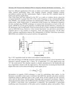
The curve of
τ
versus Qc is shown in Fig.5. From this figure, we can see that for the fixed
a
c
R
R
and
a
c
X
X
, Qc should be as small as possible from the power transmission point of view,
when the tag antenna is connected to the tag chip.
For the tag antenna, the impedance chart can be used to guide the design or to describe the
tag antenna. The chart is theoretically important and very useful for other applications.
Fig. 5. Curve of
τ
versus Qc
3.2 Impedance design for the tag antenna
Aforementioned results indicate that the maximum power transmission can be realized only
if the antenna impedance is equal to the conjugate value of the chip impedance. While the
Development and Implementation of RFID Technology
24
chip impedance is not normal 50 ohm or 75ohm, the structure of the tag antenna should be
carefully chosen. In this section, a symmetrical inverted-F metallic strip with simple
structure shown in Fig. 6 is proposed.
The antenna has the ability to realize several impedances. For UHF band application, the
impedance of the antenna in four cases with different structure parameters is analyzed at
912MHz, whose real part is approximately 22ohm, 50ohm, 75ohm, 100ohm respectively. The
simulated results for these four cases are shown in Fig. 7.
Fig. 6. The symmetrical inverted-F Antenna
72 76 80 84 88 92
-300
-200
-100
0
100
Z
a
=R
a
+jX
x
L1
R
a
X
a
80 85 90 95 100
-200
-100
0
100
200
Z
a
=R
a
+jX
a
L1
R
a
X
a
(A) W=30mm, L2=10mm (B) W=50mm, L2=25mm
80 85 90 95 100
-100
0
100
200
Z
a
=R
a
+jX
a
L1
R
a
X
a
70 75 80 85 90
-200
-100
0
100
Z
a
=R
a
+jX
a
L1
R
a
X
a
(C) W=64mm, L2=32mm (D) W=73mm, L2=32mm
Fig. 7. Impedance results of the antenna in different cases
Design of Antennas for RFID Application
25
Fig. 7 shows that the symmetrical inverted-F metallic strip can realize several impedance
values by adjusting its short branch. A lot of familiar types of tag antennas are the
modifications or transformations of this structure (Dobkin & Weigand, 2005).
Fig. 8 shows the evolvement of several tag antennas. Antenna B has less influence on its
performance than antenna A, when the antenna is curved (Tikhov & Won, 2004). Antennas
C and D are fed by an inductively coupled loop (Son & Pyo, 2005).
Fig. 8. Evolvement of the tag antennas
Fig. 9. Geometry of a meandered dipole antenna surrounded by the rectangular loop
(dimensions in mm)
In our application, an UHF band tag chip with 43-j800 ohm impedance is used, and a tag
antenna connected to this chip should match the tag chip. Meanwhile the tag antenna
should be small in size and easily fabricated. In Fig. 9, a meandered dipole antenna is
designed, and a pair of symmetrical meandered metallic strips surrounded by a rectangular
AB
CD
Development and Implementation of RFID Technology
26
loop is fed. The higher real part of the impedance can be realized by the meandered dipole,
while its high imaginary part can be supplied by the coupling between rectangular loop and
symmetrical meandered dipole. In this way, a tag antenna with higher absolute value
impedance and higher Q value is designed and connected to the chip, to ensure the good
power transmission. The gap of the feeding point is 0.1mm, the width of the metallic
meandered strip and the horizontal part of the rectangular loop is 1mm, and the width of its
vertical part is 2mm. The tag antenna has a thickness of 0.018mm.
The tag antenna is analyzed by the HFSS software, the performance of the antenna,
including its impedance and radiation patterns, is calculated. The simulated results are
shown in Table 1 and Fig. 10. These results show that the antenna with small size can be
used as a tag antenna for the UHF band RFID chip application.
Freq(MHz)
Antenna
impedance
(ohm)
Power reflection
coefficient
2
s
Power transmission
coefficient
τ
900 36.6+j695.2 0.6365 0.3635
901 37.1+j701.6 0.6036 0.3964
902 37.7+j708.0 0.5670 0.4330
903 38.3+j714.5 0.5268 0.4732
904 38.9+j721.0 0.4833 0.5167
905 39.5+j727.7 0.4354 0.5646
906 40.1+j734.5 0.3840 0.6160
907 40.7+j741.4 0.3294 0.6706
908 41.3+j748.4 0.2728 0.7272
909 42.0+j755.5 0.2152 0.7848
910 42.7+j762.7 0.1593 0.8407
911 43.4+j770.0 0.1076 0.8924
912 44.1+j777.4 0.0632 0.9368
913 44.8+j785.0 0.0288 0.9712
914 45.5+j792.7 0.0076 0.9924
915 46.3+j800.5 0.0014 0.9986
916 47.1+j808.4 0.0107 0.9893
917 47.9+j816.4 0.0343 0.9657
918 48.7+j824.6 0.0707 0.9293
919 49.6+j832.9 0.1166 0.8834
920 50.4+j841.4 0.1695 0.8305
921 51.3+j850.0 0.2255 0.7745
922 52.2+j858.7 0.2822 0.7178
923 53.2+j867.6 0.3381 0.6619
924 54.1+j876.7 0.3923 0.6077
925 55.1+j885.9 0.4426 0.5574
926 56.1+j895.2 0.4890 0.5110
927 57.2+j904.8 0.5320 0.4680
928 58.3+j914.5 0.5710 0.4290
929 59.4+j924.4 0.6065 0.3935
930 60.5+j934.5 0.6387 0.3613
Table 1. The impedance and power reflection coefficient, power transmission coefficient for
Tag antenna(chip impedance: 43-j800ohm)
Design of Antennas for RFID Application
27
-40
-30
-20
-10
0
0
30
60
90
120
150
180
210
240
270
300
330
-40
-30
-20
-10
0
E pl ane
H pl ane
Fig. 10. Radiation pattern of the meandered dipole antenna
3.3 Tag antenna mountable on metallic objects
Since the RFID technology is applied in wide fields, RFID systems frequently appear in the
metallic environment, and the effect of the metallic objects should be considered in
designing the antenna (Penttilä et al, 2006). RFID antennas in microwave band have a defect
of standing wave nulls under the impact of metallic environment. To solve the problem
brought by the metallic objects, some special tag antennas should be designed. These
antennas usually have a metallic ground. Some metallic objects, which make the
performance of the RFID antenna worse, are modified to be as an extended part of the
antenna to improve its performance. Some existing problems should be discussed.
When the traditional dipole antenna is attached to an extremely large metallic plane, its
radiation will be damaged. In general, the tag antenna with a hemispherical coverage is
required. In practical application, a tag antenna with low profile is frequently used, and its
vertical current is limited. In Fig. 11, when a normal dipole antenna approaches closely the
metallic surface, an inductive current in opposite direction is excited, and the radiation
induced by the current will eliminate the radiation of the dipole, resulting in that the tag
cannot be detected or read. As a class of antennas, the microstrip antenna may be a good
choice for being mounted on the metallic surfaces and identifying the metallic objects. For
ordinary tag chip, a balun or other circuit is needed to feed the antenna. Here, based on the
dipole antenna, two design schemes for the metallic surfaces are proposed. One is a
modification to the Yagi antenna, and the other is a dipole Antenna backed by an EBG
structure. A substrate with high dielectric coefficient is sandwiched between the dipole and
the metallic surface, its thickness will reverse the orientation of the inductive current, and
the radiation is strengthened. An EBG structure can depress the primary inductive current,
Development and Implementation of RFID Technology
28
the radiation of the dipole will be available, and the metallic surface of the identified object
is also the ground of the EBG structure.
Fig. 11. Design scheme for the tag antenna on metallic surfaces
(a) Excitation current nearby the metallic surface; (b) Scheme based on the Yagi antenna
(c) Scheme based on the EBG structure
According to the introduced schemes, three tag antennas are designed for three tag chips
with impedances 15-j20 ohm (chip 1), 6.7-j197ohm (chip 2), and 43-j800 ohm (chip 3),
respectively. The tag antenna based on the Yagi antenna is shown in Fig. 12, and the
geometry of the active dipole (Qing & Yang, 2004a) is also given in Fig. 13. In Fig.12, the
active dipole is attached on the substrate with the relative dielectric coefficient εr=10.2. The
width of the metallic strip is 0.8mm.
Fig. 12. The tag antenna for chip 1 based on the Yagi antenna
Design of Antennas for RFID Application
29
Fig. 13. Geometry of the active dipole (dimensions in mm)
The antenna shown in Fig. 12 is analyzed by the HFSS software. The calculated antenna
impedance matches the chip impedance 15-j20 ohm in UHF band. Radiation patterns of the
tag antenna are also calculated and shown in Fig. 14.
To design the antenna for chip 2 with 6.7-j197 ohm impedance, the structure parameters are
adjusted. The designed dipole is shown in Fig. 15, and its simulated radiation patterns are
presented in Fig. 16.
-20
-10
0
10
0
30
60
90
120
150
180
210
240
270
300
330
-20
-10
0
10
E pl ane
H pl ane
Fig. 14. Radiation patterns of the tag antenna for chip 1
Development and Implementation of RFID Technology
30
(1) The tag antenna and the substrate (2) The active dipole
Fig. 15. Geometry of the tag antenna for chip 2
-20
-10
0
10
0
30
60
90
120
150
180
210
240
270
300
330
-20
-10
0
10
E plane
H plane
Fig. 16. Radiation patterns of the tag antenna for chip 2
Similar tag antenna can also be designed based on the EBG structure (Abedin & Ali, 2005a,
2005b, 2006; Yang & Rahmat-Samii, 2003) like the tag antenna shown in Fig. 12. The EBG
structure is attached to the surface of the metallic object, and the tag dipole antenna like the
active dipole in Fig. 13 is placed on the EBG structure formed by 5×7 elements, as shown in
Fig. 17. This structure is analyzed at frequency 915MHz in the UHF band, and its radiation
patterns are calculated, which are shown in Fig. 18. The simulated impedance values show
that the tag antenna matches the chip 3 with impedance 43-j800 ohm. The relative dielectric
coefficient of the substrate of the EBG structure is 2.65, its thickness is 2mm, and the total
thickness of the tag antenna is 15mm. The low cost tag antenna with low profile will be
fabricated.
Design of Antennas for RFID Application
31
Fig. 17. The tag antenna backed by the EBG structure for chip 3
-30
-20
-10
0
10
0
30
60
90
120
150
180
210
240
270
300
330
-30
-20
-10
0
10
E plane
H plane
Fig. 18. Radiation patterns of the dipole backed by the EBG structure for chip 3
In this section, design of the tag antenna for the metallic surface is presented, and several
cases are described and discussed. Other types of tag antenna mounted on the metallic
objects, such as the inverted-F antenna and its modifications are also popular. For the details
about these antennas, refer to Kim et al., 2005; Son et al., 2006; Ukkonen, Sydänheimo et al.,
2004; Hirvonen et al., 2004; and Ukkonen, Engels et al., 2004.
4. Circular polarization modulation and design of the circularly polarized
antennas
4.1 Circularly polarized reader antenna and circular polarization modulation
Generally the object to be identified or the tag does not point to a certain direction, so the
circularly polarized reader antennas are usually used (Raumonen et al., 2004) to receive
signals from all directions and do not miss the mismatched polarized signals of the moving
object. The linearly polarized reader receives more than 3dB power, when the polarizations
of the tag and the reader are matched. In some wireless communication systems, the circular
Development and Implementation of RFID Technology
32
polarization modulation (Fries et al., 2000; Kossel, Kung, et al., 1999), which is well adapted
to the low rate RFID systems, is another choice that can reduce the requirement of the
frequency band, and simplifies the data communication, as shown in Fig. 19. Therefore, the
antennas, used for the reader and the tag, should be dual circular polarization antennas with
two ports in the RFID system.
Fig. 19. Principle chart of the circular polarization modulation
Helix antennas and microstrip antennas are widely used as the circularly polarized reader
antenna for one-port applications. The helix antenna has some advantages, such as low cost
and simple design, except its larger physical size. The low profile helix antenna with the
EBG structure instead of the metal ground plane can be used for the RFID reader
(Raumonen et al., 2004).
The circular polarization modulation is always used in the RFID system, and its basic
principle is that a logical zero is transmitted as the left-hand circularly polarized (LHCP)
wave, and a logical one is represented by a right-hand circularly polarized (RHCP) wave.
Both reader and tag can use circularly polarized antennas with switchable polarizations.
Cross polarization isolation has the significant effect on the performance of the whole
Design of Antennas for RFID Application
33
system. The maximum transmission distance can be expanded more than 20%, if the cross
polarization level (XPL) reaches up to 20dB from 5dB. In the backscattering modulation
system, the incident LHCP wave illuminated to the tag is modulated and backscattered into
the RHCP wave, and then retransmitted to the reader. Relative to the system where the
linearly polarized tag antennas are used, the signal received by the reader in the circular
polarization modulation system will raise 6dB. In spite of what kind of the modulation is
used, the system should have higher polarization isolation. At the same time, the tag
antenna should have higher port isolation, which can reduce the interference between the
transmission channel and the receive channel.
Fig. 20. The 3dB branch line directional coupler structure
Fig. 21. Microstrip antenna with coupling slot based on the branch line coupler
The traditional design of the dual-port dual-polarization antenna (Kossel, Benedickte et al,
1999; Qing & Yang, 2004b; Sharma et al., 2004) is based on the branch line directional
coupler, in which the electrical fields in two output branches have identical voltages and a
90º phase shift, and has high isolation between two output ports, as shown in Fig. 20. When
the impedances of the four ports are matched very well and the signal inputs from Port 1,
Port 4, called the isolation port, has no output signal, and there is a 90º phase shift between
Port 2 and Port 3. The dual circularly polarized antenna, as shown in Fig. 21, is a microstrip
Development and Implementation of RFID Technology
34
patch antenna, which uses a branch line coupler to feed the orthogonal slot apertures and to
realize the required 90º phase shift. Four different circularly polarized antennas are shown
in Fig. 22. The multilayered antennas employ two substrates, the patch layer and the feed
layer, and a ground plane with slot apertures between two substrates, as shown in Fig. 23.
The patch antennas can realize the dual circular polarization by using the branch line
coupler or the microwave branches to feed the slot apertures with the required phase shift.
Fig. 22. Four dual-port dual circularly polarized antennas
Fig. 23. Multilayered microstrip antenna structure
Design of Antennas for RFID Application
35
4.2 A compact dual circularly polarized antenna
In order to realize low profile and part the feed line from the patch, the slot aperture
microstrip antenna is commonly used. For this kind of antennas, the designer could select
different substrates for the feed and patch layers, according to the application requirements
of the microwave integrate circuits. As shown in last section, dual circularly polarized
antennas for the RFID system in microwave band are fed by two orthogonal and isolated
slot apertures, based on the branch line directional coupler or other complex microwave
networks. However, the configuration of the antenna presents a structural bottleneck, i.e.
the isolated slots and feeding network limit the miniaturization of the antennas, and the
microwave network with complex circuits occupies the larger space. It is well known that
RFID antennas can achieve long distance propagation of electromagnetic waves, but
sometimes have the problem such as standing wave nulls. Therefore, the antennas should be
integrated with the loop, which could transmit power to the low frequency system through
the inductance coupling, and reduce the size of the feed network. In order to get rid of the
bottleneck on the miniaturization of the antennas, we should design the compact slot
aperture microstrip antenna with simple feed network to accomplish the dual circular
polarization. In this section, we present a compact dual circularly polarized antenna for
RFID systems.
In the RFID system, the rate of the data communication is not so high, sometimes just a few
bites. Therefore the circular polarization modulation can be used in the narrow bandwidth
communication to simplify the data communication. It is necessary to design dual circularly
polarized antenna with two well-isolated ports for the circular polarization modulation.
In order to miniaturize the dimensions of the antenna, as shown in Fig. 24, a dual circularly
polarized microstrip antenna fed by crossed slots without the branch line coupler is
proposed (Zhang, Chen., Jiao & Zhang, 2006), which is an optimal choice for the RFID
system with larger bandwidth and the smaller size. The coupling aperture for the circularly
polarized antenna comprises two crossed slots (Aloni E. & Kastener, 1994) in the ground
plane, with four arms of the aperture fed serially by a single microstrip line located
underneath the ground plane. The microstrip line feeds the four arms with 90º progressive
(a) Top view (b) Side view
Fig. 24. Structure of the dual circular polarized antenna
Development and Implementation of RFID Technology
36
phase difference. The symmetric arrangement makes the antenna achieve easily the dual
circular polarization. The design method has been widely used for the antenna at 2.45GHz
in the RFID system.
In order to reduce the cost, the air layer used to replace the foam material, as shown in Fig.
24, is sandwiched between two substrate layers with the same dielectric constant εr=2.65.
HFSS simulation results show that the performance of the antenna cannot satisfy the
requirement for the RFID system. Thus, the structure of the antenna should be modified to
improve its performance. As a result, a corner-truncated square patch (Wang, 1989) is used
to replace the normal square patch, which will improve the circular polarization
performance of the antenna and its port characteristics. At the same time, we cut a square
aperture in the centre of the patch to restrict the current and to improve the port isolation.
Steps of the patch evolution from the square to the corner-truncated square with a square
aperture are shown in Fig. 25, and the final antenna structure is shown in Fig. 26. Simulated
performance indices of these three patch antennas are given in Table 2, which indicate the
effectiveness of the patch modifications.
Fig. 25. Steps for the patch modifications
Fig. 26. Geometry of the antenna after modifications
Design of Antennas for RFID Application
37
We now determine the dimensions of the corner-truncated square patch antenna with a
square slot. First we adjust the dimension of the patch to get the maximum gain, keeping the
other parameters of the antenna fixed. We then adjust the length and width of the slots to
improve the port characteristics. Because it affects the coupling between the microstrip and
the patch more seriously, the length of the slots should be adjusted in advance. Finally, by
adjusting the square aperture and the corner of the patch, the antenna with better
performance is obtained. The total size of the antenna is 60mm×60mm× 3mm. The width of
the corner-truncated square patch with a square aperture is 51mm, and each layer is 1mm
thick. The microstrip line has a width that makes the transmission line have 50Ω
characteristic impedance. The length and width of the aperture are 24mm and 0.316mm,
respectively.
Patch modifications
Axial Ratio (dB) S11 (dB) S21 (dB)
Primary square patch 3.64 -11 -17
Corner-truncated square patch 0.73 -20.2 -19.2
Final patch structure 1.07 -20.4 -30
Table 2. Antenna parameters during the modification
We have tested a prototype of the compact dual circularly polarized antenna shown in Fig.
29. The measured results are shown in Figs. 27 and 28. Comparison between the simulated
results and the measured data shows that the measured S parameters at two ports agree
well with the simulated results. The measured S21 is better than the simulated one, however
the measured S11 is worse than the simulated one. There is a tradeoff between the return
loss and the port isolation. From the measured radiation patterns, we can see that the cross
polarization levels better than -15 dB are achieved. Although the measured cross
polarization levels cannot reach the simulated circular polarization performance, they meet
the requirements of the RFID system. The antenna can be used to realize the circular
polarization modulation for the RFID systems.
2.35 2.40 2.45 2.50
-50
-40
-30
-20
-10
0
dB
S11
S22
S21
Fig. 27. Measured S parameters at two ports
Development and Implementation of RFID Technology
38
Simulated and measured results for the compact dual circularly polarized aperture coupled
patch antenna show that the compact structure meets the requirements for the RFID system.
For the antenna with smaller size, a port decoupling better than 20 dB and a good circular
polarization are achieved by the coupling and feeding technique, without using the
microstrip branch line coupler or other complex feed networks. The design can save more
space for the IC layout, and the miniaturization of the antenna is realized, which is very
important for the integration of the RFID system at the microwave frequency and low
frequency bands. The dual circularly polarized antenna with the compact structure is not
only applicable to the normal RFID systems, especially in some identification card
applications, but also suitable for using in some wireless communication systems.
-2 00 -100 0 100 20 0
-30
-20
-10
0
Re l.Power (dB)
Co- Polarization
Cross-Polarization
-200 -100 0 100 200
-30
-20
-10
0
Rel.Power (dB)
Co-Polarization
Cross-Polarization
(a) (b)
Fig. 28. Measured radiation patterns at two ports
(a) Excitation in LHCP port; (b) Excitation in RHCP port
Fig. 29. Photograph of the compact dual circularly polarized antenna prototype
5. Design of antennas for the RFID tag in microwave bands
According to the design of the tag and the reader at the microwave band, special chips for
the application of the RFID system are immature and seldom used in industry. Thus
engineers usually use specific ASICs available in the market for some special RFID systems,
Design of Antennas for RFID Application
39
and sometimes use the coaxial cable to connect the ASIC with the antenna, whose
impedance is 50Ω.
A radio-frequency identification system consists of tags and readers, and readers
communicate wirelessly with the tags to obtain or transfer the information. The data sent by
the reader is modulated and backscattered from a number of tags. In some cases, the reader
changes the data stored in the tag. Several frequency bands, such as 125 KHz, 13.56 MHz,
869 MHz, 902-928 MHz, 2.45GHz and 5.8GHz bands, have been assigned to the RFID
applications. As the operating frequency for the RFID systems rises into the microwave
bands, the antenna design becomes more acute and essential (Chen & Hsu, 2004; Liu & Hu,
2005).
The tag, which includes the antenna and a microchip transmitter, must be low in profile,
low in cost and small in size for the valuable and easy use, when it is attached to an object to
be identified. Therefore, a suitable antenna used in the tag becomes more and more
important. As the RFID technology continues to be widely used in applications, especially
meeting the reliability, the anti-interfere and the other special requirements, the systems that
are able to work at two bands, such as 2.45GHz and 5.8GHz bands, are expected.
The reader with a single antenna is used for both data transmission and receiving, which
needs severe operational requirements to the reader RF front end, since the communication
takes place in both directions at the same time. The reader may use two antennas for the
communication, one antenna for the data transmission and the other antenna for the data
receiving (Penttilä et al, 2006). This choice can reduce the realization difficulty from the
hardware point of view. In addition, there may have more than two antennas in the reader.
In this case, the reader must follow a certain sequence to switch on an antenna at a time,
while keeping other antennas switched off, to avoid interferences between these antenna
signals.
The approach for using two antennas in the reader is based upon the following reasons:
1. The transmitting electromagnetic wave from the reader does not vanish, when the
reflecting wave from the tag reaches the antenna of the reader in the single antenna
systems.
2. The reader definitely has less sensitivity than the radar, and the transmitting wave of
the reader has much more power than the receiving wave from the tag. Thus the
circulator or the directional coupler should be designed to meet higher requirements.
3. The backscattered wave has the lower intensity than the transmitting wave, so the
circulator or the directional coupler should meet higher isolation in order to separate
the signals.
4. The reader must be inexpensive. Based on the aforementioned reasons, the reader is
hard to realize.
Two antennas, one for transmitting and the other for receiving, can overcome these
problems. However, a higher isolation between the antennas for the communication should
be required, and the smaller tag makes the isolation hard to realize. Microwave frequency
bands used in the RFID system include 2.45GHz and 5.8GHz bands, which have the similar
transmission characteristic. Therefore the design method for the antenna operating in two
frequency bands is also similar. If the transmitting antenna and the receiving antenna work
at two frequency bands separately, it is easy to realize a narrow frequency band antenna for
the reader, and then higher isolation can be achieved between the transmitting antenna and
the receiving antenna. On the other hand, the RFID system only uses these two frequency
Development and Implementation of RFID Technology
40
bands, does not interferes signals at other close frequency bands assigned by global
International Organization for Standardization (ISO), thus satisfies the EMC requirements.
We present a two-antenna system which can operate simultaneously at 2.45 and 5.8GHz
bands, as shown in Fig. 30. The tag antenna, worked at two frequency bands, not only can
receive the transmitting signals from the reader at 5.8GHz, but also can transmit signals
with the tag code at 2.45GHz, which are received and demodulated by the reader to obtain
the tag information.
Fig. 30. The dual antenna system in the RFID system
We present a dual-band folded-slot antenna with RF performance suitable for the RFID tag
use at 2.45/5.8 GHz (Zhang, Jiao & Zhang, 2006), which consists of a folded slot with a open
end and a coplanar waveguide (CPW)-fed structure such that only a single-layer substrate is
required for the antenna. By properly adjusting the folded slot on the rectangular patch,
compact antenna size, good match at two frequency bands and the radiation characteristics
suitable for the RFID application at 2.45 and 5.8 GHz could be achieved.
The geometry of the proposed CPW-fed folded-slot monopole antenna with the open end is
shown in Fig. 31. The antenna has a simple structure with only one layer of FR4 dielectric
substrate (thickness 1 mm and relative permittivity 4.4) and metallization. The antenna is
symmetrical with respect to the longitudinal direction; a folded slot splits the rectangle
patch into a double C-shaped ground, and a balance-shaped strip that is fed by the CPW
and connects to an SMA forms a monopole structure. Clearly, as the radiating element of
this antenna, the balance-shaped strip is thus separated from the ground plane by the folded
slot with the open end. The strip can produce two resonant frequencies by adjusting the
location of its double arms. The balance-shaped strip is chosen to be of height 31 mm, which
is close to one-quarter wavelength in free space at 2.45 GHz, while the top part of the
balance-shaped strip above the location of the double arms is chosen to be of height 12 mm,
which is also close to one-quarter wavelength in free space at 5.8 GHz.
Design of Antennas for RFID Application
41
Fig. 31. Geometry of the proposed antenna with open end. The dimensions (in millimetres)
shown in this figure are not to scale.
We first study the dimensions of the antenna by the simulation with the aid of HFSS
electromagnetic software, analyze its performance by XFDTD simulation tool, and then
adjust them by the experiment. Finally, the dimensions of the fabricated antenna are chosen
with height 32 mm and width 20 mm, and details of the structure are shown in Fig. 31. For
the balance-shaped strip, the top end of the vertical section with strip width 1.6 mm and
length 31 mm is chosen to be open, and the other sections of the strip are adjusted to achieve
good match at these two frequencies. The CPW feedline, with a signal strip of width 1.6 mm
and length 18 mm, and a gap distance of 1.7 mm between the signal strip and the coplanar
ground plane, is chosen to feed the dual-band monopole antenna centrally from its bottom
edge.
The prototype of the proposed dual-band CPW-fed folded-slot antenna with optimal
geometrical parameters, as shown in Fig. 32, is fabricated and tested. The performance of the
antenna is also simulated with the aid of two electromagnetic simulators, HFSS and XFDTD.
In Fig. 33, the measured and simulated frequency responses of the return loss at two bands
for the proposed design are compared, and the measurement is made with a Wiltron 37269A
network analyzer. As can be seen from the measured results, the antenna is excited at 2.45
GHz with a –10 dB impedance bandwidth of 320 MHz (2.36–2.68 GHz) and at 5.8 GHz with
an impedance bandwidth of 260 MHz (5.73–5.99 GHz). However, the measured results
show that the resonant modes are excited at 2.51 and 5.85 GHz simultaneously, which are
Development and Implementation of RFID Technology
42
almost the same as that from simulations. The measured radiation patterns at these two
operating frequencies are presented in Figs. 34 and 35, respectively. The measured results
show that the radiation patterns of the antenna are broadside and bidirectional in the E-
plane and almost omnidirectional in the H-plane (x–y plane). The measured peak antenna
gains of the antenna at 2.45 and 5.8 GHz are -1.8 and 2.3 dBi, respectively. Agreement
between measurement and simulation is generally good, and the proposed design has
sufficient bandwidth to cover the requirement of the RFID dual-band 2.45/5.8 GHz system.
Fig. 32. Photograph of the dual band tag antenna prototype
2.0 2.2 2.4 2.6 2.8 3.0
-20
-15
-10
-5
0
HFSS
XFDTD
measured
5.25.45.65.86.06.26.46.6
-30
-25
-20
-15
-10
-5
0
HFSS
XFDTD
measured
(a) 2.45GHz band (b) 5.80GHz band
Fig. 33. Measured and simulated frequency responses of the input return loss for the
proposed antenna
A dual-band CPW-fed monopole antenna has been proposed and implemented. With the
open end and the balance-shaped strip fed by the CPW connecting to an SMA, the proposed
antenna can be designed to operate at the 2.45 and 5.8 GHz bands, and to have a
corresponding bandwidth of 13.1% and 4.5%, respectively. A good radiation performance is
also achieved. The low-cost antenna is only 32mm×20mm in size, mechanically robust, and
easy to fabricate and integrate with the application-specific circuit. This design is not only
suitable for the dual-band RFID systems, but also applicable to the dual-band
communication systems for WLAN applications.
Design of Antennas for RFID Application
43
(a) E-plane pattern (b) H-plane pattern
Fig. 34. Measured far-field radiation patterns at 2.45 GHz for the proposed antenna
(a) E-plane pattern (b) H-plane pattern
Fig. 35. Measured far-field radiation patterns at 5.80 GHz for the proposed antenna
6. Summary and outlook
In this chapter, the antenna in RFID system is discussed, and the design of antenna is also
described. The main contents include the status of the antenna in the RFID system, the
design method for the antenna, the power transmission between the tag chip and the tag
antenna, the tag antenna design, the scheme and design for the circular polarization, and the
design of antenna for microwave band RFID tag. These researches almost cover all problems
of the antenna encountering in the RFID application. The considerations and the design
method are also significant for practical applications.
The development of the RFID technology for the practical applications impels the
advancement of the antenna in the RFID system, and the progress of the antenna also
promotes the spread of the RFID systems all over our life and society. In the future, the
RFID system may require the multi-band antennas for the high reliability, or the integration
of several antennas for multifunction. The unnoticed antenna is also preferred for some
RFID applications. The miniaturization of the antenna is an eternal design target in
Development and Implementation of RFID Technology
44
designing the antenna, and reducing the cost of the antenna for large-scale applications is
also a significant consideration in the antenna design, which will promote the development
of the antenna technology. The RFID applications in special situations may initiate a new
research field for designing the RFID antennas.
7. References
Abedin M. F. & Ali M. (2005a). Effects of a smaller unit cell planar EBG structure on the
mutual coupling of a printed dipole array, IEEE Antennas and Wireless Propagation
Letters, Vol. 4, pp. 274-276.
Abedin M. F. & Ali M.(2005b). Effects of EBG reflection phase profiles on the input
impedance and bandwidth of ultra-thin directional dipoles, IEEE Transactions on
Antennas and Propagation, Vol. 53, No. 11, pp. 3664-3672.
Abedin M.F. & Ali M. (2006). A low profile dipole antenna backed by a planar EBG
structure, 2006 IEEE International Workshop on Antenna Technology Small Antennas
and Novel Metamaterials, pp. 13-16, March 6-8, 2006.
Aloni E. & Kastener R. (1994). Analysis of a dual circularly polarized microstrip antenna fed
by crossed slots, IEEE Transactions on Antennas and Propagation, Vol. 42, No. 8, pp.
1053-1058.
Chen, S.Y. & Hsu, P. (2004). CPW-fed folded-slot antenna for 5.8 GHz RFID tags, Electronics
Letters, Vol. 40, No. 24, pp. 1516–1517.
Dobkin D. M. & Weigand S. M. (2005). Environmental effects on RFID tag antennas, 2005
IEEE MTT-S International Microwave Symposium Digest, pp. 135-138, June 12-17,
2005.
Fries M., Kossel M, Vahldieck R. & Bachtold W. (2000). Aperture coupled patch antennas for
an RFID system using circular polarization modulation. Proceedings of the
Millennium Conference on Antennas and Propogofion, p. 358, Davos, Switzerland, April
9 - 14, 2000.
Hirvonen M., Pursula P., Jaakkola K. & Laukkanen K.(2004). Planar inverted-F antenna for
radio frequency identification, Electronics Letters, Vol. 40, No. 14, pp. 848-850.
Keskilammi M, Sydänheimo L. & Kivikoski M. (2003). Radio frequency technology for
automated manufacturing and logistics control. Part 1: Passive RFID system and
the effects of antenna parameters on operational distance, The International Journal of
Advanced Manufacturing Technology, Vol.21, No. 10-11, pp. 769-774.
Kim S J., Yu B., Lee H J., Park M J., Harackiewicz F. J., & Lee B. (2005). RFID Tag
Antenna Moutable on Metallic Plates, 2005 Asia-Pacific Microwave Conference (APMC
2005) Proceedings, Vol. 4, pp. 2666-2668.
Kossel M., Benedickter H. & Baechtold W. (1999). Circular polarized aperture coupled patch
antennas for an RFID system in the 2.4 GHz ISM band, 1999 IEEE Radio and Wireless
Conference (RAWCON 99), pp. 235-238, August 1-4, 1999.
Kossel M.A., Kung R., Benedickter H. & Bachtold W. (1999). An active tagging system using
Circular-polarization modulation, IEEE Trans. Microwave Theory and Techniques, Vol.
47, No. 12, pp. 2242-2248.
Liu, W.C. & Hu, Z.K. (2005). Broadband CPW-fed folded-slot monopole antenna for 5.8 GHz
RFID application, Electronics Letters, Vol. 41, No. 17, pp. 5–6.
Design of Antennas for RFID Application
45
Nikitin P. V., Rao K. V. S., Lam S. F., Pillai V., Martinez R. & Heinrich H. (2005). Power
reflection coefficient analysis for complex Impedances in RFID tag design, IEEE
Transactions on Microwave Theory and Techniques, Vol.53, No.9, pp. 2721-2725.
Penttilä K., Keskilammi M., Sydänheimo L. & Kivikoski M. (2006). Radio frequency
technology for automated manufacturing and logistics control. Part 2: RFID
antenna utilization in industrial applications, The International Journal of Advanced
Manufacturing Technology, Vol. 31, No. 1-2, pp. 116-124.
Qing X. & Yang N. (2004a). A folded dipole antenna for RFID, IEEE Antennas and Propagation
Society International Symposium, Vol. 1, pp. 97-100, June 20-25, 2004.
Qing X. & Yang N. (2004b). 2.45GHz circularly polarized RFID reader antenna, The Nine
International Conference on Communication Systems (ICCS 2004), pp. 612-615, Sept. 6-
8, 2004.
Rao K.V. S., Nikitin P. V. & Lam S. F. (2005a). Impedance matching concepts in RFID
transponder design, The Fourth IEEE Workshop on Automatic Identification Advanced
Technologies, pp. 39-42, Oct. 17-18, 2005.
Rao K.V. S., Nikitin P. V. & Lam S. F. (2005b). Antenna design for UHF RFID Tags: a review
and a practical application, IEEE Transactions on Antennas and Propagation, Vol.53,
No.12, pp. 3870-3876.
Raumonen P, Keskilammi M & Sydanheimo L. (2004). A very low profile CP EBG antenna
for RFID reader, 2004 IEEE Antennas and Propagation Society International Symposium,
Vol. 4, pp. 3808-3811, June 20-25, 2004.
Sharma A.K., Singh R. & Mittal A. (2004). Wide band dual circularly polarized aperture
coupled microstrip patch antenna with bow tie shaped apertures, IEEE Antennas
and Propagation Society International Symposium, June 20-25, 2004, Vol. 4, pp. 3749-
3752.
Son H W., Choi G Y. & Pyo C S.(2006). Design of wideband RFID tag antenna for metallic
surfaces, Electroics Letters, Vol. 42, No. 5, pp. 263-265.
Son H W. & Pyo C S. (2005). Design of RFID tag antenna using an inductively coupled
feed, Electronics Letters, Vol. 41, No. 18, pp. 994-996.
Tikhov Y. & Won J.H. (2004). Impedance-matching arrangement for microwave transponder
operating over plurality of bent installations of antenna, Electronics Letters, Vol. 40,
No. 10, pp. 574-575.
Ukkonen L., Engels D., Sydnheimo L. & Kivikoski M. (2004). Planar wire-type inverted-F
RFID tag antenna mountable on metallic objects, IEEE Antennas and Propagation
Society International Symposium, Vol. 1, pp. 101-104, June 20-25, 2004.
Ukkonen L., Sydänheimo L. & Kivikoski M. (2004). A novel tag design using inverted-F
antenna for radio frequency identification of metallic objects, 2004 IEEE/Sarnoff
Symposium on Advances in Wired and Wireless Communication, pp. 91-94, April 26-27,
2004.
Wang B.F. (1989). Two-port circularly polarized microstrip antennas, The Sixth International
Conference on Antennas and Propagation (ICAP 89), Vol. 1, pp. 107-111, April 4-7, 1989.
Yang F. & Rahmat-Samii Y. (2003). Reflection phase characterizations of the EBG ground
plane for low profile wire antenna applications, IEEE Trans. Antennas Propagat.,
Vol. 51, No. 10, pp. 2691-2703.