Development and Implementation of RFID Technology Part 5 ppt
Bạn đang xem bản rút gọn của tài liệu. Xem và tải ngay bản đầy đủ của tài liệu tại đây (5.04 MB, 30 trang )
Remotely UHF-Powered Ultra Wideband RFID for Ubiquitous Wireless Identification and Sensing
111
band for different applications [11] such as indoor and outdoor communication, vehicle
radar, ground penetrating radar, wall imaging systems, medical imaging systems,
surveillance systems and law enforcements. Figure 1 shows the FCC emission mask for
indoor and outdoor applications.
Ultra Wide Band has been defined by the FCC as a radio or wireless device where the
occupied bandwith is greater than 20% of the center frequency or has a bandwidth higher
than 500MHz. Two possible techniques for implementing UWB are Impulse Radio (IR) and
multi-carrier UWB. Multi-carrier or multi-band UWB systems use orthogonal frequency
division multiplexing (OFDM) techniques to transmit the information on each of the sub-
bands. OFDM has several good properties, including high spectral efficiency, robustness to
RF interference and to multi-path. It also has been proven in other commercial technologies
such as IEEE 802.11a/g. However, it has several drawbacks. Up and down conversion is
required and it is very sensitive to frequency, clock, and phase inaccuracy. On the other
hand, nonlinear amplification destroys the orthogonality of OFDM. With these drawbacks
MB-UWB is not suitable for low-power and low cost application.
Fig. 1. FCC regulation mask for indoor and outdoor communications.
The main advantage of UWB-IR compared with narrowband systems can be described with
Shannon’s capacity equation (Eq. 1 where “B” is bandwidth, “S” is the signal power and
“N” the noise power). The channel capacity is directly proportional to the bandwidth and
has a logarithmic relation with the signal power. This means that increasing the Bandwidth
higher data rates can be achieved keeping a small signal power.
(1)
Information in impulse UWB techniques is send by modulating short pulses. In the
literature is possible to find many waveforms that fulfill the spectral and power emission
regulations stated in different parts of the world. Some of these signals are the Gaussian
wave and its derivatives, Hermit pulses, Rayleigh and monocycle waveforms. Figure 2
shows the Gaussian pulses and its fifth derivative and Figure 3 shows the spectrum of them.
In UWB-IR a non-carrier wave modulation is employed. The modulation is performed
modifying some characteristics of the pulse such as amplitude, phase, and position. There
Development and Implementation of RFID Technology
112
are several modulation options which depend on application, design specifications and
constraints, operation rage, transmission and reception power consumption, quality-of-
service, regularity, hardware complexity, and capacity. Some of known modulation options
in UWB-IR are ON-OFF Keying (OOK), Pulse Position Modulation (PPM), Pulse Amplitude
Modulation (PAM) and Binary Phase Shift Keying (BPSK). In Figure 4, different modulation
schemes have been illustrated.
Fig. 2. Gaussian pulse and fifth derivative Gaussian pulse waveforms.
Fig. 3. Spectrums of different derivatives of Gaussian pulse with 500ps width
The transceiver complexity depends on the demodulation coherence. If the system uses
OOK, PPM or M-ary PPM, a low complexity non-coherent demodulation scheme such as
energy detection can be used. If the system use BPSK or M-ary PAM modulations, a
coherent demodulation scheme is required increasing the hardware complexity and cost.
Therefore, for low power and low-data-rate applications such as RFID and WSN lower-
complexity modulation such as OOK or PPM is desired.
Remotely UHF-Powered Ultra Wideband RFID for Ubiquitous Wireless Identification and Sensing
113
Fig. 4. Non-Carrier modulation schemes for I-UWB [12].
2.2 UWB-IR for RFID and WSN applications
Recently, the interest of the UWB to low-power low-data rate networks with ranging has
been growing rapidly, along with the development of the IEEE 802.14.a. Applications such
as RFID and wireless sensor network combine low data-rate (50kbps to 1Mbps), ranges 10 m
to 100 m with accurate positioning capabilities.
UWB is attractive to RFID and WSN applications, which require low-power and low-cost
implementation, due to the high node density of the network. Besides, some of applications
need battery-free by energy scavenging. Therefore, an average power consumption on the
order of 10 – 100 uW is expected, at the cost of conventional passive tags for identification and
tracking. In contrast to conventional RF communication systems, UWB-IR uses very short
pulses that are able to propagate without an additional RF mixing stage [13]. The baseband-
like architecture with low duty cycle signal guarantees low complexity and low power
implementation. Many studies on design of UWB transceiver show that UWB technology is a
good candidate to achieve low power and low complexity implementation. Center for wireless
communications in University of Oulu demonstrated a tag based UWB wireless sensor system
for outdoor sport and lifestyle applications [14]. A VLSI implementation of low power, low
data-rate UWB transceiver is designed for such applications. The transceiver based on non-
coherent energy detection architecture is implemented in 0.35 μm SiGe BiCMOS technology
with 134 mW power consumption at 5 Mbps data rate [8].
Security is a hot topic in RFID and WSN research and development. Noise-like UWB signals
guarantee robustness against eavesdropping or jamming. Existing RFIDs using simple
coding and modulation schemes are easily to be eavesdropped or jammed. On the other
hand, higher level efforts for cryptography results to large area of digital blocks for ciphers,
high power consumption and system latency. To address this problem, a research group
from Virginia Tech introduced an RFID system replacing cryptography with UWB in high
secure application [5]. TH-PPM UWB modulation is applied as their proposed solution.
Because UWB signal is inherently with low duty cycle and low-power emission, it is very
Development and Implementation of RFID Technology
114
difficult to eavesdrop or jam and no extra cryptography block is required. It can simplify the
hardware complexity, reduce the power consumption, and upgrade the system throughput.
Excellent time resolution is another key benefit of UWB-IR signals for ranging and
positioning application. Nanyang Technological University of Singapore developed an
UWB-enabled RFID system which works with both active and passive tags to provide
ranging and localization capabilities up to centimeter accuracy [15].
3. UWB/UHF hybrid system architecture
3.1 Design considerations of RFID and WSN systems
RFID and WSN applications hold some notable characteristics that are not shared with other
communication systems:
• System capacity: A huge number of tags might appear in a reading zone
simultaneously. Furthermore, multi-access (anti-collision) algorithm is essential for the
system efficiency due to the massive tags environment.
• Asymmetrical traffic loads and resources: Unlike other RF communication systems, the
traffic loads of RFID are highly asymmetrical between the uplink and the downlink.
Data (e.g. synchronization, command) broadcasted from the reader is very few, but the
traffic transmitted by a great number of tags in the field is rather heavy. In hardware
perspective, tags have very limited resource such as memory, power supply, and
computational ability, but a reader can be a powerful device.
• Reading speed: Reading speed in terms of processing delay is an important metric. High
processing speed could be achieved by either a high data rate link for tag to reader
communication, or an efficient anticollision algorithm.
• Low power and low complexity hardware implementation: Because RFID tags are
resource-limited devices, the implementation upon the system specification must be
simple and energy-efficient.
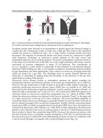
3.2 Asymmetric UWB-RFID architecture
On the basis of the considerations above, we propose an asymmetric UWB-RFID system
architecture illustrated in Figure 5. Due to the nature of the impulse UWB radio, the UWB-
IR transmitter integrated on the RFID tag provides a robust, high speed and high security
uplink under a low power and low complexity implementation. Instead of the typical full-
UWB system, the traditional RF transceiver is applied as the downlink. First, as the
discussion in previous section, in full-UWB system, the wide-band RF receiver consumes too
much power which makes it impossible for tag to be powered wirelessly in battery-less
systems, whereas using battery in tag causes high maintenance cost and big size. Second,
unlike other communication systems, RFID and WSN applications are dominated by uplink
communication, where the low downlink traffic becomes insignificant for the system
efficiency. As a result, the low data-rate narrowband radio is adequate [16, 17].
The reader broadcasts commands to tags using UHF (870MHz ~ 960MHz) signal. The
modulation is ASK with pulse interval encoding (PIE). The data rate (clock frequency) is
adaptive from 40Kbps (KHz) to 160 Kbps (KHz) controlled by the reader. A tag replies
information by transmitting UWB signal with adaptive data-rate up to 10Mbps. The UWB
pulse rate and data–rate are adapted by reader based on the available power and desired
operation distance. In long range operation when the availavle power to the tag is low,
lower pulse rate and data rate is chosen resulting lower power consumption. On the other
Remotely UHF-Powered Ultra Wideband RFID for Ubiquitous Wireless Identification and Sensing
115
hand, in short range applications, higher pulse rate with high data-rate can be transmitted
since the available power is high enough.
In [12], BPSK achieves the best BER performance in the AWGN and Rayleigh fading
channels simulations. However the circuit complexity is the highest and the receiver needs a
coherent system to demodulate data. Thus, this modulation is not suitable for the RFID
implementation. Either OOK or PPM modulation can be used in the tags to modulate the
UWB pulses. Although, OOK modulation has less communication performance however, it
results in simple and low power implementation. Therefore, in this design OOK modulation
is utilized. As can be seen later, UWB pulses are transmitted synchronous with the incoming
RF signal, which brings further simplification in synchronization and improves the
detection performance in readers.
Fig. 5. Proposed system model of asymmetric UWB-RFID architecture
3.3 Data communication protocol
The specification in higher layers is a further issue that determines the energy efficiency as
well as the system throughput. Hereby, we devise a specified data communication protocol
for the proposed asymmetric UWB-RFID architecture. Multi-access is also considered in the
proposed protocol.
3.3.1 Operation procedure
Because of the great asymmetric between reader and tags, the system works in a master-
slaver communication mode. A reader initiates all the operations, followed by tags’
responses. All the calculations are made by the reader and hence the tag implementation is
very simple. Five operations are defined in the proposed protocol, namely Wakeup,
Request, Write, Modify and Kill. The Wakeup and the Request are basic operations for
identifying tags or gathering data. The Wakeup activates and identifies all tags in the
reading field while the Request performs the similar function as the Wakeup, but does not
affect the identified tags. The Write function is for initialization of the tag and the Modify is
used to program a specific tag with access control. The tag can be deleted by using the Kill
function. The frame format, also called round, which represents an operation initiated by
Development and Implementation of RFID Technology
116
readers, is composed by four phases: powering, start of frame (SOF), commands, and
processing. In the powering phase, the reader radiates a continuous sinusoid wave to power
passive tags. A SOF is used for frame synchronization. The sequence consists of ten continuous
bit 0s and a bit 1. Afterwards, tags decode the received command and respond the reader.
An acknowledgement mechanism is employed to guarantee the successful receptions and to
disable the identified tags. Unlike traditional RFID where data integrity (QoS) is controlled
by both readers and tags such as CRC check, in the proposed system, only readers take
charge of error handling. As a result, CRC checker can be removed from a tag which reduces
the complexity. After each operation, the tag sends its current data and the reader checks the
correctness of the operation. Because the uplink speed is high, this approach will not cause
the processing delay even transmitting whole data.
Figure 6 shows the state transition diagram of the main state machine for tags.
Fig. 6. The State Transition Diagram of UWB-RFID Tag
• Powering Up State: Passive tags capture power by the power scavenging units and
store in a relatively big capacitor. This stored energy is used later for transmission.
• Halt/Detecting State: This is the initial state of each powered tag. In this state, tags are
detecting incoming signals and capturing SOF and Command. After this state, tags
enter a new frame to execute the corresponding operation.
• Transmitting State: A tag executes three procedures during transmitting state. First
step is to load data into the cache and generate a PN code. Secondly, a slot counter in
the tag counts down the PN code until it reaches 0. Finally, the tag sends the data and
waits for ACK or NAK.
• Writing State: A tag programs its memory by receiving data from the reader.
• Access State: This state comes before an operation for a specific tag (Modify and Kill
Commands). The tag compares its data with the incoming signals bit by bit. This state is
interrupted by different bits. Only one tag with the same data completes the state.
• Kill State: It sets the Kill Flag to permanently disable the tag.
Remotely UHF-Powered Ultra Wideband RFID for Ubiquitous Wireless Identification and Sensing
117
3.3.2 Anti-collisions
In contrast to conventional wireless system, massive nodes (tags) are deployed in a dynamic
environment. Random access method is applied in our work, rather than current medium
access control (MAC) protocols for UWB-IR including time division multiple access
(TDMA), time hopping, or direct sequence UWB (DS-UWB) [18]. In [19] several versions of
the ALOHA algorithm are presented in order to increase its feasibility and efficiency.
Among them, the most widely used one in wireless sensor and identification systems is the
framed slotted ALOHA algorithm. Time is divided into discrete time intervals, called slots.
A frame is a time interval between requests of a reader and consists of a number of slots. A
tag randomly selects a slot number in the frame and responds to the reader. A procedure
called acknowledgment is required to resolve collisions or failed transmissions. Collided
tags retransmit in the next frame [19].
The overall goal of the anti-collision algorithm is to reduce the identification period with
simple hardware implementation and low power consumption. To improve network
throughput, we propose a more efficient scheme to overcome the anti-collision problem. It is
based on the framed slotted ALOHA algorithm by employing following improvements.
• The pipelined Communication Scheme: In conventional approaches, a time slot
normally contains a tag’s data packet and the acknowledgement from the reader.
However, because there exist great asymmetry between the downlink and the uplink
(UWB data rate is much higher than the narrowband radio data rate), the
acknowledgement from the reader to tags becomes a bottleneck that decreases the
network throughput. This problem can be solved by using a pipelined method that
poses the data packet and its corresponding acknowledgement in two adjacent slots. As
can be seen in Figure 7, a tag sends data in the K slot and receives the ACK in the K + 1
slot. Processing gain in slot is calculated in Eq.2.
(2)
Fig. 7. The sketch of the pipelined communication protocol
Development and Implementation of RFID Technology
118
• Skipping Idle Slots: Because the global clock is scalable controlled by the reader, it
provides a possibility to skip idle slots. By detecting the incoming signals at the
beginning of each slot, the reader can determine if there is any transmission in this time
slot. If it is an idle slot (phase B in Figure 8), the reader skips this slot by adjusting the
clock frequency and transits into the next cycle (slot) immediately.
Fig. 8. Sketch of Idle Slot Skipping
• Adaptive Frame Size: The maximum system efficiency of the framed slotted ALOHA is
achieved when the frame size (N) approximately equals to the tag number (n) [20].
Dynamic frame sizes allocation replaces the traditional fixed framed ALOHA. With the
tag number estimation algorithm [21], the reader can estimate the number of tags, and
optimized the frame size.
Hereby, the system efficiency is defined as the ratio of the successful transmission time to
the frame size. Given N slots and n tags, the number of r of tags in one same slot is
binomially distributed as Eq.3.
(3)
If the frame size is small but the number of tags is large, too many collisions will occur and
the fraction of identified tags will degrade. On the other hand, when the number of tags is
much smaller than the number of slots, the wasted slots can occur. As described the
dynamic frame size allocation can provide the optimal frame size to achieve the maximum
throughput. Moreover, the idle skipping method can eliminate the delay caused by the
empty slots. The simulation results of the system performance are shown in Figure 9. It
demonstrates that more than 2000 tags/s can be processed. Table 2 presents the comparison
result with some standardized RFID protocols.
4. Implementation of the remote-powered UWB-RFID tag
A Remote-Powered UWB-RFID tag is designed for proof of concept and implemented in
UMC 0.18μm process (Figure 10). The module consists of five parts: an RF demodulator, an
impulse UWB transmitter, a power management unit, a clock circuitry, and a digital
baseband. The narrowband receiver receives RF signal and demodulates it into digital
signal. The power management unit captures the incoming RF signal and rectifies to DC
voltage and supplies the whole circuitry of the tag. A low frequency clock is recovered from
the received data as the baseband control. Another high frequency clock for the UWB pulse
generator is imported by dividing the carrier of the incoming signal. The digital baseband is
responsible for control, i.e., decodes commands, programs memory, fetch data, and exports
data to the transmitter.
Remotely UHF-Powered Ultra Wideband RFID for Ubiquitous Wireless Identification and Sensing
119
Fig. 9. Simulation Results of System Performance
Table 1. Comparison of different standardized protocols
Fig. 10. Block diagram of the UWB-RFID Tag
Development and Implementation of RFID Technology
120
4.1 Impulse UWB transmitter
Impulse UWB Transmitter generates 5
th
derivatives Gaussian pulses to modulate the
baseband information into UWB signals. A tunable impulse UWB transmitter is shown in
Figure 11. Duration and amplitude of the output pulse are controlled by two inputs that
have capability to compensate the process and temperature variations, interconnection and
packaging effects, and frequency response of the antenna. Furthermore, this ability allows
the module to control output power and bandwidth in different pulse repetition rates. In
short range applications, high repetition rate and low amplitude pulses are transmitted. On
the contrary, to transmit data in longer distance, low repetition rate and high amplitude
pulses are chosen. In both of two cases, amplitude and duration controls enable the module
to transmit a signal comply the FCC regulation [22, 23]. The output impulse of the UWB
transmitter and its power spectral density are shown in Figure 12. The power consumption
of UWB-Tx at 10 MHz pulse repetition rate is 51 μA at 1.8V, and 252 μA at 50 MHz pulse
repetition rate.
Fig. 11. Schematic of the I-UWB Transmitter
Fig. 12. Output pulse shape of the I-UWB Transmitter and ITS Spectrum
4.2 Power management unit
The power management unit provides power supply for the whole circuitry from incoming
electromagnetic wave. Figure 13 shows the principle of operation. During the powering
Remotely UHF-Powered Ultra Wideband RFID for Ubiquitous Wireless Identification and Sensing
121
phase the Power-Switch is open, and thus the power consumption is very low (1uA). The
power scavenging unit (PSU) converts the received electromagnetic wave to a dc voltage on
an off-chip capacitor. When the voltage across the storage capacitor raises a certain value
(e.g. 2.5V), a voltage sensor (Vsen) switches on the Power-Switch and the chip starts to
operate. While the chip is working, voltage across the storage capacitor is degraded;
therefore a low-dropoutput (LDO) voltage regulator is utilized to provide regulated voltage
for the module. If the voltage becomes less than a threshold (e.g. 1.8V), the voltage sensor
switches off the chip, and chip starts to gather energy for next run [24].
Fig. 13. Operation principle of power management unit
Figure 14 shows the schematics of different building blocks of the power management unit
including of the power scavenging unit, the voltage sensor, and LDO voltage regulator. The
minimum input power of 14.1 μW is achieved with this technique. It corresponds to 13.9
meters operation range which is great improvement compared with conventional RFID.
4.3 RF demodulator
Such as conventional RFID, a simple RF demodulator is utilized. It includes an envelope
detector and a discriminator circuit which extract data and clock from the received signal.
The envelop detector uses the same CMOS voltage multiplier topology than power
scavenging unit, but with smaller capacitors and only 2 stages. The discriminator circuit
decides whether a pulse is long or short and extracts data and clock. Extracted clock is used
as the global clock for baseband control. Figure 15 depicts the schematic of the RF
demodulator including of envelop detector, and clock and data recovery block diagram.
4.4 Clock generator
UWB transmitter requires high frequency clock with low skew and jitter. LC oscillators
occupy large area and consume high power. On the other hand, ring oscillator show large
variation across the process, temperature and voltage as well as huge phase noise [8].
Utilizing the PLLs which are used in communication systems are not applicable in RFID tag
because of their high complexity and power consumption. In this work a low power
harmonic injection locked (HIL) divide-by-3 is used to down convert the 900MHz carrier
frequency [25]. Figure 16 shows the schematic of the divide-by-3 circuit and the output
spectrum before and after locking. Simulation result of the harmonic injection locked
divider shows total power consumption of 15.3μA. The minimum input voltage for locking
is 100mv which is acceptable for this operation range. Phase noise of the output at 10Hz
offset is -85dBc/Hz and jitter is 1.47ps.
Development and Implementation of RFID Technology
122
(a) Power scavenging unit
(b) Voltage sensor
(c) Low-Drop-Out Voltage Regulator
Fig. 14. Schematics of power management unit
Remotely UHF-Powered Ultra Wideband RFID for Ubiquitous Wireless Identification and Sensing
123
Fig. 15. Schematic of RF demodulator
Fig. 16. Schematic of divide-by-3 and output spectrum before and after lock
4.5 Digital control logic
Digital control logic is used for baseband processing, medium access control, and power
management. Figure 17 illustrates the architecture of the processor. The control unit is
formed by several FSMs which generate control signals to each sub module whereas sub
modules send status signals to the control unit. The pseudo number generator (PNG) and
the slot counter are used to implement the transmission protocol and the anticollision
algorithm. The circuit simulation is successful and the design is tested by FPGA prototype.
We also map the design in UMC 0.18um process. The area is equivalent to 4000 NAND
gates and the power consumption is around 800nW [26]
5. Conclusion
In this chapter, a novel system with asymmetric wireless links has been presented for
ubiquitous wireless sensing and identification. Such as conventional passive RFID systems,
nodes derive the power supply and receive data from the received RF signal transmitted by
a reader. However, instead of backscattering, impulse UWB radio technique has been
utilized in uplink from the nodes to the readers. It offers several advantages to the system
such as high throughput, precise ranging and positioning, more security, long operation
range, robustness to multipath, robustness to the narrowband interference and multi user
Development and Implementation of RFID Technology
124
Fig. 17. Block diagram of baseband logic
interference. A new communication protocol is proposed for the novel system with
asymmetric wireless links. It is based on Frame Slotted ALOHA anti-collision algorithm.
Dynamic frame size allocation and idle slot skipping methods are investigated and the
performance simulation results show a throughput more than 2000 tags per second for the
system which great improvement compared to the conventional RFID systems (at most 1000
tags/s). To proof of the concept, a complete module for the tag has been implemented in
0.18 μm CMOS process. The measurement results shows the operation distance of 14 meters
when 4W EIRP emission is allowed at 900 MHz frequency band. The impulse UWB
transmitter consumes 51 μA at 10 MHz pulse rate which is low enough to be provided by
the power management unit for 1.9 millisecond time. The results proof the validity of the
proposed concept and show the great potential of impulse UWB radio for next generation of
RFID for ubiquitous wireless sensing.
6. References
[1] "The Internet of Things," International Telecommunication Union (ITU) Internet Report
2005.
[2] K. Finkenzeller, RFID-Handbook: Fundamentals and Applications in Contactless Smart
Cards and Identification, 2nd ed.: Wiley & Sons LTD 2003.
[3] R. Want, "Enabling ubiquitous sensing with RFID," Computer, vol. 37, pp. 84-86, 2004.
[4] J. Guang-yao, L. Xiao-yi, and P. Myong-Soon, "An Indoor Localization Mechanism Using
Active RFID Tag," in Sensor Networks, Ubiquitous, and Trustworthy Computing, 2006.
IEEE International Conference on, 2006, pp. 40-43.
[5] D. S. Ha and P. R. Schaumont, "Replacing Cryptography with Ultra Wideband (UWB)
Modulation in Secure RFID," in RFID, 2007. IEEE International Conference on, 2007,
pp. 23-29.
Remotely UHF-Powered Ultra Wideband RFID for Ubiquitous Wireless Identification and Sensing
125
[6] X. Duo, T. Torikka, Z. Li-Rong, M. Ismail, H. Tenhunen, and E. Tjukanoff, "A DC-13GHz
LNA for UWB RFID applications," in Norchip Conference, 2004. Proceedings, 2004, pp.
241-244.
[7] F. U. Dowla, "Long-Range Ultra-Wideband Radio-Frequency Identification," LLNL
Engineering 2004.
[8] L. Stoica, A. Rabbachin, H. O. Repo, T. S. Tiuraniemi, and I. Oppermann, "An
ultrawideband system architecture for tag based wireless sensor networks,"
Vehicular Technology, IEEE Transactions on, vol. 54, pp. 1632-1645, 2005.
[9] N. Patwari, J. N. Ash, S. Kyperountas, A. O. Hero, III, R. L. Moses, and N. S. Correal,
"Locating the nodes: cooperative localization in wireless sensor networks," Signal
Processing Magazine, IEEE, vol. 22, pp. 54-69, 2005.
[10] J. H. Reed, An Introduction to Ultra Wideband Communication Systems: Prentice Hall
PTR, 2005.
[11] FCC, "First report and order," Available online
attachmatch/FCC-02- 48A1.pdf, 2002.
[12] I. Guvenc and H. Arslan, "On the modulation options for UWB systems," in Military
Communications Conference, 2003. MILCOM 2003. IEEE, 2003, pp. 892-897 Vol.2.
[13] K. Siwiak and D. McKeown, Ultra Wideband Radio Technology: John Wiley & Sons Ltd,
2004.
[14] I. Oppermann, L. Stoica, A. Rabbachin, Z. Shelby, and J. Haapola, "UWB wireless sensor
networks: UWEN – a practical example," Communications Magazine, IEEE, vol. 42,
pp. S27-S32, 2004.
[15] "
[16] M. Baghaei Nejad, Z. Zou, H. Tenhunen, and L R. Zheng, "A Novel Passive Tag with
Asymmetric Wireless Link for RFID and WSN Applications," in Circuits and
Systems, 2007. ISCAS 2007. IEEE International Symposium on, 2007, pp. 1593-1596.
[17] M. Baghaei Nejad, Z. Zou, D. S. Mendoza, H. Tenhunen, and L R. Zheng, "Enabling
UbiquitousWireless Sensing by a Novel RFID-Based UWB Module," in First
International EURASIP Workshop on RFID Technology, Vienna, Ausria, 2007.
[18] R. Scholtz, "Multiple access with time-hopping impulse modulation," in Military
Communications Conference, 1993. MILCOM '93. Conference record.
'Communications on the Move'., IEEE, 1993, pp. 447-450 vol.2.
[19] ETH, "RFID Multiple Access Methods," Zurich 2004.
[20] L. Su-Ryun, J. Sung-Don, and L. Chae-Woo, "An enhanced dynamic framed slotted
ALOHA algorithm for RFID tag identification," in Mobile and Ubiquitous Systems:
Networking and Services, 2005. MobiQuitous 2005. The Second Annual International
Conference on, 2005, pp. 166-172.
[21] C. Jae-Ryong and K. Jae-Hyun, "Novel anti-collision algorithms for fast object
identification in RFID system," in Parallel and Distributed Systems, 2005. Proceedings.
11th International Conference on, 2005, pp. 63-67 Vol. 2.
[22] S. M. David, M. Baghaei-Nejad, H. Tenhunen, and L R. Zheng, "Low Power Tunable
CMOS I-UWB Transmitter Design," in IEEE 2007 Norchip, 19-20 November 2007,
Aalborg, Denmark, 2007.
[23] M. Baghaei Nejad, H. Tenhunen, and L R. Zheng, "Chip-Package and Antenna Co-
Design of a Tunable UWB Transmitter in System-on-Package with On-Chip versus
Development and Implementation of RFID Technology
126
Off-Chip Passives," in Electronics Systemintegration Technology Conference, 2006. 1st,
2006, pp. 291-298.
[24] M. Baghaei Nejad, H. Tenhunen, and L R. Zheng, "Power Management and Clock
Generator for a Novel Passive UWB Tag," in System-on-Chip, 2007 International
Symposium on, Tampere, Finland, 2007, pp. 82-85.
[25] M. Motoyoshi and M. Fujishima, "43μW 6GHz CMOS Divide-by-3 Frequency Divider
Based on Three-Phase Harmonic Injection Locking," in Solid-State Circuits
Conference, 2006. ASSCC 2006. IEEE Asian, 2006, pp. 183- 186.
[26] Z. Zou, M. Baghaei Nejad, H. Tenhunen, and L R. Zheng, "Baseband Design for Passive
Semi-UWB Wireless Sensor and Identification Systems," in IEEE International SoC
Conference SoCC 07, 2007.
7
Development of Sensing and Computing
Enhanced Passive RFID Tags Using the
Wireless Identification and Sensing Platform
Alanson Sample
1,2
, Daniel Yeager
1
, Michael Buettner
1
and Joshua Smith
2
1
University of Washington,
2
Intel Research Seattle
USA
1. Introduction
Passive RFID tags are becoming increasingly common in home and work environments. As
RFID tags find new applications beyond shipment tracking, they are being embedded in
objects throughout our environment. RFID tags are already being incorporated in credit
cards for touch-free payments, in clothing for merchandise tracking, and in ID cards for
building access control.
All these “non-shipping” RFID tags are powered wirelessly and are capable of wireless
communication and rudimentary computation. Thus they can be viewed as micro-
computing platforms with wireless power and communication capabilities. While the
functionality of today’s passive RFID tags is extremely limited, today’s tags can already be
thought of as a layer of invisible computing that is seamlessly embedded in objects
throughout the environment. This primitive layer of embedded intelligence could grow in
sophistication if additional sensing and computation capabilities could be added to RFID
tags.
The authors’ goal is to evolve this layer of passively powered embedded intelligence by
creating RFID tags that support sensors and can execute general purpose computer
programs. This chapter reviews several years’ work on the development of our open,
programmable passive RFID tag, the Wireless Identification and Sensing Platform (WISP).
It also shows how to use the EPC Class 1 Generation 2 RFID protocol to implement
advanced RFID sensing applications that go far beyond simple tag ID inventorying
applications.
Our first venture into sensor-enhanced RFID was the α-WISP shown in Figure 1 (Philipose
et al., 2005). With this device, one bit of sensor data was encoded by using anti-parallel tilt
switches to multiplex one of two RFID tag ICs to a single antenna. Thus, a reader could infer
three states about a tagged item (tag right side up, upside down, or not present). This simple
example of overloading the EPC ID to encode sensor data allowed inference of very coarse
orientation information. However, the use of commercial RFID tag ICs restricted our ability
to control the RFID communication channel and in turn our ability to configure WISPs for
new applications.
Development and Implementation of RFID Technology
128
Fig. 1. The α-WISP uses two tilt switches orientated in opposite directions as a simple one bit
RFID accelerometer.
In order to fully investigate passive RFID applications, we developed the general purpose
Wireless Identification and Sensing Platform (simply called WISP) (Sample et al., 2008).
Shown in Figure 2, the WISP is a battery-free, programmable RFID sensor device. Compliant
with the Electronic Product Code (EPC) Class 1, Generation 2 protocol, the WISP can
transmit multiple bytes of data per query and is fully configurable due to its ultra-low
power 16-bit general-purpose microcontroller. Similar to conventional passive UHF RFID
tags, the WISP has no batteries and is completely powered via the RF energy transmitted by
an RFID reader.
The architecture of the WISP allows measurement of virtually any low power sensor which
can also be wirelessly powered by the RFID reader. The WISP is implemented as a printed
circuit board (PCB), which offers a flexible platform for exploring new sensor integration
schemes and applications. To the authors’ knowledge, the WISP is the first passive UHF
RFID tag with an integrated microcontroller and has an operating range of several meters.
Fig. 2. Wireless Identification and Sensing Platform (WISP)
The first few section of this chapter presents an overview of the WISP platform including a
detailed explanation of the architecture and power management algorithm. In particular,
performance metrics describing operational range and real world performance are
presented. Section 5 presents an over view of how the Electronic Product Code (EPC)
Generation 2 Class 1 protocol is used to create a bi-directional communication channel for
sending data to and from the a RFID reader. Section 6 explores the application space of the
Development of Sensing and Computing Enhanced Passive RFID Tags
Using the Wireless Identification and Sensing Platform
129
WISP. This platform is intended to be a vehicle with which researchers can quickly
investigate new and innovative applications in RFID. To highlight this concept several case
studies of recent applications using the WISP are presented; for example, using the WISP to
increase the security of RFID systems, and as a passive data logging device.
2. Prior work
To date there are several approaches to enhancing RFID tags with sensing capabilities. One
method is to use standard commercial tag ICs and alter their functionality to transmit sensor
data, as was done in the case of the α-WISP. The authors in (Johan et al., 2007) describe a
humidity sensor for detecting moisture in walls of buildings and houses by placing a sponge
in front of a tag. Moisture in the sponge detunes the tag’s antenna, allowing the
approximation of humidity levels from the read range of the tag. Another approach uses a
custom tag with a built in fuse for sensing high temperatures in food products. The fuse
melts above a particular threshold which enables or disables the tag (Watters et al., 2002).
These passive tags based on physical properties are extremely limited in what they can
report and are not reusable.
Other efforts have been made to retrieve richer, multi-bit sensor data from RFID tags for a
wide variety of applications. Possible applications include infrastructure and object
monitoring, automatic product tamper detection, identification of harmful agents, and
biomedical devices for noninvasive monitoring (Want, 2004). To enable these applications
two regimes have been explored: active battery-powered tags and passive battery-free tags.
Active tags, a subclass of RFID, are essentially wireless sensor nodes (Polastre & Szewczyk,
2005) (Savi Technology, 2006). They use batteries to power their communication circuitry,
sensors, and microcontroller. Active tags benefit from a relatively long wireless range
(approximately 30 m) and can achieve high data and sensing rates. An active tag with
adaptive analog sensor thresholds for triggering sensor measurements was proposed in
(Malinowski, et al., 2007). However, these devices require batteries which are a drawback
when considering the cost, weight and volume of the device, and the need to replace the
dead batteries.
In contrast, passive sensor tags receive their operating energy from the RFID reader which
gives them a life time of years, if not decades. Examples of application-specific, non-
programmable UHF passive tags with integrated temperature and light sensors, as well as
an Analog to Digital Converter (ADC) can be found in (Namjun et al., 2005) and (Kocer &
Flynn, 2006). One attractive feature of passive sensor tags is the prospect of permanently
embedding them in objects for structural, medical, or product monitoring. Another
advantage is their suitability for applications in which neither batteries nor wired
connections are feasible, for weight, volume, cost, or other reasons. Of course, the limitation
of purely passive sensor tags is the requirement of proximity to an RFID reader. However,
methods such as solar, thermal, or kinetic energy harvesting could be used as a secondary
power source if needed.
A further consideration is the configurability and computational power of RFID sensor tags.
Existing devices are generally fixed-function with respect to sensory inputs and lack
computational capabilities. A commercially available RFID tag with limited additional
functionality is described in (Microchip Technology Inc, 2005); however, this device can only
transmit one bit of sensor data in addition to its ID. Furthermore, it is limited by a short read
range due to its 125 kHz operating frequency.
Development and Implementation of RFID Technology
130
3. WISP architecture
The WISP is manufactured as a printed circuit board (PCB) which offers a number of
advantages compared to traditional Integrated Circuit (IC) tag designs. Primarily low
development cost, fast design cycles, and easy debugging and measurement of circuit
parameters. The PCB implementation allows the flexibility to physically add and remove
sensors and/or peripherals to create devices for new applications. In contrast, IC
implementations offer the ability to customize components and decrease power
consumption (yielding better range), as well as creating devices with a smaller form factor
and at a lower cost when manufactured in high volume.
A block diagram of the WISP is shown in figure 2 and is similar in function to traditional IC
RFID tags. The antenna is balanced by an impedance matching network and is fed into the
RF power harvester. The Radio Frequency (RF) signal transmitted by the RFID readers is
rectified into DC power to power the rest of the tag. The demodulator block converts the
Phase-Reversed Amplitude Shift Keyed (PR-ASK) data that is superimposed on the RF
carrier into a logic level steam of serial data. This extracted serial data is parsed by the
MSP430 microcontroller (MCU) to receive downlink data from the reader. Uplink data is
sent via the modulator circuit, which “back-scatters” the signal by changing the antenna
impedance. Finally, the microcontroller’s internal temperature sensor, as well as any
external sensors, are powered and measured by the MCU.
As the power consumption of the microcontroller, sensors, and peripherals are much greater
then that seen in traditional passive RFID technology, the WISP duty cycles between active
and sleep mode. In sleep mode, the WISP shuts down and reduces its current consumption
to a few micro-amps and energy is accumulated by the harvester block over multiple EPC
queries. Once sufficient voltage is obtained, the WISP polls sensors and communicates with
the RFID reader.
Fig. 3. Block Diagram of the WISP
Figure 3 depicts the WISP platform, made of a four layer FR4 PCB with components on both
sides and an integrated dipole antenna. The WISP in its base configuration has several
onboard sensors: a circuit for measuring the rectified supply voltage, a temperature sensor,
and a 3D accelerometer. Small header pins expose all ports of the microcontroller for
expansion to daughter boards, external sensors, and peripherals. Finally, a low current
surface mount LED is included in the design.
Development of Sensing and Computing Enhanced Passive RFID Tags
Using the Wireless Identification and Sensing Platform
131
3.1 RF power harvesting
The defining characteristic of far field RFID systems is that tags can be read at a significant
distance, generally on the order of 2-10 meters. For passive RFID this requires that the RFID
reader transmits sufficient energy to power the tag at large distances. However, due to
regulatory limits on the amount of power that can be transmitted and the path loss
associated with electromagnetic propagation, there is very little power that actually reaches
the tags. Therefore, the power harvesting circuit must maximize the operating distance by
converting the very limited incoming RF power to DC power with sufficient voltage to
activate the tag.
The RF power received by the WISP’s dipole antenna is fed to the analog front end depicted
in figure 4. A discrete matching network is used to provide the maximum power transfer
from the antenna to the rectifier. RF Schottky diodes specifically designed for 915MHz low
power application were selected to make a five-stage voltage doubling circuit. This circuit
converts the AC input signal to DC power which is fed into a storage capacitor.
RF Rectifier
+
-
LS
Voltage
Regulator
(1.8v)
Voltage
Supervisor
(1.9v)
Power Management
Demodulator
Vreg
Vreg
POR = 1.6v
Wake Up
Received
Data Enable
Received Data
Rectified DC Power
Stored Voltage
RF input
Fig. 4. Schematic of the Analog Front End
For RF rectifiers of this type, the input and output impedances are not well isolated. Further
confounding the problem is that the output impedance of the rectifier is fairly high; an
undesirable trait for any power source. This means that as the load on the rectifier changes
the input impedance also changes, resulting in the analog front end becoming mismatched
to the antenna. This leads to the problem of selecting values for the impedance matching
network when it is not possible to guarantee constant input impedance.
To determine the correct values for the matching network the operating cycle of the WISP
must be taken into account. First, the WISP is most effective at storing harvested energy
when it is in sleep mode, as the current consumption is minimal. Second, the WISP will
spend most of its time repeatedly charging up to 1.9v and then discharging to
approximately 1.8v. Thus, to determine the correct values the WISP is put in sleep mode and
Development and Implementation of RFID Technology
132
we find the impedance matching network that produces 1.9v for the lowest possible input
power. Stated another way, the key parameter for maximizing the read distance of the WISP
is minimizing the quiescent current consumption so that the minimum operating voltage of
1.9V (supervisor threshold) can be rectified with the lowest possible input power.
To characterize the system, a network analyzer was used to inject a continuous 915 MHz
waveform into the antenna ports of the WISP. Using the minimum input power needed for
activation, the expected operating distance for the WISP can be calculated with the
logarithmic form of the Friis path loss equation (1), with a term for polarization mismatch
included.
PRTTR
LGG
d
PP −++
⎟
⎠
⎞
⎜
⎝
⎛
−=
λ
π
4
log20
(1)
The transmit power of the reader P
T
= 1 W = 30 dBm. Its center frequency is 915 MHz,
corresponding to a wavelength (λ) of = 0.33 m. The transmit antenna gain G
T
= 6 dBi (this
yields an effective isotropic radiated power (EIRP) of 4 W, the United States regulatory limit
for this ISM band). The receive antenna gain G
R
= 2 dBi (the standard gain figure for a
dipole antenna), and the polarization loss L
P
= 3dB. Loss L
P
occurs because only half of the
power transmitted from the circularly-polarized transmit antenna is received by the
linearly-polarized receive dipole antenna. Using the experimentally determined operating
thresholds of -9.5 dBm, equation 1 predicts a maximum operational range of 4.3m.
It should be noted that practical implementation of the WISP yields an operating range of
approximately 3 meters. There are a number of contributing factors: the WISP antenna gain
used in equation 1 is estimated not measured, and in the above experiment a continuous
915MHz signal was injected and the storage capacitor was charge to its steady state. Real
RFID systems send out bursts of packets (power and data) with long periods of no signal
between them. In this case the discharge rate of the storage capacitor must be taken into
account. Finally, as with any far field RFID system, constructive and destructive interference
due to multi-path plays a large role in real world results.
3.2 Demodulation and modulation
The EPC Gen 2 standard defines that reader-to-tag communication uses ASK modulation on
a carrier wave in the range of 902-928 MHz. When not transmitting data the carrier
waveform remains at a constant amplitude; when bits are transmitted, the amplitude of the
carrier drops to at least ten percent of its normal value and the phase of the carrier may be
reversed. The duration of the continuous waveform between these low amplitude pulses
indicates logical “ones” or “zeros.”
Figure 3 shows a schematic of the WISP’s demodulator circuit. The output of the harvester is
fed through the diode, which supplies power to the comparator and acts as a reference for
the level shifter. A capacitor is used to filter out transients while allowing proper biasing at
varying distance and receive power levels. When activated, the current consumption of the
comparator functions as a constant-current source, pulling current through the diode. In this
way, the voltage drop across the diode is used as a detector, where current supplied by the
harvester (high amplitude RF modulation) results in positive voltage, and a lack of current
(low amplitude RF modulation) yields negative voltage. The comparator is used to generate
a rail-to-rail logic level waveform, and the level shifter converts the unregulated logic level
to the regulated logic level. It is important to optimize current consumption and speed when
Development of Sensing and Computing Enhanced Passive RFID Tags
Using the Wireless Identification and Sensing Platform
133
choosing a comparator. Further savings can be achieved by disabling the comparator when
there is insufficient voltage to start up the MSP430.
Passive RFID tags do not actively transmit radio signals. Instead, they modulate the
impedance of their antenna which causes a change in the amount of energy reflected back to
the reader. This modulated reflection is referred to as back-scatter radiation. To change the
impedance of the antenna a transistor is placed between the two branches of the dipole
antenna. When the transistor conducts current, it short-circuits the two branches of the
antenna which changes the antenna impedance; in the non-conducting state the transistor
has no effect on the antenna, and thus the power harvesting and data downlink function as
if it were not present.
3.3 Digital section and power conditioning
As the power available to RFID tags is extremely limited, careful component selection is
critical to minimize current consumption. With advances in IC manufacturing that allow
discrete components with current consumption in the range of 1 µA and operation at 1.8 V,
it is now possible to construct functional, wirelessly powered RFID tags with discrete
components.
The general purpose computation capability of the WISP is provided by an ultra low power
microcontroller. This 16-bit flash microcontroller, the MSP430F2272, can operate at up to 4
MHz with a 1.8 V supply voltage and consumes approximately 600 µA when active at this
frequency and voltage. Of particular interest for low power RFID applications, the MSP430
has a number of low power modes. Its minimum RAM-retention supply current is 0.1 µA at
1.5 V. The device provides over 8 kilobytes of flash memory, 256 bytes of RAM and a 10-bit,
200 kilo-samples-per-second Analog to Digital Converter (ADC). The low power
consumption of this device is a critical factor in enabling a general purpose microcontroller
in passive RFID systems.
Another critical design consideration is operation with uncertain power supply conditions.
Because the available RF power varies greatly during device operation, supervisory circuitry
is necessary to wake and sleep the device based on the supply voltage level. The WISP uses
a 1.9 V supervisor and a 1.6 V power-on-reset to control device state and reset the
microcontroller, respectively. The supervisor provides roughly 100 mV of headroom on the
large storage capacitor above the 1.8 V regulator voltage. This serves to buffer the supply
voltage from dropping below 1.8 V due to the large power consumption of the
microcontroller in active mode.
4. Low level firmware and power management algorithm
The WISP is essentially a software defined RFID tag which uses the MSP430 to implement
the EPC Gen 2 Class 1 protocol and performs sensing and computation tasks. There are
significant challenges when developing applications on the WISP as compared to battery
powered embedded systems. Primarily, there is no guarantee that a given task can be
completed before running out of power. Although the voltage supervisor provides
headroom above 1.8 V, the rate at which the energy stored in the supply capacitor is
consumed is directly affected by the design choices of the programmer. Failure to properly
manage sleep cycles, when the WISP harvests energy, or inefficient coding practices can
result poor performance.
Development and Implementation of RFID Technology
134
The WISP software can be described on three levels. At the lowest level is the power
management algorithm which is responsible for managing the device state, including sleep
vs. active modes. Built on that is the communication layer, which enables bi-directional
communication by sampling downlink data bits, implementing a Gen 2 state machine, and
generating uplink data bits. The third level is the application layer where users implement
costume function and encoding data in the appropriate EPC packets.
4.1 Power management algorithm
Meeting the low power requirements of passive RFID tags requires that the MCU consumes,
on average, as little power as possible. As mentioned previously, this is achieved by duty
cycling between active and low power sleep states. The key is that the WISP receives a
constant amount of power as defined by Friis path loss equation 1 for a set distance. When
the WISP is in active mode the power consumption far exceeds the power harvested.
However, when the WISP is in sleep mode the total current consumption of all the circuits is
a few micro-amps and there is a net power gain which charges the storage capacitor.
Therefore, duty cycling does not simply yield lower power consumption; it represents two
different states, power harvesting and active operation.
The state diagram for the power management layer is shown in figure 5. State transitions are
primarily driven by hardware interrupts from the voltage supervisor, which indicate if there
is sufficient energy stored for operation. Initially the WISP is way from a RFID reader and is
in a power down state. When the WISP is brought with in range of a reader it begins to
harvest power and the voltage on the storage capacitors begins to rise. At approximately 1.6
V the MSP430 powers up in a reset state and begins executing code. Since this event is not
driven by the supervisor it is important to enter sleep mode (LMP4) as quickly as possible in
order to avoid browning out and thrashing on start up. Once in LMP4 the WISP waits for
sufficient voltage (1.9 V) as indicted by the supervisor interrupt. Next, the state machine
transitions to the application layer which performs user defined functions such as sensor
measurements. Here an EPC packet is generated and the WISP sets up and waits from a
commutation interpret which indicates the beginning of an EPC packet. In the
communication layer the WISP processes the incoming data, executes the EPC Gen 2
protocol and transmits its response. While not shown in figure 5, the communication layer
often reports the same date twice to increase communication reliability.
4.2 Communication and application layers
A considerable challenge when programming the MSP430 involves meeting the timing
constraints of the EPC protocol while still maintaining a low clock frequency. RFID tags that
have custom state machines are designed at the hardware level to receive and send using
the EPC protocol. The general-purpose MSP430 must be carefully tuned to perform EPC
communication, both for receiving and transmitting data. In particular, a mix of C and
assembly language is used where the C code maintains ease of configurability for the
firmware for different sensor applications and the assembly code allows fine-grained control
of the timing of the MSP430 for EPC communication.
As previously described, the demodulator envelopes and thresholds the Phase-Reversed
Amplitude Shift Keyed (PR-ASK) signal from the reader into a serial date stream
representing the data bits 1 and 0 as long and short pulses, respectively. To interpret data
from the reader, the MSP430 uses the periodic edge of the waveform as a hardware
Development of Sensing and Computing Enhanced Passive RFID Tags
Using the Wireless Identification and Sensing Platform
135
Fig. 5. Power Management Algorithm
interrupt, and then during the interrupt service routine re-samples the bit line to detect a 1
or 0 during the differentiated part of the waveform. This data is quickly shifted into memory
before repeating this process. To detect the end of a transmission, a timer is refreshed during
each bit. When bits are no longer received the timer expires, the packet is interpreted and, if
appropriate, a response is sent to the reader. A detailed description of how the WISP uses
and implements the EPC specification is described in section 5.
Figure 6 shows a set of EPC queries and responses along with the charge/discharge cycle of
the WISP. Since the operating range of the WISP occurs between 1.9v-1.8v the rectified
voltage appears to be nearly constant. In actually the WISP enters active mode at 1.9v,
consumes the energy in the storage capacitor till ~1.8v, then enters a sleep state and harvests
power until 1.9v is reached. This duty cycling can be seen in the packet transmitted plot.
Here the WISP does not to responded to every packets sent by the reader, instead it spends
most of its time in a sleep state.
Performing application level tasks such as sensor measurement is generally done in tight
conjunction with the EPC protocol. In this scenario the completion of a receive/transmit
cycle triggers the application layer to immediately take a sensor measurement, generator the
desired EPC packet and setup for a Query. This protocol centric approach works well for
sensor driven applications where data is requested from the RFID tag at regular intervals.
However, applications which leverage the wirelessly powered computing capability of the
WISP benefit from a loose coupling with the communication layer.
5. EPC class 1 generation 2 collecting sensor data
The Gen 2 MAC protocol used by the WISP provides primitives that can be used for
gathering sensor data and transmitting queries. In this section, we give an overview of the
Gen 2 protocol and discuss these primitives and their limitations.