Wave Propagation 2010 Part 4 docx
Bạn đang xem bản rút gọn của tài liệu. Xem và tải ngay bản đầy đủ của tài liệu tại đây (1.16 MB, 30 trang )
Wave Propagation
82
[4] M. M. Sigalas, C. T. Chan, K. M. Ho, and C. M. Soukoulis, Phys. Rev. B 52, 11 744 ,
(1995).
[5] J. S. McCalmont, M. M. Sigalas, G. Tuttle, K. M. Ho, and C. M. Soukoulis, Appl. Phys.
Lett. 68, 2759, (1995).
[6] Arafa H Aly and Sang-Wan Ryu, J. of Computational and Theoretical Nannoscience, Vol
5, 1-15, (2008).
[7] Arafa H Aly, Materials Chemistry and Physics, 115, 391, (2009).
[8] Arafa H. Aly, Heng-Tung Hsu, Tzong-Jer Yang, Chien-Jang Wu, and C-K Hwangbo, J. of
Applied Physics, 105, 083917,(2009).
[9] John D. Joannopoulos,Steven G. Johnson,Joshua N. Winn,and,Robert D. Meade, Photonic
crystals moleding the flow of light. 2
nd
Edition. Princeton University Press, (2008).
[10] J.D. Joannopoulos, R.D. Meade, J.N. Winn, Photonic Crystals: Molding the Flow of
Light, Princeton University Press, Princeton, NJ, 1995.
[11] Z. Sun, Y.S. Jung, H.K. Kim, Appl. Phys. Lett. 83,3021 (2003); Z. Sun, H.K. Kim, Appl.
Phys. Lett. 85, 642 (2004).
[12] V. Kuzmiak, A.A. Maradudin, Phys. Rev. B 55,7427 (1997).
[13] C J.Wu, M S. Chen, T J. Yang, Physica C 432,133 (2005).
[14] C.H. Raymond Ooi, T.C. Au Yeung, C.H. Kam, T.K. Lam, Phys. Rev. B 61 5920 (2000).
[15] M. Ricci, N. Orloff, S.M. Anlage, Appl. Phys. Lett. 87,034102 (2005).
[16] H.A. Macleod, Thin-Film Optical Filters, 3rd ed., Institute of Publishing, Bristol, 2001,
(Chapter 7).
[17] P. Yeh., “Optical Waves in Layered Media”, J. Wiley a& Sons, Inc., Hoboken, New
Jersey, (2005).
[18] M Bom ,Wolf E, Principles of optics, Cambridge, London,( 1999).
[19] Van Duver.T.,Tumer C.W, Princibles of Superconductor Devices and Circuits, Edward
Arnold,London,(1981)
[20] Hung-Ming Lee, and Jong-Ching Wu, J. Appl. Phys. 107, 09E149 (2010) .
1. Introduction
Photonic crystals are media with a spatially periodical dielectric function (Yablonovitch, 1987;
John, 1987; Joannopoulos et al., 1995; 2008). This periodicity can be achieved by embedding
a periodic array of constituent elements with dielectric constant ε
1
in a background
medium characterized by dielectric constant ε
2
. Photonic crystals were first discussed by
Yablonovitch (Yablonovitch, 1987) and John (John, 1987). Different materials have been used
for the corresponding constituent elements including dielectrics (Joannopoulos et al., 1995;
2008), semiconductors, metals (McGurn & Maradudin, 1993; Kuzmiak & Maradudin, 1997),
and superconductors (Takeda & Yoshino, 2003; Takeda et al., 2004; Berman et al., 2006; Lozovik
et al., 2007; Berman et al., 2008; 2009). Photonic crystals attract the growing interest due to
various modern applications (Chigrin & Sotomayor Torres, 2003). For example, they can be
used as the frequency filters and waveguides (Joannopoulos et al., 2008).
The photonic band gap (PBG) in photonic crystals was derived from studies of
electromagnetic waves in periodic media. The idea of band gap originates from solid-state
physics. There are analogies between conventional crystals and photonic crystals. Normal
crystals have a periodic structure at the atomic level, which creates periodic potentials for
electrons with the same modulation. In photonic crystals, the dielectrics are periodically
arranged and the propagation of photons is largely affected by the structure. The properties
of the photons in the photonic crystals have the common properties with the electrons in the
conventional crystals, since the wave equations in the medium with the periodic dielectric
constant have the band spectrum and the Bloch wave solution similarly to the electrons
described by the Schr
¨
odinger equation with the periodic potential (see (Berman et al., 2006)
and references therein). Photonic crystals can be either one-, two- or three-dimensional as
shown in Fig. 1.
In normal crystals there are valence and conduction bands due to the periodic field. Electrons
cannot move inside the completely filled valence band due to the Pauli exclusion principle
for electrons as fermions. Electrons can move inside the crystal if they are excited to the
Oleg L. Berman
1
, Vladimir S. Boyko
1
,
Roman Ya. Kezerashvili
1,2
and Yurii E. Lozovik
3
1
Physics Department, New York City College of Technology,
The City University of New York, Brooklyn, NY 11201
2
The Graduate School and University Center,
The City University of New York, New York, NY 10016
3
Institute of Spectroscopy, Russian Academy of Sciences, 142190 Troitsk
1,2
USA
3
Russia
Electromagnetic Wave Propagation in
Two-Dimensional Photonic Crystals
5
2 Electromagnetic Waves
Fig. 1. Example of 1D, 2D and 3D photonic crystals. All of the photonic crystals shown above
have two different dielectric media. (a) 1D multilayer; (b) 2D array of dielectric rods; (c) 3D
woodpile.
conduction band. Because the photons are bosons, all bands in the photonic crystals’ band
structure are conduction bands. If the frequency corresponds to the allowed band, the photon
can travel through the media. If the photonic gap exists only in the part of Brillouin zone,
then this gap corresponds to the stop band. By other words, photons cannot propagate with
frequencies inside the gap at the wavevectors, where this gap exists. Of particular interest
is a photonic crystal whose band structure possesses a complete photonic band gap. A PBG
defines a range of frequencies for which light is forbidden to exist inside the crystal.
The photonic crystals with the dielectric, metallic, semiconductor, and superconducting
constituent elements have different photonic band and transmittance spectra. The dissipation
of the electromagnetic wave in all these photonic crystals is different. The photonic crystals
with the metallic and superconducting constituent elements can be used as the frequency
filters and waveguides for the far infrared region of the spectrum, while the dielectric photonic
crystals can be applied for the devices only for the optical region of the spectrum.
In this Chapter we discuss the photonic band structure of two-dimensional (2D) photonic
crystals formed by dielectric, metallic, and superconducting constituent elements and
graphene layers. The Chapter is organized in the following way. In Sec. 2 we present the
description of 2D dielectric photonic crystals. In Sec. 3 we review the 2D photonic crystals
with metallic and semiconductor constituent elements. In Sec. 4 we consider the photonic
band structure of the photonic crystals with the superconducting constituents. A novel type
of the graphene-based photonic crystal formed by embedding a periodic array of constituent
stacks of alternating graphene and dielectric discs into a background dielectric medium is
studied in Sec. 5. Finally, the discussion of the results presented in this Chapter follows in
Sec. 6.
2. Dielectric photonic crystals
The 2D photonic crystals with the dielectric constituent elements were discussed in
Ref. (Joannopoulos et al., 2008). Maxwell’s equations, in the absence of external currents and
sources, result in a form which is reminiscent of the Schr
¨
odinger equation for magnetic field
H
(r) (Joannopoulos et al., 2008):
∇×
1
ε(r)
∇×
H(r)
=
ω
c
2
H(r) , (1)
where ω is the frequency of the electromagnetic wave, c is the speed of light, ε
(r) is the
dielectric constant, which is the periodic function of the radius vector in the photonic crystal.
Eq. (1) represents a linear Hermitian eigenvalue problem whose solutions are determined
entirely by the properties of the macroscopic dielectric function ε
(r). Therefore, for a crystal
84
Wave Propagation
Electromagnetic Wave Propagation in Two-Dimensional Photonic Crystals 3
Fig. 2. Frequencies of the lowest photonic bands for a triangular lattice of air columns
(ε
air
= 1) drilled in dielectric (ε = 13). The band structure is plotted along special directions of
the in-plane Brillouin zone (k
z
= 0), as shown in the lower inset. The radius of the air
columns is r
= 0.48a, where a is the in-plane lattice constant. The solid (dashed) lines show
the frequencies of bands which have the electric field parallel (perpendicular) to the plane.
Notice the PBG between the third and fourth bands.
consisting of a periodic array of macroscopic uniform dielectric constituent elements, the
photons in this photonic crystal could be described in terms of a band structure, as in the
case of electrons. Of particular interest is a photonic crystal whose band structure possesses a
complete photonic band gap.
All various kinds of 2D dielectric photonic crystals were analyzed including square,
triangular, and honeycomb 2D lattices (Joannopoulos et al., 2008; Meade et al., 1992).
Dielectric rods in air, as well as air columns drilled in dielectric were considered. At the
dielectric contrast of GaAs (ε
= 13), the only combination which was found to have a PBG
in both polarizations was the triangular lattice of air columns in dielectric. Fig. 2 (Meade et
al., 1992) represents the eigenvalues of the master equation (1) for a triangular lattice of air
columns (ε
air
= 1) drilled in dielectric (ε = 13).
The photonic band structure in a 2D dielectric array was investigated using the coherent
microwave transient spectroscopy (COMITS) technique (Robertson et al., 1992). The array
studied in (Robertson et al., 1992) consists of alumina-ceramic rods was arranged in a regular
square lattice. The dispersion relation for electromagnetic waves in this photonic crystal was
determined directly using the phase sensitivity of COMITS. The dielectric photonic crystals
can be applied as the frequency filters for the optical region of spectrum, since the propagation
of light is forbidden in the photonic crystal at the frequencies, corresponding to the PBG,
which corresponds to the optical frequencies.
3. Photonic crystals with metallic and semiconductor components
The photonic band structures of a square lattice array of metal or semiconductor cylinders,
and of a face centered cubic lattices array of metal or semiconductor spheres, were studies in
Refs. (McGurn & Maradudin, 1993; Kuzmiak & Maradudin, 1997). The frequency-dependent
dielectric function of the metal or semiconductor is assumed to have the free-electron Drude
form ε
(ω)=1 − ω
2
p
/ω
2
,whereω
p
is the plasma frequency of the charge carriers. A
85
Electromagnetic Wave Propagation in Two-Dimensional Photonic Crystals
4 Electromagnetic Waves
Fig. 3. Band structure for a square lattice of metal cylinders with a filling factor f = 70%.
Only results for ω
≥ ω
p
are shown. Results for the dispersion curve in vacuum are shown as
dashed lines.
plane-wave expansion is used to transform the vector electromagnetic wave equation into
a matrix equation. The frequencies of the electromagnetic modes are found as the zeros of the
determinant of the matrix.
The results of the numerical calculations of the photonic band structure for 2D photonic
crystal formed by a square lattice of metal cylinders with a filling factor f
= 70% are shown in
Fig. 3 (McGurn & Maradudin, 1993). Here the filling factor f is defined as f
≡S
cyl
/S = πr
2
0
/a
2
,
where S
cyl
is the cross-sectional area of the cylinder in the plane perpendicular to the cylinder
axis, S is the total area occupied by the real space unit cell, and r
0
is the cylinder radius.
The photonic crystals with the metallic and semiconductor constituent elements can be used
as the frequency filters and waveguides for the far infrared range of spectrum, since the PBG
in these photonic crystals corresponds to the frequencies in the far infrared range (McGurn &
Maradudin, 1993; Kuzmiak & Maradudin, 1997).
Photonic gaps are formed at frequencies ω at which the dielectric contrast ω
2
(ε
1
(ω) −
ε
2
(ω)) is sufficiently large. Since the quantity ω
2
ε(ω) enters in the electromagnetic wave
equation (Joannopoulos et al., 1995; 2008), only metal-containing photonic crystals can
maintain the necessary dielectric contrast at small frequencies due to their Drude-like
behavior ε
Met
(ω) ∼−1/ω
2
(McGurn & Maradudin, 1993; Kuzmiak & Maradudin, 1997).
However, the damping of electromagnetic waves in metals due to the skin effect (Abrikosov,
1988) can suppress many potentially useful properties of metallic photonic crystals.
86
Wave Propagation
Electromagnetic Wave Propagation in Two-Dimensional Photonic Crystals 5
4. Superconducting photonic crystals
4.1 Photonic band structure of superconducting photonic crystals
Photonic crystals consisting of superconducting elements embedded in a dielectric medium
was studied in Ref. (Berman et al., 2006). The equation for the electric field in the ideal lattice
of parallel cylinders embedded in medium has the form (Berman et al., 2009)
−∇
2
E
z
(x,y)=
ω
2
c
2
⎡
⎣
Λ
±(ε(ω) −)
∑
{n
(l)
}
η(r ∈ S)
⎤
⎦
E
z
(x,y) , (2)
where is the dielectric constant of dielectric, ε
(ω) is a dielectric function of the
superconductor component. This equation describes the electric field in the ideal lattice of
parallel superconducting cylinders (SCCs) in dielectric medium (DM) when within brackets
on the right side is taken Λ
= and sign “+” and the electric field in the ideal lattice of
parallel DCs cylinders in a superconducting medium when Λ
= ε(ω) and sign “-”. In Eq.
(2) η
(r ∈ S) is the Heaviside step function. η(r ∈ S)=1ifr is inside of the cylinders S,
and otherwise η
(r ∈ S)=0, n
(l)
is a vector of integers that gives the location of scatterer l
at a
(n
(l)
) ≡
∑
d
i
=1
n
(l)
i
a
i
(a
i
are real space lattice vectors and d is the dimension of the lattice).
The summation in Eq. (2) goes over all lattice nodes characterizing positions of cylinders.
Eq. (2) describes the lattice of parallel cylinders as the two-component 2D photonic crystal.
The first term within the bracket is associated to the medium, while the second one is related
to the cylinders. Here and below the system described by Eq. (2) will be defined as an ideal
photonic crystal. The ideal photonic crystal based on the 2D square lattice of the parallel
superconducting cylinders was studied in Refs. (Berman et al., 2006; Lozovik et al., 2007).
Let us describe the dielectric constant for the system superconductor-dielectric. We describe
the dielectric function of the superconductor within the Kazimir–Gorther model (Lozovik et
al., 2007). In the framework of this model, it is assumed that far from the critical temperature
point of the superconducting transition there are two independent carrier liquids inside
a superconductor: superconducting with density n
s
(T, B) and normal one with density
n
n
(T, B). The total density of electrons is given by n
tot
= n
n
(T, B)+n
s
(T, B). The density of
the superfluid component n
s
(T, B) drops and the density of the normal component n
n
(T, B)
grows when the temperature T or magnetic field B increases. The dielectric function in the
Kazimir-Gorther model of superconductor is defined as
ε
(ω)=1 −
ω
2
ps
ω
2
−
ω
2
pn
ω(ω + iγ)
, (3)
where ω is the frequency and γ represents the damping parameter in the normal conducting
states. In Eq. (1) ω
ps
and ω
pn
are the plasma frequencies of superconducting and normal
conducting electrons, respectively and defined as
ω
pn
=
4πn
n
e
2
m
1/2
, ω
ps
=
4πn
s
e
2
m
1/2
, (4)
where m and e are the mass and charge of an electron, respectively. The plasma frequency ω
p0
is given by
ω
p0
=
4πn
tot
e
2
m
1/2
. (5)
87
Electromagnetic Wave Propagation in Two-Dimensional Photonic Crystals
6 Electromagnetic Waves
Fig. 4. Dispersion relation for a 2D photonic crystal consisting of a square lattice of parallel
infinite superconducting cylinders with the filling factor f
= 0.3. The ordinate plots
frequencies in lattice units 2πc/a. A band gap is clearly apparent in the frequency range
0.18
< ω < 0.38 in units of 2πc/a.
From Eqs. (4) and (5) it is obvious that
ω
2
p0
= ω
2
ps
+ ω
2
pn
. (6)
For the such superconductor, when the condition γ
ω
p0
is valid, the damping parameter in
the dielectric function can be neglected. Therefore, taking into account Eq. (6), Eq. (3) can be
reduced to the following expression
ε
(ω)=1 −
ω
2
p0
ω
2
. (7)
Thus, Eq. (7) defines the dependence of the dielectric function of the superconductor on the
frequency.
The photonic band structure for a 2D photonic crystal consisting of a square lattice of parallel
infinite superconducting cylinders in vacuum was calculated using the eigenfrequencies of
Eq. (2) obtained by the plane wave expansion method (Berman et al., 2006). The dielectric
function of the superconductor ε
(ω) in Eq. (2) was substituted from Eq. (7). The photonic band
structure of the photonic crystal build up from the YBa
2
Cu
3
O
7−δ
(YBCO) superconducting
cylinders embedded in vacuum is presented in Fig. 4. Since for the YBCO the plasma
frequency ω
p0
= 1.67 × 10
15
rad/s and the damping parameter γ = 1.84 × 10
13
rad/s, then
the condition γ
ω
p0
is valid for the YBCO superconductor, and Eq. (7) can used for the
dielectric function of the YBCO superconductor.
The advantage of a photonic crystal with superconducting constituents is that the dissipation
of the incident electromagnetic wave due to the imaginary part of the dielectric function
88
Wave Propagation
Electromagnetic Wave Propagation in Two-Dimensional Photonic Crystals 7
is much less than for normal metallic constituents at frequencies smaller than the
superconducting gap. Thus, in this frequency regime, for a photonic crystal consisting of
several layers of scatterers the dissipation of the incident electromagnetic wave by an array
of superconducting constituents is expected to be less than that associated with an analogous
array composed of normal metallic constituents.
4.2 Monochromatic infrared wave propagation in 2D superconductor-dielectric photonic
crystal
The dielectric function in the ideal photonic crystal is a spatially periodic. This periodicity
can be achieved by the symmetry of a periodic array of constituent elements with one kind of
the dielectric constant embedded in a background medium characterized by the other kind of
the dielectric constant. The localized photonic mode can be achieved in the photonic crystals
whose symmetry is broken by a defect (Yablonovitch et al., 1991; Meade et al., 1991; McCall
et al., 1991; Meade et al., 1993). There are at least two ways to break up this symmetry: (i) to
remove one constituent element from the node of the photonic crystal (“vacancy”); (ii) to insert
one extra constituent element placed out of the node of photonic crystal (“interstitial”). We
consider two types of 2D photonic crystals: the periodical system of parallel SCC in dielectric
medium and the periodical system of parallel dielectric cylinders (DC) in superconducting
medium. The symmetry of the SCCs in DM can be broken by two ways: (i) to remove one
SCC out of the node, and (ii) to insert one extra SCC in DM out of the node. We will show
below that only the first way of breaking symmetry results in the localized photonic state with
the frequency inside the band gap for the SCCs in the DM. The second way does not result in
the localized photonic state inside the band gap. The symmetry of DCs in SCM can be broken
also by two ways: (i) to remove one DC out of the node, and (ii) to insert one extra DC in SCM
out of the node. We will show below that only the second way of breaking symmetry results
in the localized photonic state inside the band gap for DCs in SCM. The first way does not
result in the localized photonic state.
Let us consider now the real photonic crystal when one SCC of the radius ξ removed from the
node of the square lattice located at the position r
0
or one extra DC of the same radius is placed
out of the node of the square lattice located at the position r
0
presented in Fig. 5. The free space
in the lattice corresponding to the removed SCC in DM or to placed the extra DC in SCM
contributes to the dielectric contrast by the adding the term
−(ε(ω) −)η(ξ −|r −r
0
|)E
z
(x,y)
to the right-hand side in Eq. (2):
−∇
2
E
z
(x,y)=
ω
2
c
2
⎡
⎣
Λ
±(ε(ω) −)
∑
{n
(l)
}
η(r ∈ S) −(ε(ω) −)η(ξ −|r − r
0
|)
⎤
⎦
E
z
(x,y) , (8)
Eq. (8) describes the photonic crystal implying a removed SCC from the node of the lattice
( Λ
= and sign ”+”) shown in Fig. 5a or implying the extra DC inserted and placed out of
the node of the lattice (Λ
= ε(ω) and sign ”-”) shown in Fig. 5b, which are defined as a real
photonic crystal.
Substituting Eq. (7) into Eq. (8), we obtain for the wave equation for the real photonic crystal:
89
Electromagnetic Wave Propagation in Two-Dimensional Photonic Crystals
(9)
−∇
2
E
z
(x,y) −
ω
2
c
2
⎡
⎣
±(1 − ) ∓ (
ω
2
p0
ω
2
)
⎛
⎝
∑
{n
(l)
}
η(r ∈ S) − η(ξ −|r − r
0
|)
⎞
⎠
⎤
⎦
E
z
(x,y)=Λ
ω
2
c
2
E
z
(x,y) .
8 Electromagnetic Waves
Fig. 5. Anomalous far infrared monochromatic transmission through a a lattice of (a) parallel
SCCs embedded in DM and (b) parallel DCs embedded in SCM. a is the equilateral lattice
spacing. ξ is the the radius of the cylinder. d denotes the length of the film. The dashed
cylinder is removed out of the node of the lattice.
Follow Ref. (Berman et al., 2008) Eq. (9) can be mapped onto the Schr
¨
odinger equation for
an “electron” with the effective electron mass in the periodic potential in the presence of
the potential of the “impurity”
˙
Therefore, the eigenvalue problem formulated by Eq. (9) can
be solved in two steps: i. we recall the procedure of the solution the eigenvalue problem
for the calculation of the photonic-band spectrum of the ideal superconducting photonic
crystal (for SCCs in DM see Ref. (Berman et al., 2006; Lozovik et al., 2007)); ii. we apply
the Kohn-Luttinger two-band model (Luttinger & Kohn, 1955; Kohn, 1957; Keldysh, 1964;
Takhtamirov & Volkov, 1999) to calculate the eigenfrequency spectrum of the real photonic
crystal with the symmetry broken by defect.
90
Wave Propagation
Electromagnetic Wave Propagation in Two-Dimensional Photonic Crystals 9
Eq. (9) when the dielectric is vacuum ( = 1) has the following form
−∇
2
E
z
(x,y)+
⎡
⎣
±
ω
2
p0
c
2
∑
{n
(l)
}
η(r ∈ S) −
ω
2
p0
c
2
η(ξ −|r − r
0
|)
⎤
⎦
E
z
(x,y)=Λ
ω
2
c
2
E
z
(x,y) . (10)
In the framework of the Kohn-Luttinger two-band model the eigenvalue and localized
eigenfunction of Eq. (10) are presented in Ref. (Berman et al., 2008). Since Eq. (10) is analogous
to the wave equation for the electric field in Ref. (Berman et al., 2008), we can follow and apply
the procedure of the solution of the eigenvalue problem formulated in Ref. (Berman et al.,
2008) to the eigenvalue problem presented by Eq. (10). This procedure is reduced to the 2D
Schr
¨
odinger-type equation for the particle in the negative potential given by step-function
representing a 2D well. This equation has the localized eigenfunction representing the
localized electric field as discussed in Ref. (Berman et al., 2008). Let us emphasize that this
localized solution for the SCCs in DM can be obtained only if one cylinder is removed. If
we insert the extra cylinder in 2D lattice of the SCCs, the corresponding wave equation will
be represented by adding the term
(ε(ω) − )η(ξ −|r − r
0
|)E
z
(x,y) to the right-hand side
of Eq. (2). This term results in the positive potential in the effective 2D Schr
¨
odinger-type
equation. This positive potential does not lead to the localized eigenfunction. Therefore,
inserting extra cylinder in the 2D ideal photonic crystal of the SCCs in DM does not result
in the localized photonic mode causing the anomalous transmission.
In terms of the initial quantities of the superconducting photonic crystal the eigenfrequency
ω of the localized photonic state is given by (Berman et al., 2008)
ω
=
Δ
4
− A
1/4
, (11)
where Δ is photonic band gap of the ideal superconducting photonic crystal calculated in
Refs. (Berman et al., 2006; Lozovik et al., 2007) and A is given by
A
=
16c
4
k
2
0
3ξ
2
exp
−
8k
2
0
c
4
3Δ
2
ξ
2
ω
2
p0
. (12)
In Eq. (12) k
0
= 2π/a, where a is the period of the 2D square lattice of the SCCs. In the square
lattice the radius of the cylinder ξ and the period of lattice a are related as ξ
=
f /πa, where
f is the filling factor of the superconductor defined as the ratio of the cross-sectional area of all
superconducting cylinders in the plane perpendicular to the cylinder axis S
su percond
and the
total area occupied by the real space unit cell S: f
≡ S
su percond
/S = πξ
2
/a
2
.
According to Refs. (Berman et al., 2006; Lozovik et al., 2007), the photonic band gap Δ for
the ideal superconducting square photonic crystal at different temperatures and filling factors
( f
= 0.3 and T = 0K,f = 0.05 and T = 85 K, f = 0.05 and T = 10 K) is given by 0.6c/a in Hz.
The period of lattice in these calculations is given by a
= 150 μm.
According to Eqs. (11) and (12), the eigenfrequency ν corresponding to the localized photonic
mode for the parameters listed above for the YBCO is calculated as ν
= ω/(2π)=117.3 THz.
The corresponding wavelength is given by λ
= 2.56 × 10
−6
m. Let us emphasize that the
frequency corresponding to the localized mode does not depend on temperature and magnetic
field at γ
ω
p0
, since in this limit we neglect damping parameter, and, according to Eq. (7),
the dielectric constant depends only on ω
p0
, which is determined by the total electron density
n
tot
, and n
tot
does not depend on the temperature and magnetic field. Therefore, for given
91
Electromagnetic Wave Propagation in Two-Dimensional Photonic Crystals
10 Electromagnetic Waves
parameters of the system at f = 0.05 the anomalous transmission appears at frequency ν =
117.3 THz inside the forbidden photonic gap 0 ≤ Δ/(2π) ≤ 0.6c/(2πa)=119.9 THz.
Let us emphasize that this localized solution for the DCs embedded in the SCM can be
obtained only if one extra cylinder is inserted. If we remove the extra cylinder from 2D lattice
of the DCs in the SCM, the corresponding wave equation will be represented by adding the
term
−( − ε(ω))η(ξ −|r −r
0
|)E
z
(x,y) to the right-hand side of Eq. (2). This term results in
the positive potential in the effective 2D Schr
¨
odinger-type equation. This positive potential
does not lead to the localized eigenfunction. Therefore, removed DC in the 2D ideal photonic
crystal in the lattice of DCs embedded in the SCM does not result in the localized photonic
mode causing the anomalous transmission.
Let us mention that the localization of the photonic mode at the frequency given by Eqs. (11)
causes the anomalous infrared transmission inside the forbidden photonic band of the ideal
photonic crystal. This allows us to use the SCCs in the DM and DC in the SCM with the
symmetry broken by a defect as the infrared monochromatic filter.
Based on the results of our calculations we can conclude that it is possible to obtain a different
type of a infrared monochromatic filter constructed as real photonic crystal formed by the
SCCs embedded in DM and DCs embedded in SCM. The symmetry in these two systems can
be broken by the defect of these photonic crystal, constructed by removing one cylinder out of
the node of the ideal photonic crystal lattice and by inserting the extra cylinder, respectively,
in other words, by making the “2D vacancy” and “2D interstitial” in the ideal photonic crystal
lattice, respectively. Finally, we can conclude that the symmetry breaking resulting in the
breakup of spacial periodicity of the dielectric function by removal of the SCC from periodic
structure of SCCs embedded in DM, or inserting extra DC in SCM results in transmitted
infrared frequency in the forbidden photonic band.
4.3 Far infrared monochromatic transmission through a film of type-II superconductor in
magnetic field
Let us consider a system of Abrikosov vortices in a type-II superconductor that are arranged in
a triangular lattice. We treat Abrikosov vortices in a superconductor as the parallel cylinders
of the normal metal phase in the superconducting medium. The axes of the vortices, which are
directed along the
ˆ
z axis, are perpendicular to the surface of the superconductor. We assume
the
ˆ
x and
ˆ
y axes to be parallel to the two real-space lattice vectors that characterize the 2D
triangular lattice of Abrikosov vortices in the film and the angle between
ˆ
x and
ˆ
y is equal
π/3. The nodes of the 2D triangular lattice of Abrikosov vortices are assumed to be situated
on the
ˆ
x and
ˆ
y axes.
For simplicity, we consider the superconductor in the London approximation (Abrikosov,
1988) i.e. assuming that the London penetration depth λ of the bulk superconductor is
much greater than the coherence length ξ: λ
ξ. Here the London penetration depth
is λ
=[m
e
c
2
/(4πn
e
e
2
)]
1/2
, where n
e
is electron density. The coherence length is defined
as ξ
= c/(ω
p0
√
), where ω
p0
= 2πcω
0
is the plasma frequency. A schematic diagram of
Abrikosov lattices in type-II superconductors is shown in Fig. 6 As it is seen from Fig. 6 the
Abrikosov vortices of radius ξ arrange themselves into a 2D triangular lattice with lattice
spacing a
(B,T)=2ξ(T)
πB
c2
/(
√
3B)
1/2
(Takeda et al., 2004) at the fixed magnetic field B
and temperature T. Here B
c2
is the critical magnetic field for the superconductor. We assume
the wavevector of the incident electromagnetic wave vector k
i
to be perpendicular to the
direction of the Abrikosov vortices and the transmitted wave can be detected by using the
detector D.
92
Wave Propagation
Electromagnetic Wave Propagation in Two-Dimensional Photonic Crystals 11
a(B,T)
Vorte
x
Extra vorte
x
k
i
d
D
ȟ
Fig. 6. Anomalous far infrared monochromatic transmission through a film of type-II
superconductor in the magnetic field parallel to the vortices. a
(B,T) is the equilateral
triangular Abrikosov lattice spacing. ξ is the coherence length and the radius of the vortex. d
denotes the length of the film. The shaded extra vortex placed near the boundary of the film
and situated outside of the node of the lattice denotes the defect of the Abrikosov lattice.
Now let us follow the procedure used in Ref. (Berman et al., 2006; 2008) to obtain the wave
equation for Abrikosov lattice treated as a two-component photonic crystal. In Ref. (Berman et
al., 2006), a system consisting of superconducting cylinders in vacuum is studied. By contrast,
the system under study in the present manuscript consists of the cylindrical vortices in a
superconductor, which is a complementary case (inverse structure) to what was treated in
Ref. (Berman et al., 2006). For this system of the cylindrical vortices in the superconductor, we
write the wave equation for the electric field E
(x,y,t) parallel to the vortices in the form of 2D
partial differential equation. The corresponding wave equation for the electric field is
−∇
2
E = −
1
c
2
∑
{n
(l)
}
η(r)
∂
2
E
∂t
2
−
4π
c
2
∂J(r)
∂t
, (13)
where is a dielectric constant of the normal metal component inside the vortices, η
(r) is the
Heaviside step function which is η
(r)=1 inside of the vortices and otherwise η(r)=0. In
Eq. (13) n
(l)
is a vector of integers that gives the location of a scatterer l at a(n
(l)
) ≡
∑
d
i
=1
n
(l)
i
a
i
(a
i
are real space lattice vectors situated in the nodes of the 2D triangular lattice and d is the
dimension of Abrikosov lattice).
At
(T
c
− T)/T
c
1 and ¯hω Δ T
c
, where T
c
is the critical temperature and Δ is the
superconducting gap, a simple relation for the current density holds (Abrikosov, 1988):
J
(r)=
−
c
4πδ
2
L
+
iωσ
c
A
(r). (14)
In Eq. (14) σ is the conductivity of the normal metal component.
The important property determining the band structure of the photonic crystal is the dielectric
constant. The dielectric constant, which depends on the frequency, inside and outside of the
vortex is considered in the framework of the two-fluid model. For a normal metal phase inside
of the vortex it is
in
(ω) and for a superconducting phase outside of the vortex it is
out
(ω) and
can be described via a simple Drude model. Following Ref. (Takeda et al., 2004) the dielectric
93
Electromagnetic Wave Propagation in Two-Dimensional Photonic Crystals
12 Electromagnetic Waves
constant can be written in the form:
in
(ω)=,
out
(ω)=
1 −
ω
2
p0
ω
2
. (15)
Eqs. (15) are obtained in Ref. (Takeda et al., 2004) from a phenomenological two-component
fluid model by applying the following condition: ω
pn
ω γ. Here ω
pn
is the plasma
frequency of normal conducting electrons, and γ is the damping term in the normal
conducting states.
Let’s neglect a damping in the superconductor. After that substituting Eq. (14) into Eq. (13),
considering Eqs. (15) for the dielectric constant, and seeking a solution in the form with
harmonic time variation of the electric field, i.e., E
(r,t)=E
0
(r)e
iωt
, E = iωA/c, we finally
obtain the following equation
−∇
2
E
z
(x,y)=
ω
2
c
2
⎡
⎣
1
−
ω
2
p0
ω
2
+
ω
2
p0
ω
2
∑
{n
(l)
}
η(r)
⎤
⎦
E
z
(x,y) . (16)
The summation in Eq. (16) goes over all lattice nodes characterizing positions of the Abrikosov
vortices. Eq. (16) describes Abrikosov lattice as the two-component 2D photonic crystal. The
first two terms within the bracket are associated to the superconducting medium, while the
last term is related to vortices (normal metal phase). Here and below the system described
by Eq. (16) will be defined as an ideal photonic crystal. The ideal photonic crystal based on
the Abrikosov lattice in type-II superconductor was studied in Refs. (Takeda et al., 2004). The
wave equation (16) describing the Abrikosov lattice has been solved in Ref. (Takeda et al.,
2004) where the photonic band frequency spectrum ω
= ω(k) of the ideal photonic crystal of
the vortices has been calculated.
Let us consider an extra Abrikosov vortex pinned by some defect in the type-II
superconducting material, as shown in Fig. 6. This extra vortex contributes to the dielectric
contrast by the adding the term ω
2
p0
/c
2
η(ξ −|r − r
0
|)E
z
(x,y), where r
0
points out the
position of the extra vortex, to the r.h.s. in Eq. (16):
−∇
2
E
z
(x,y)=
ω
2
c
2
⎡
⎣
1
−
ω
2
p0
ω
2
+
ω
2
p0
ω
2
∑
{n
(l)
}
η(r)+
ω
2
p0
ω
2
η(ξ −|r − r
0
|)
⎤
⎦
E
z
(x,y), (17)
Eq. (17) describes the type-II superconducting medium with the extra Abrikosov vortex
pinned by a defect in the superconductor. We define the photonic crystal implying an extra
Abrikosov vortex pinned by a defect as a real photonic crystal and it is described by Eq. (17).
The eigenfrequency ω of the localized photonic state due to the extra Abrikosov vortex pinned
by a defect is obtained from Eq. (17) as (Berman et al., 2008)
ω
(x)=
ω
4
up
(x) − A(x)
1/4
, (18)
where x
= B/B
c2
and function A(x) is given by
A
(x)=
16c
4
k
2
0
(x)
3
2
ξ
2
exp
−
8k
2
0
(x)c
4
3
2
ω
2
up
(x)ξ
2
ω
2
p0
(19)
94
Wave Propagation
Electromagnetic Wave Propagation in Two-Dimensional Photonic Crystals 13
and k
0
(x) is defined below through the electric field of the lower and higher photonic bands
of the ideal Abrikosov lattice.
The electric field E
z
(x,y) corresponding to this localized photonic mode can be obtained from
Eq. (17) as (Berman et al., 2008)
E
(00)
z
(r)=
˜
C
1
, |r −r
0
| < ξ ,
˜
C
2
B(x ), |r − r
0
| > ξ ,
(20)
where the constants
˜
C
1
and
˜
C
2
can be obtained from the condition of the continuity of the
function E
(00)
z
(r) and its derivative at the point |r − r
0
| = ξ and
B
(x)=log
[
ξ
(
|
r − r
0
|× (21)
exp
−4k
2
0
(x)c
4
/
3
2
˜
Δ
2
(x) − ω
2
p0
ξ
2
ω
2
p0
−1
.
The function k
0
(x) is given as
k
0
δ
αβ
= −i
E
∗
zc0
(r)∇E
zv0
(r)d
2
r
cvα
β
, (22)
where E
zc0
(r) and E
zv0
(r) are defined by the electric field of the up and down photonic
bands of the ideal Abrikosov lattice. The exact value of k
0
can be calculated by substituting
the electric field E
zc0
(r) and E
zv0
(r) from Ref. (Takeda et al., 2004). Applying the weak
coupling model (Abrikosov, 1988) corresponding to the weak dielectric contrast between the
vortices and the superconductive media ω
2
p0
/ω
2
∑
{n
(l)
}
η(r) − 1
1 we use the approximate
estimation of k
0
in our calculations as k
0
(x) ≈ 2π/a(x)=πξ
−1
√
3x/π.
We consider the Abrikosov lattice formed in the YBCO and study the dependence of the
photonic band structure on the magnetic field. For the YBCO the characteristic critical
magnetic field B
c2
= 5 T at temperature T = 85 K is determined experimentally in Ref. (Safar
et al., 1994). So we obtained the frequency corresponding to the localized wave for the
YBCO in the magnetic field range from B
= 0.72B
c2
= 3.6 T up to B = 0.85B
c2
= 4.25 T at
T
= 85 K. Following Ref. (Takeda et al., 2004), in our calculations we use the estimation
= 10 inside the vortices and for the YBCO ω
0
/c = 77 cm
−1
. The dielectric contrast between
the normal phase in the core of the Abrikosov vortex and the superconducting phase given
by Eq. (15) is valid only for the frequencies below ω
c1
: ω < ω
c1
, where ω
c1
= 2Δ
S
/(2π¯h),
Δ
S
= 1.76k
B
T
c
is the superconducting gap, k
B
is the Boltzmann constant, and T
c
is the critical
temperature. For the YBCO we have T
c
= 90 K, and ω < ω
c1
= 6.601 THz. It can be seen
from Eqs. (18) and (20), that there is a photonic state localized on the extra Abrikosov vortex,
since the discrete eigenfrequency corresponds to the electric field decreasing as logarithm of
the distance from an extra vortex. This logarithmical behavior of the electric field follows
from the fact that it comes from the solution of 2D Dirac equation. The calculations of the
eigenfrequency ω dependence on the ratio B/B
c2
, where B
c2
is the critical magnetic field, is
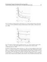
presented in Fig. 7. According to Fig. 7, our expectation that the the eigenfrequency level
ω corresponding to the extra vortex is situated inside the photonic band gap is true. We
calculated the frequency corresponding to the localized mode, which satisfies to the condition
of the validity of the dielectric contrast given by Eq. (15). According to Eqs. (20) and (21),
the localized field is decreasing proportionally to logξ
|r − r
0
|
−1
as the distance from an extra
vortex increases. Therefore, in order to detect this localized mode, the length of the film d
95
Electromagnetic Wave Propagation in Two-Dimensional Photonic Crystals
14 Electromagnetic Waves
Fig. 7. The dependence of the photonic band structure of the real Abrikosov lattice on B/B
c2
.
Solid line represents the eigenfrequency ω corresponding to the localized mode near the
extra vortex in the real Abrikosov lattice given by Eq. (18). The dashed and dotted lines
represent, respectively, the top ω
up
and bottom ω
dn
boundaries of the photonic band gap of
the ideal Abrikosov lattice according to Ref. (Takeda et al., 2004).
should not exceed approximately 10a
(B/B
c2
), which corresponds to d 200 μm for the range
of magnetic fields for the YBCO presented by Fig. 7. For these magnetic fields a
≈ 20 μm.
Since the frequency corresponding to the localized mode is situated inside the photonic
band gap, the extra vortex should be placed near the surface of the film as shown in Fig. 6.
Otherwise, the electromagnetic wave cannot reach this extra vortex. Besides, we assume that
this localized photonic state is situated outside the one-dimensional band of the surface states
of two-dimensional photonic crystal. It should be mentioned, that in a case of several extra
vortices separated at the distance greater than the size of one vortex (it is the coherence length
estimated for the YBCO by ξ
≈ 6.5 μm) the localized mode frequency for the both vortices is
also going to be determined by Eq. (18). The intensity of the localized mode in the latter case is
going to be enhanced due to the superposition of the modes localized by the different vortices.
In the case of far separated extra vortices we have neglected by the vortex-vortex interaction.
Thus, the existence of other pinned by crystal defects vortices increases the intensity of the
transmitted mode and improves the possibility of this signal detection. Note that at the
frequencies ω inside the photonic band gap ω
dn
< ω < ω
up
the transmittance and reflectance
of electromagnetic waves would be close to zero and one, correspondingly, everywhere except
the resonant frequency ω related to an extra vortex. The calculation of the transmittance
and reflectance of electromagnetic waves at this resonant frequency ω is a very interesting
problem, which will be analyzed elsewhere.
We considered a type-II superconducting medium with an extra Abricosov vortex pinned
by a defect in a superconductor. The discrete photonic eigenfrequency corresponding
to the localized photonic mode, is calculated as a function of the ratio B/B
c2
, which
parametrically depends on temperature. This photonic frequency increases as the ratio B/B
c2
and temperature T increase. Moreover, since the localized field and the corresponding
96
Wave Propagation
Electromagnetic Wave Propagation in Two-Dimensional Photonic Crystals 15
photonic eigenfrequency depend on the distance between the nearest Abrikosov vortices
a
(B,T), the resonant properties of the system can be tuned by control of the external magnetic
field B and temperature T. Based on the results of our calculations we can conclude that it
is possible to obtain a new type of a tunable far infrared monochromatic filter consisting of
extra vortices placed out of the nodes of the ideal Abrikosov lattice, which can be considered
as real photonic crystals. These extra vortices are pinned by a crystal defects in a type-II
superconductor in strong magnetic field. As a result of change of an external magnetic field B
and temperature T the resonant transmitted frequencies can be controlled.
5. Graphene-based photonic crystal
A novel type of 2D electron system was experimentally observed in graphene, which
is a 2D honeycomb lattice of the carbon atoms that form the basic planar structure in
graphite (Novoselov et al., 2004; Luk’yanchuk & Kopelevich, 2004; Zhang et al., 2005). Due to
unusual properties of the band structure, electronic properties of graphene became the object
of many recent experimental and theoretical studies (Novoselov et al., 2004; Luk’yanchuk &
Kopelevich, 2004; Zhang et al., 2005; Novoselov et al., 2005; Zhang et al., 2005; Kechezhdi et
al., 2008; Katsnelson, 2008; Castro Neto et al., 2009). Graphene is a gapless semiconductor
with massless electrons and holes which have been described as Dirac-fermions (Novoselov
et al., 2004; Luk’yanchuk & Kopelevich, 2004; Das Sarma et al., 2007). The unique electronic
properties of graphene in a magnetic field have been studied recently (Nomura & MacDonald,
2006; T
˝
oke et al., 2006; Gusynin & Sharapov, 2005;?). It was shown that in infrared and at
larger wavelengths transparency of graphene is defined by the fine structure constant (Nair
et al., 2008). Thus, graphene has unique optical properties. The space-time dispersion of
graphene conductivity was analyzed in Ref. (Falkovsky & Varlamov, 2007) and the optical
properties of graphene were studied in Refs. (Falkovsky & Pershoguba, 2007; Falkovsky,
2008).
In this Section, we consider a 2D photonic crystal formed by stacks of periodically placed
graphene discs embedded into the dielectric film proposed in Ref. (Berman et al., 2010). The
stack is formed by graphene discs placed one on top of another separated by the dielectric
placed between them as shown in Fig. 8. We calculate the photonic band structure and
transmittance of this graphene-based photonic crystal. We will show that the graphene-based
photonic crystals can be applied for the devices for the far infrared region of spectrum.
Let us consider polarized electromagnetic waves with the electric field E parallel to the
graphene discs. The wave equation for the electric field in a dielectric media has the
form (Landau & Lifshitz, 1984)
−E(r,t)+∇(∇·E(r, t)) −
ε(r)
c
2
∂
2
E(r,t)
∂t
2
= 0 , (23)
where ε
(r,t) is the dielectric constant of the media.
In photonic crystals, dielectric susceptibility is a periodical function and it can be expanded in
the Fourier series:
ε
(r)=
∑
G
ε(G)e
iGr
, (24)
where G is the reciprocal photonic lattice vector.
Expanding the electric field on the Bloch waves inside a photonic crystal, and seeking
solutions with harmonic time variation of the electric field, i.e., E
(r,t)=E(r)e
iωt
, one obtains
97
Electromagnetic Wave Propagation in Two-Dimensional Photonic Crystals
16 Electromagnetic Waves
k
&
E
&
b)
Graphene discs Dielectric discs Dielectric substrate
k
&
a)
Fig. 8. Graphene-based photonic crystal: a) the side view. The material of the dielectric
between graphene discs can be the same as the material of the dielectric substrate; b) the top
view.
from Eq. (23) using Eq. (24) the system of equations for Fourier components of the electric
field (Joannopoulos et al., 2008; McGurn & Maradudin, 1993):
(k + G)
2
E
k
(G)=
ω
2
(k)
c
2
∑
G
ε(G −G
)E
k
(G
) , (25)
which presents the eigenvalue problem for finding photon dispersion curves ω
(k). In Eq. (25)
the coefficients of the Fourier expansion for the dielectric constant are given by
ε
(G −G
)=ε
0
δ
GG
+(ε
1
−ε
0
)M
GG
. (26)
In Eq. (26) ε
0
is the dielectric constant of the dielectric, ε
1
is the dielectric constant of graphene
multilayers separated by the dielectric material, and M
GG
for the geometry considered above
is
M
GG
= 2 f
J
1
(|G −G
|r)
(|G −G
|r)
, G = G
,
M
GG
= f , G = G
, (27)
where J
1
is the Bessel function of the first order, and f = S
g
/S is the filling factor of 2D
photonic crystal.
In our consideration the size of the graphene discs was assumed to be much larger than the
period of the graphene lattice, and we applied the expressions for the dielectric constant of
the infinite graphene layer for the graphene discs, neglecting the effects related to their finite
size.
The dielectric constant ε
1
(ω) of graphene multilayers system separated by the dielectric layers
with the dielectric constant ε
0
and the thickness d is given by (Falkovsky & Pershoguba, 2007;
98
Wave Propagation
Electromagnetic Wave Propagation in Two-Dimensional Photonic Crystals 17
Falkovsky, 2008)
ε
1
(ω)=ε
0
+
4πiσ
g
(ω)
ωd
, (28)
where σ
g
(ω) is the dynamical conductivity of the doped graphene for the high frequencies
(ω
kv
F
, ω τ
−1
) at temperature T given by (Falkovsky & Pershoguba, 2007; Falkovsky,
2008)
σ
g
(ω)=
e
2
4¯h
[
η(¯hω −2μ)
+
i
2π
16k
B
T
¯hω
log
2cosh
μ
2k
B
T
−log
(¯hω + 2μ)
2
(¯hω −2μ)
2
+(2k
B
T)
2
. (29)
Here τ
−1
is the electron collision rate, k is the wavevector, v
F
= 10
8
cm/s is the Fermi velocity
of electrons in graphene (Falkovsky, 2008), and μ is the the chemical potential determined
by the electron concentration n
0
=(μ/(¯hv
F
))
2
/π, which is controlled by the doping. The
chemical potential can be calculated as μ
=(πn
0
)
1/2
¯hv
F
. In the calculations below we assume
n
0
= 10
11
cm
−2
. For simplicity, we assume that the dielectric material is the same for the
dielectric discs between the graphene disks and between the stacks. As the dielectric material
we consider SiO
2
with the dielectric constant ε
0
= 4.5.
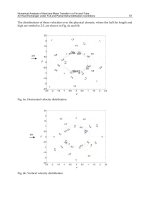
To illustrate the effect let us, for example, consider the 2D square lattice formed by the
graphene based metamaterial embedded in the dielectric. The photonic band structure for
the graphene based 2D photonic crystal with the array of cylinders arranged in a square
lattice with the filling factor f
= 0.3927 is presented in Fig. 9. The cylinders consist of the
metamaterial stacks of alternating graphene and dielectric discs. The period of photonic
crystal is a
= 25 μm, the diameter of discs is D = 12.5 μm, the width of the dielectric layers
d
= 10
−3
μm . Thus the lattice frequency is ω
a
= 2πc/a = 7.54 × 10
13
rad/s. The results
of the plane wave calculation for the graphene based photonic crystal are shown in Fig. 9,
and the transmittance spectrum obtained using the Finite-Difference Time-Domain (FDTD)
method (Taflove, 1995) is presented in Fig. 10. Let us mention that plane wave computation
has been made for extended photonic crystal, and FDTD calculation of the transmittance have
been performed for five graphene layers. A band gap is clearly apparent in the frequency
range 0
< ω < 0.6 and 0.75 < ω < 0.95 in units of 2πc/a. The first gap is originated from
the electronic structure of the doped graphene, which prevents absorbtion at ¯hω
< 2μ (see
also Eq. (29)). The photonic crystal structure manifests itself in the dependence of the lower
photonic band on the wave vector k. In contrast, the second gap 0.75
< ω < 0.95 is caused by
the photonic crystal structure and dielectric contrast.
According to Fig. 10, the transmittance T is almost zero for the frequency lower than 0.6ω
a
,
which corresponds to the first band gap shown in Fig. 9. The second gap in Fig. 9 (at the
point G) corresponds to ω
= 0.89ω
a
, and it also corresponds to the transmittance spectrum
minimum on Fig. 10.
Let us mention that at ¯hω
< 2μ the dissipation of the electromagnetic wave in graphene is
suppressed. In the long wavelength (low frequency) limit, the skin penetration depth is given
by δ
0
(ω)=c/Re
2πωσ
g
(ω)
1/2
(Landau & Lifshitz, 1984). According to Eq. (29), Re[σ
g
(ω <
2μ)] = 0, therefore, δ
0
(ω) →+∞, and the electromagnetic wave penetrates along the graphene
99
Electromagnetic Wave Propagation in Two-Dimensional Photonic Crystals
18 Electromagnetic Waves
G
M
X
b)
Fig. 9. a) Band structure of graphene based 2D square photonic crystal of cylinder array
arranged in a square lattice. The cylinders consist of stack of graphene monolayer discs
separated by the dielectric discs. The filling factor f
= 0.3927. M, G, X, M are points of
symmetry in the first (square) Brillouin zone. b) The first Brillouin zone of the 2D photonic
crystal.
layer without damping. For the carrier densities n
0
= 10
11
cm
−2
the chemical potential is
μ
= 0.022 eV (Falkovsky & Pershoguba, 2007), and for the frequencies ν < ν
0
= 10.42 THz
we have Re
[σ
g
(ω)] = 0atω 1/τ the electromagnetic wave penetrates along the graphene
Fig. 10. The transmittance T spectrum of graphene based 2D photonic crystal.
100
Wave Propagation
Electromagnetic Wave Propagation in Two-Dimensional Photonic Crystals 19
layer almost without damping, which makes the graphene multilayer based photonic crystal
to be distinguished from the metallic photonic crystal, where the electromagnetic wave is
essentially damped. As a result, the graphene-based photonic crystals can have the sizes much
larger than the metallic photonic crystals. The scattering of the electrons on the impurities can
result in non-zero Re
[σ
g
(ω)], which can cause the dissipation of the electromagnetic wave.
Since the electron mobility in graphene can be much higher than in typical semiconductors,
one can expect that the scattering of the electrons on the impurities does not change the results
significantly.
The physical properties of graphene-based photonic crystals are different from the physical
properties of other types of photonic crystals, since the dielectric constant of graphene has the
unique frequency dependence (Falkovsky & Pershoguba, 2007; Falkovsky, 2008). According
to the results presented above, the graphene-based photonic crystal has completely different
photonic band structure in comparison to the photonic crystals based on the other materials.
The photonic band structure of the photonic crystal with graphene multilayer can be tuned
by changing the distance d between graphene discs in the r.h.s. of Eq. (28). The photonic
band structure of the graphene-based photonic crystals can also be controlled by the doping,
which determines the chemical potential μ entering the expressions for the conductivity and
dielectric constant of graphene multilayer (29).
6. Discussion and conclusions
Comparing the photonic band structure for graphene-based photonic crystal presented
in Fig. 9 with the dielectric (Joannopoulos et al., 2008), metallic (McGurn & Maradudin,
1993; Kuzmiak & Maradudin, 1997), semiconductor (McGurn & Maradudin, 1993) and
superconductor-based (Berman et al., 2006; Lozovik et al., 2007) photonic crystals, we
conclude that only graphene- and superconductor-based photonic crystals have essential
photonic band gap at low frequencies starting ω
= 0, and the manifestation of the gap
in the transmittance spectra is almost not suppressed by the damping effects. Therefore,
only graphene-based and superconducting photonic crystals can be used effectively as the
frequency filters and waveguides in low-frequency for the far infrared region of spectrum,
while the devices based on the dielectric photonic crystals can be used only in the optical
region of electromagnetic waves spectrum. The graphene based-photonic crystal can be used
at room temperatures, while the superconductor-based photonic crystal can be used only
at low temperatures below the critical temperature T
c
, which is about 90 K for the YBCO
superconductors.
In summary, photonic crystals are artificial media with a spatially periodical dielectric function.
Photonic crystals can be used, for example, as the optical filters and waveguides. The
dielectric- and metal-based photonic crystals have different photonic bands and transmittance
spectrum. It was shown that the photonic band structure of superconducting photonic crystal
leads to their applications as optical filters for far infrared frequencies . It is known that the
dielectric- and metal-based photonnic crystals with defects can be used as the waveguides
for the frequencies corresponding to the media forming the photonic crystals. Far infrared
monochromatic transmission across a lattice of Abrikosov vortices with defects in a type-II
superconducting film is predicted. The transmitted frequency corresponds to the photonic
mode localized by the defects of the Abrokosov lattice. These defects are formed by extra
vortices placed out of the nodes of the ideal Abrokosov lattice. The extra vortices can
be pinned by crystal lattice defects of a superconductor. The corresponding frequency is
studied as a function of magnetic field and temperature. The control of the transmitted
101
Electromagnetic Wave Propagation in Two-Dimensional Photonic Crystals
20 Electromagnetic Waves
frequency by varying magnetic field and/or temperature is analyzed. It is suggested that
found transmitted localized mode can be utilized in the far infrared monochromatic filters.
Besides, infrared monochromatic transmission through a superconducting multiple conductor
system consisting of parallel superconducting cylinders is found. The transmitted frequency
corresponds to the localized photonic mode in the forbidden photonic band, when one
superconducting cylinder is removed from the node of the ideal two-dimensional lattice of
superconducting cylinders. A novel type of photonic crystal formed by embedding a periodic
array of constituent stacks of alternating graphene and dielectric discs into a background
dielectric medium is proposed. The frequency band structure of a 2D photonic crystal with
the square lattice of the metamaterial stacks of the alternating graphene and dielectric discs
is obtained. The electromagnetic wave transmittance of such photonic crystal is calculated.
The graphene-based photonic crystals have the following advantages that distinguish them
from the other types of photonic crystals. They can be used as the frequency filters for the
far-infrared region of spectrum at the wide range of the temperatures including the room
temperatures. The photonic band structure of the graphene-based photonic crystals can be
controlled by changing the thickness of the dielectric layers between the graphene discs and
by the doping. The sizes of the graphene-based photonic crystals can be much larger than the
sizes of metallic photonic crystals due to the small dissipation of the electromagnetic wave.
The graphene-based photonic crystals can be used effectively as the frequency filters and
waveguides for the far infrared region of electromagnetic spectrum. Let us also mention that
above for simplicity we assume that the dielectric material is the same between the graphene
disks and between the stacks. This assumption has some technological advantage for the most
easier possible experimental realization of the graphene-based photonic crystal.
7. References
Abrikosov, A. A. (1988). Fundamentals of the Theory of Metals (North Holland, Amsterdam).
Berman, O. L., Boyko, V. S., Kezerashvili, R. Ya., and Lozovik, Yu .E. (2008). Anomalous
far-infrared monochromatic transmission through a film of type-II superconductor
in magnetic field. Phys. Rev. B, 78, 094506.
Berman, O. L., Boyko, V. S., Kezerashvili, R. Ya., and Lozovik, Yu .E. (2009). Monochromatic
Infrared Wave Propagation in 2D Superconductor
−Dielectric Photonic Crystal. Laser
Physics, 19, No. 10, pp. 2035
−2040.
Berman, O. L., Boyko, V. S., Kezerashvili, R. Ya., Kolesnikov, A. A., and Lozovik, Yu .E. (2010).
Graphene-based photonic crystal. Physics Letters A, 374, pp. 4784
−4786.
Berman, O. L., Lozovik, Yu. E., Eiderman, S. L., and Coalson, R. D. (2006). Superconducting
photonic crystals: Numerical calculations of the band structure. Phys. Rev. B, 74,
092505.
Castro Neto, A. H., Guinea, F.,, Peres, N. M. R., Novoselov, K. S. and Geim, A. K. (2009). The
electronic properties of graphene, Reviews of Modern Physics, 81, pp. 109–162.
Chigrin, D. N. and Sotomayor Torres, C. M (2003). Self-guiding in two-dimensional photonic
crystals. Optics Express, 11, No 10, pp. 1203–1211.
Das Sarma, S., Hwang, E. H., and Tse, W. K. (2007). Many-body interaction effects in doped
and undoped graphene: Fermi liquid versus non-Fermi liquid. Phys. Rev. B, 75,
121406(R).
Falkovsky, L. A. and Pershoguba, S. S. (2007). Optical far-infrared properties of a graphene
monolayer and multilayer. Phys. Rev. B, 76, 153410.
Falkovsky, L. A. and Varlamov, A A. (2007). Space-time dispersion of graphene conductivity.
102
Wave Propagation
Electromagnetic Wave Propagation in Two-Dimensional Photonic Crystals 21
Eur. Phys. J. B 56, pp. 281–284.
Falkovsky, L. A. (2008). Optical properties of graphene. J. Phys.: Conf. Ser., 129, 012004.
Gusynin, V. P. and Sharapov, S. G. (2005). Magnetic oscillations in planar systems with the
Dirac-like spectrum of quasiparticle excitations. II. Transport properties, Phys. Rev.
B, 71, 125124.
Gusynin, V. P. and Sharapov, S. G. (2005). Unconventional Integer Quantum Hall Effect in
Graphene, Phys. Rev. Lett., 95, 146801.
Joannopoulos, J. D., Meade, R. D., and Winn, J. N. (1995). Photonic Crystals: The Road from
Theory to Practice (Princeton University Press, Princeton, NJ).
Joannopoulos, J. D., Johnson, S. G., Winn, J. N., and Meade, R. D. (2008). Photonic Crystals:
Molding the Flow of Light (Second Edition, Princeton University Press, Princeton, NJ).
John, S. (1987). Strong localization of photons in certain disordered dielectric superlattices.
Phys. Rev. Lett., 58, pp. 2486–2489.
Katsnelson, M. I. (2008). Optical properties of graphene: The Fermi liquid approach.
Europhys. Lett., 84, 37001.
Kechedzhi, K., Kashuba O., and Fal’ko, V. I. (2008). Quantum kinetic equation and universal
conductance fluctuations in graphene. Phys. Rev. B, 77, 193403.
Keldysh, L. V. (1964). Deep levels in semiconductors. Sov. Phys. JETP 18, 253.
Kohn, W. (1957). In Solid State Physics, edited by F. Seitz and D. Turnbull, vol. 5, pp. 257–320
(Academic, New York).
Kuzmiak, V. and Maradudin, A. A. (1997). Photonic band structures of one- and
two-dimensional periodic systems with metallic components in the presence of
dissipation. Phys. Rev. B 55, pp. 7427–7444.
Landau. L. D. and Lifshitz, E. M. (1984). Electrodynamics of continuous media. (Second Edition,
Pergamon Press, Oxford).
Lozovik, Yu. E., Eiderman, S. I., and Willander, M. (2007). The two-dimensional
superconducting photonic crystal. Laser physics, 9, No 17, pp. 1183–1186.
Luk’yanchuk, I. A. and Kopelevich, Y. (2004). Phase Analysis of Quantum Oscillations in
Graphite. Phys. Rev. Lett., 93, 166402.
Luttinger, J. M. and Kohn, W. (1955). Motion of Electrons and Holes in Perturbed Periodic
Fields. Phys. Rev., 97, pp. 869–883.
McGurn, A. R. and Maradudin, A. A. (1993). Photonic band structures of two- and
three-dimensional periodic metal or semiconductor arrays. Phys. Rev. B, 48, pp.
17576–17579.
Meade, R. D., Brommer, K. D., Rappe, A. M., and Joannopoulos, J. D. (1991). Photonic bound
states in periodic dielectric materials. Phys. Rev. B, 44, pp. 13772–13774.
Meade, R. D., Brommer, K. D., Rappe, A. M. and Joannopoulos, J. D. (1992). Existence of a
photonic band gap in two dimensions. Appl. Phys. Lett., 61, pp. 495–497.
Meade, R. D., Rappe, A. M., Brommer K. D., Joannopoulos, J. D., and Alerhand, O. L. (1993).
Accurate theoretical analysis of photonic band-gap materials. Phys. Rev. B 48, pp.
8434–8437.
McCall, S. L., Platzmann, P. M., Dalichaouch R., Smith, D. and Schultz, S. (1991). Microwave
propagation in two-dimensional dielectric lattices. Phys. Rev. Lett. 67, pp. 2017–2020.
Nair, R. R., Blake, P., Grigorenko, A. N., Novoselov, K. S., Booth, T. J., Stauber, T.,
Peres, N. M. R., and Geim, A. K. (2008). Fine Structure Constant Defines Visual
Transparency of Graphene. Science, 320, no. 5881, 1308.
Nomura, K. and MacDonald, A. H. (2006). Quantum Hall Ferromagnetism in Graphene.
103
Electromagnetic Wave Propagation in Two-Dimensional Photonic Crystals
22 Electromagnetic Waves
Phys. Rev. Lett., 96, 256602.
Novoselov, K. S., Geim, A. K., Morozov, S. V., Jiang, D., Zhang, Y., Dubonos, S. V., Grigorieva,
I. V., and Firsov, A. A. (2004). Electric Field Effect in Atomically Thin Carbon Films.
Science, 306, no. 5696, pp. 666–669.
Novoselov, K. S., Geim, A. K., Morozov, S. V., Jiang, D., Katsnelson, M. I., Grigorieva, I. V.
and Dubonos, S. V., (2005). Two-Dimensional Gas of Massless Dirac Fermions in
Graphene. Nature (London), 438, pp. 197–200.
Robertson, W. M., Arjavalingam, G., Meade, R. D., Brommer, K. D., Rappe, A. M.,
and Joannopoulos, J. D. (1992). Measurement of photonic band structure in a
two-dimensional periodic dielectric array, Phys. Rev. Lett., 68, pp. 2023–2026.
Safar, H., Gammel, P. L., Huse, D. A., Majumdar, S. N., Schneemeyer, L. F., Bishop, D. J.,
L
´
opez, D., Nieva, G., and de la Cruz, F. (1994). Observation of a nonlocal conductivity
in the mixed state of YBa
2
Cu
3
O
7−δ
: Experimental evidence for a vortex line liquid.
Phys. Rev. Lett., 72, pp. 1272–1275.
Taflove, A. (1995). Computational Electrodynamics: The Finite-Difference Time-Domain Method
(MA: Artech House).
Takeda, H. and Yoshino, K. (2003). Tunable light propagation in Y-shaped waveguides
in two-dimensional photonic crystals utilizing liquid crystals as linear defects.
Phys. Rev. B, 67, 073106.
Takeda, H. and Yoshino, K. (2003). Tunable photonic band schemes in two-dimensional
photonic crystals composed of copper oxide high-temperature superconductors.
Phys. Rev. B, 67, 245109.
Takeda, H., Yoshino, K., and Zakhidov, A. A. (2004). Properties of Abrikosov lattices as
photonic crystals. Phys. Rev. B, 70, 085109.
Takhtamirov, E. E. and Volkov, V. A. (1999). Generalization of the effective mass method for
semiconductor structures with atomically sharp heterojunctions. JETP, 89, No 5, pp.
1000–1014.
T
˝
oke, C., Lammert, P. E., Crespi, V. H., and Jain, J. K. (2006). Fractional quantum Hall effect in
graphene. Phys. Rev. B, 74, 235417.
Yablonovitch, E. (1987). Inhibited Spontaneous Emission in Solid-State Physics and
Electronics, Phys. Rev. Lett., 58, pp. 2059–2062.
Yablonovitch, E., Gmitter, T. J., Meade, R. D., Brommer, K. D., Rappe, A. M., and Joannopoulos,
J. D. (1991). Donor and acceptor modes in photonic band structure. Phys. Rev. Lett.,
67, pp. 3380–3383.
Zhang, Y., Small, J. P., Amori, M. E. S., and Kim P. (2005). Electric Field Modulation of
Galvanomagnetic Properties of Mesoscopic Graphite. Phys. Rev. Lett., 94, 176803.
Zhang, Y., Tan, Y W., Stormer, H. L., and Kim, P. (2005). Experimental observation of the
quantum Hall effect and Berry’s phase in graphene. Nature, 438, pp. 201–204.
104
Wave Propagation
6
Terahertz Electromagnetic Waves from
Semiconductor Epitaxial Layer Structures:
Small Energy Phenomena with a
Large Amount of Information
Hideo Takeuchi
Department of Electronic Systems Engineering, School of Engineering,
The University of Shiga Prefecture
Japan
1. Introduction
Terahertz electromagnetic waves have a frequency range between infrared light and
microwaves: the frequency of 1 THz corresponds to the photon energy of 4.1 meV (33 cm
-1
)
and to the wavelength of 300 μm. It is well known that the terahertz waves have a high
sensitivity to the water concentration in materials. For example, Hu and Nuss compared the
terahertz-wave transmittance image of the freshly cut leaf with that of the same leaf after 48
hours (Hu & Nuss, 1995). They demonstrated the freshness between the two leaves can be
clearly evaluated from the terahertz-wave transmittance images. In addition, the terahertz
waves are sensitive to explosive chemical materials (Yamamoto et al., 2004). Accordingly,
the terahertz waves are applicable to a security system in airports because conventional x-
ray inspection systems are insensitive to chemical materials. The above-mentioned
characteristics of the terahertz wave lead to the reason why terahertz-wave spectroscopy is
attractive. We note that the terahertz waves are useful to investigate the vibration of
biological molecules, dielectric constant of materials, and so on (Nishizawa et al., 2005).
In the present chapter, we focus our attention on the time-domain terahertz-wave
measurements based on the femtosecond-pulse-laser technology. Most of the terahertz-
wave measurement systems employ photoconductive antenna devices (Auston, 1975; Nuss
& Orenstein, 1999) as an emitter of terahertz waves. As mentioned later, the antenna-based
terahertz emitters, which are categorized into a lateral/planer structure type emitter, have
various disadvantages. For the progress in terahertz-wave spectroscopy, it is still required to
develop convenient terahertz-wave emitters. Compound semiconductors with a surface
electric field, by being irradiated by femtosecond-laser pulses, emit the terahertz wave
originating from the surge current of the photogenerated carriers flowing from the surface
to the internal side in the surface depletion layer. This phenomenon provides us a
convenient terahertz emitter free from a device fabrication for an external applied bias. In
the above terahertz emission mechanism, the doping concentration is a major factor
determining the depletion-layer width and surface electric field, which are in the relation of
trade-off. In order to obtain intense terahertz wave emission, earlier works focused on