Wave Propagation 2010 Part 6 doc
Bạn đang xem bản rút gọn của tài liệu. Xem và tải ngay bản đầy đủ của tài liệu tại đây (620.42 KB, 30 trang )
Wave Propagation
142
8. Result/discussion
0
0.2
0.4
0.6
0.8
1
1.2
1.4
0.00 1.00 2.00 3.00 4.00 5.00 6.00
Propagation Distance (x10E-06m)
Field
0.90x10E-06m
0.70x10E-06m
0.4x10E-06m
Fig. 1. The field behaviour as it propagates through the film thickness Zμm for mesh size =
10 when λ =0.4μm 0.7μm and 0.9μm.
0.00
0.20
0.40
0.60
0.80
1.00
1.20
0.00 1.00 2.00 3.00 4.00 5.00 6.00
Propagation Distance (x10E-06m)
Field
0.9x10E-06m
0.70x10E-06m
0.25x10E-06m
Fig. 2. The field behaviour as it propagates through the film thickness Zμm for mesh size =
50 when λ = 0.25μm, 0.7μm and 0.9μm.
Wave Propagation in Dielectric Medium Thin Film Medium
143
-0.6
-0.4
-0.2
0
0.2
0.4
0.6
0.8
1
1.2
1.4
0.0000 1.0000 2.0000 3.0000 4.0000 5.0000 6.0000
Propagation Distance (x10E-06m)
Field
1.20x10E-06m
0.70x10E-06m
0.35x10E-06m
Fig. 3. The field behavour as it propagates through the film thickness Zμm for mesh size =
50 when λ = 0.25μm, 0.7μm and 0.9μm.
-1
-0.5
0
0. 5
1
1. 5
0. 00 1. 00 2. 00 3. 00 4.0 0 5.00 6. 00
Pr opagat i on Dist ance ( x10 E - 0 6 m)
1. 35x10E-06m
0. 8x10E-06m
0. 25x10E-06m
Fig. 4. The field behavour as it propagates through the film thickness Zμm for mesh size =
100 when λ = 0.25μm, 0.8μm and 1.35μm.
Wave Propagation
144
0
0. 1
0. 2
0. 3
0. 4
0. 5
0. 6
0. 7
0 0. 2 0. 4 0.6 0. 8 1 1. 2 1.4
mm
T
a
b
Se r i es1
Ψab
λμm
Fig. 5. The filed absorbance as a function wavelength.
nz()
z
10 7.5 5 2.5 0 2.5 5 7.5 10
2.18
2.185
2.19
2.195
2.2
2.205
2.21
2.215
2.22
2.225
2.23
Fig. 6. Refractive index profile using Fermi distribution
Wave Propagation in Dielectric Medium Thin Film Medium
145
Δnz()
z
1 10
0
0.0016
0.0032
0.0048
0.0064
0.008
Propagation distance
Change in Refractive index
Fig. 7. Graph of change in Refractive Index as a function of a propagation distance
Rn()
n
1 10
2
4
6
8
10
Im pedance
Fig. 8. Graph of Impedance against Refractive Index when k =k
0
Wave Propagation
146
0
50
100
150
200
250
300
350
400
0 0.2 0.4 0.6 0.8 1 1.2
Wavelegth
Computed Field
Fig. 9. Computed field against wavelength when the mesh size is constant
0.0000
2.0000
4.0000
6.0000
8.0000
10.0000
12.0000
14.0000
0.0000 0.0200 0.0400 0.0600 0.0800 0.1000 0.1200
Green's Value
Computed Field Value
Initial Field Value
Fig. 10. Computed and Initial field values in relation to the Green’s value within the uv
region
Wave Propagation in Dielectric Medium Thin Film Medium
147
0.0000
2.0000
4.0000
6.0000
8.0000
10.0000
12.0000
14.0000
0.0000 0.0200 0.0400 0.0600 0.0800 0.1000 0.1200
Green's Value
Computed Field Value / 20
Initial Field Value
Fig. 11. Computed and Initial field values in relation to the Green’s value within the near
infrared region
0.0000
2.0000
4.0000
6.0000
8.0000
10.0000
12.0000
14.0000
0.0000 0.0200 0.0400 0.0600 0.0800 0.1000 0.1200
Green's Value
Computed Field Value / 20
Initial Field Value
Fig. 12. Computed and Initial field values in relation to the Green’s value within the visible
region
Wave Propagation
148
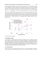
From the result obtained using this formalism, the field behaviour over a finite distance was
contained and analyzed by applying born approximation method in Lippman-Schwinger
equation involving step by step process. The result yielded reasonable values in relation to
the experimental result of the absorption behaviour of the thin film (Ugwu, 2001).
The splitting of the thickness into more finite size had not much affected on the behaviour of
the field as regarded the absorption trends.
The trend of the graph obtained from the result indicated that the field behaviour have the
same pattern for all mesh size used in the computation. Though, there is slight fall in
absorption within the optical region, the trend of the graph look alike when the thickness is
1.0
μ
m with minimum absorption occurring when the thickness is 0.5
μ
m. within the near
infrared range and ultraviolet range, (0.25
μ
m) the absorption rose sharply, reaching a
maximum of1.48 and 1.42 respectively when thickness is 1.0
μ
m having value greater than
unity.
From the behaviour of the propagated field for the specified region, UV, Visible and Near
infrared, (Ugwu, 2001) the propagation characteristic within the optical and near infrared
regions was lower when compared to UV region counterpart irrespective of the mesh size
and the number of points the thickness is divided. The field behaviour was unique within
the thin film as observed in fig. 3 and fig 4: for wavelength 1.2μm and 1.35μm
while that of fig,1 and fig.2 were different as the wave patterns were shown within the
positive portion of the graph. The field unique behavior within the film medium as
observed in the graphs in fig.1 to fig.4 for all the wave length and N
max
suggests the
influence of scattering and reflection of the propagated field produced by the particles of the
thin field medium. The peak as seen in the graphs is as a result of the first encounter of the
individual molecules of the thin film with the incident radiation. The radiation experiences
scattering by the individual molecules at first conforming to Born and Huang, 1954 where it
was explained that when a molecule initially in a normal state is excited, it generates
spontaneous radiation of a given frequency that goes on to enhance the incident radiation
This is because small part of the scattered incident radiation combines with the primary
incident wave resulting in phase change that is tantamount to alternation of the wave
velocity in the thin film medium. One expects this peat to be maintained, but it stabilized as
the propagation continued due to fact that non-forward scattered radiation is lost from the
transmitted wave(Sanders,19980) since the thin film medium is considered to be optically
homogeneous, non-forward scattered wave is lost on the account of destructive interference.
In contrast, the radiation scattered into the forward direction from any point in the medium
interferes constructively (Fabelinskii, 1968)
We also observed in each case that the initial value of the propagation distance zμm, initial
valve of the propagating field is low, but increase sharply as the propagation distance
increases within the medium suggesting the influence of scattering and reflection of
propagating field produced by the particles of the thin film as it propagates.Again, as high
absorption is observed within the ultraviolet (UV) range as depicted in fig.5, the thin film
could be used as UV filter on any system the film is coated with as it showed high
absorption. On other hand, it was seen that the absorption within the optical (VIS) and near
infrared (NIR) regions of solar radiation was low. Fig.6 depicts the refractive index profile
according to equation (41) while that of the change in refractive index with propagation
distant is shown on figs.7. The impedance appears to have a peak at lower refractive index
as shown in fig. 8. Fig. 9 shows the field profile for a constant mesh size while that of Fig.10
Wave Propagation in Dielectric Medium Thin Film Medium
149
to fig.12 are profile for the three considered regions of electromagnetic radiation as obtained
from the numerical consideration.
9. Conclusion
A theoretical approach to the computation and analysis of the optical properties of thin film
were presented using beam propagation method where Green’s function, Lippmann-
Schwinger and Dyson’s equations were used to solve scalar wave equation that was
considered to be incident to the thin film medium with three considerations of the thin film
behaviour These includes within the three regions of the electromagnetic radiation namely:
ultra violet, visible and infrared regions of the electromagnetic radiation with a
consideration of the impedance offered to the propagation of the field by the thin film
medium.
Also, a situation where the thin film had a small variation of refractive index profile that
was to have effect on behaviour of the propagated field was analyzed with the small
variation in the refractive index. The refractive index was presented as a small perturbation.
This problem was solved using series solution on Green’s function by considering some
boundary conditions (Ugwu et al 2007). Fermi distribution function was used to illustrate
the refractive index profile variation from where one drew a close relation that facilitated an
expression that led to the analysis of the impedance of the thin film
The computational technique facilitated the solution of field values associated first with the
reference medium using the appropriate boundary conditions on Lippmann-Schwinger
equation on which dyadic Green’s operator was introduced and born approximation
method was applied both Lippmann-Schwinger and Dyson’s equations. These led to the
analysis of the propagated field profile through the thin film medium step by step.
10. Reference
[1] A.B Cody, G. Brook and Abele 1982 “Optical Absorption above the Optical Gap of
Amorphous Silicon Hydride”. Solar Energy material, 231-240.
[2] A.D Yaghjian 1980 “Electric dynamic green’s functions in the source region’s Proc IEEE
68,248-263.
[3] Abeles F. 1950 “Investigations on Propagation of Sinusoidal Electromagnetic Waves in
Stratified Media Application to Thin Films”, Ann Phy (Paris) 5 596- 640.
[4] Born M and Huang K 1954, Dynamical theory of crystal lattice Oxford Clarendon
[5] Born, M and Wolf E, 1980, “Principle of optics” 6
th
Ed, Pergamon N Y.
[6] Brykhovestskii, A.S, Tigrov,M and I.M Fuks 1985 “Effective Impendence Tension Of
Computing Exactly the Total Field Propagating in Dielectric Structure of arbitrary
shape”. J. opt soc Am A vol 11, No3 1073-1080.
[7] E.I. Ugwu 2005 “Effects of the electrical conductivity of thin film on electromagnetic
wave propagation. JICCOTECH Maiden Edition. 121-127.
[8] E.I. Ugwu, C.E Okeke and S.I Okeke 2001.”Study of the UV/optical properties of FeS
2
thin film Deposited by solution Growth techniques JEAS Vol1 No. 13-20.
[9] E.I. Ugwu, P.C Uduh and G.A Agbo 2007 “The effect of change in refractive index on
wave propagation through (feS
2
) thin film”. Journal of Applied Sc.7 (4). 570-574.
[10] E.N Economou 1979 “Green’s functions in Quantum physics”, 1
st
. Ed. Springer. Verlag,
Berlin.
Wave Propagation
150
[11] F.J Blatt 1968 “Physics of Electronic conduction in solid”. Mc Graw – Hill Book Co Ltd
New York, 335-350.
[12] Fablinskii I. L, 1968 Molecular scattering of light New York Plenum Press.
[13] Fitzpatrick, .R, (2002), “Electromagnetic wave propagation in dielectrics”. http: //
farside. Ph. U
Texas. Edu/teaching/jkl/lectures/node 79 htmil. Pp 130 – 138.
[14] G. Gao, C Tores – Verdin and T.M Hat 2005 “Analytical Techniques toe valuate the
integration of 3D and 2D spatial Dyadic Green’s function” progress in
Electromagnetic Research PIER 52, 47-80.
[15] G.W. Hanson 1996 “A Numerical formation of Dyadic Green’s functions for planar
Bianisotropic Media with Application to printed Transmission line” IEEE
Transaction on Microwave theory and techniques, 44(1).
[16] H.L Ong 1993 “2x2 propagation matrix for electromagnetic waves propagating
obliquely in layered inhomogeneous unaxial media” J.Optical Science A/10(2). 283-
393.
[17] Hanson, G W, (1996), “A numerical formulation of Dyadic Green’s functions for Planar
Bianisotropic Media with Application to Printed Transmission lines”. S 0018 – 9480
(96) 00469-3 lEEE pp144 – 151.
[18] J.A Fleck, J.R Morris and M.D. Feit 1976 “Time – dependent propagation of high energy
laser beans through the atmosphere” Applied phys 10,129-160.
[19] L. Thylen and C.M Lee 1992 “Beam propagation method based on matrix digitalization”
J. optical science A/9 (1). 142-146.
[20] Lee, J.K and Kong J.A 1983 Dyadic Green’s Functions for layered an isotropic medium.
Electromagn. Vol 3 pp 111-130.
[21] M.D Feit and J.A Fleck 1978 “Light propagation in graded – index optical fibers” Applied
optical17, 3990-3998.
[22] Martin J F Oliver, Alain Dereux and Christian Girard 1994 “Alternative Scheme of
[23] P.A. Cox 1978 “The electroni c structure and Chemistry of solids “Oxford University
Press Ch. 1-3. Plenum Press ; New York Press.
[24] Sanders P.G.H,1980 Fundamental Interaction and Structure of matters:
1
st
edition
[25] Smith E.G. and Thomos J.H., 1982. “Optics ELBS and John Wiley and Sons Ltd London.
Statically Rough Ideally Conductive Surface. Radioplys. Quantum Electro 703 -708
8
The Electrodynamic Properties of Structures
with Thin Superconducting Film in Mixed State
Mariya Golovkina
Povolzhskiy State University of Telecommunacations and Informatics
Russia
1. Introduction
Thin superconducting films are used in many areas of microwave technics. The discovery of
high temperature superconductors in 1986 (Bednorz & Muller, 1986) was a powerful
incentive to application of superconductors in science and engineering. High-temperature
superconductors have a lot of necessary microwave properties, for example: low insertion
loss, wide frequency band, low noise, high sensibility, low power loss and high reliability.
High-temperature superconductors have significant potential for applications in various
devices in microelectronics because of the ability to carry large amount of current by high
temperature (Zhao et al., 2002). The widely applicable high-temperature superconductor
YBa
2
Cu
3
O
7
with critical temperature T
c
=90 K keeps the superconductivity above the boiling
point of nitrogen. One of the applications of high-temperature superconductors is the
passive microwave device because of it extremely small resistance and low insertion loss. In
recent years new techniques have been developed for production of superconducting
layered systems. The superconducting films are indispensable for manufacture of resonators
and filters with the technical parameters that significantly surpass the traditional materials.
The progress in microsystem technologies and nanotechnologies enables the fabrication of
thin superconducting films with thickness about several atomic layers (Koster et al., 2008),
(Chiang, 2004). Due to new technologies scientists produce a thin film which exhibits a
nanometer-thick region of superconductivity (Gozar et al., 2008).
The thin superconducting films are more attractive for scientists and engineers than the bulk
superconducting ceramics. The thin films allow to solve a problem of heat think. The
application of thin films increases with the growth of critical current density J
c
. Nowadays it
is known a large number of superconducting materials with critical temperature above 77 K.
But despite of the bundle of different high-temperature superconducting compounds, only
three of group have been widely used in thin film form: YBa
2
Cu
3
O
7
, Bi
v
Sr
w
Ca
x
Cu
y
O
z
,
Tl
v
Ba
w
Ca
x
Cu
y
O
z
(Phillips, 1995). YBa
2
Cu
3
O
7
has critical temperature T
c
=90 K (Wu et al.,
1987) and critical current density J
c
=5⋅10
10
A/m
2
at 77 K (Yang et al., 1991), (Schauer et al.,
1990). The critical temperature of Bi
v
Sr
w
Ca
x
Cu
y
O
z
films T
c
is 110 K (Gunji et al., 2005), that
makes these films more attractive than YBa
2
Cu
3
O
7
. But single-phase films with necessary
phase with T
c
=110 K have not been grown successfully (Phillips, 1995). Also the
Bi
v
Sr
w
Ca
x
Cu
y
O
z
films have lower critical current density than YBa
2
Cu
3
O
7
.
The Tl
v
Ba
w
Ca
x
Cu
y
O
z
films with T
c
=125 K and critical current density above 10
10
A/m
2
and
HgBa
2
Ca
2
Cu
3
O
8.5+x
films
with T
c
=135 K are attractive for application in microwave devices
(Itozaki et al., 1989), (Schilling et al., 1993).
Wave Propagation
152
Now thin high-temperature superconducting films can find application in active and
passive microelectronic devices (Hohenwarter et al., 1999), (Hein, 1999), (Kwak et al., 2005).
The superconductors based on complex oxide ceramic are the type-II superconductors. It
means that the magnetic field can penetrate in the thickness of superconducting film in the
form of Abrikosov vortex lattice (Abrikosov, 2004). If we transmit the electrical current
along the superconducting film, the Abricosov vortex lattice will come in the movement
under the influence of Lorentz force. The presence of moving vortex lattice in the film leads
to additional dissipation of energy and increase of losses (Artemov et al., 1997). But we can
observe the amplification of electromagnetic waves by the interaction with moving
Abrikosov vortex lattice. The mechanism of this amplification is the same as in a traveling-
wave tube and backward-wave-tube (Gilmour, 1994). The amplification will be possible if
the velocity of electromagnetic wave becomes comparable to the velocity of moving vortex
lattice. Due to the energy of moving Abricosov vortex lattice the electromagnetic waves
amplification can be observed in thin high-temperature superconducting film on the
ferromagnetic substrate (Popkov, 1989), in structures superconductor – dielectric and
superconductor – semiconductor (Glushchenko & Golovkina, 1998 a), (Golovkina, 2009 a).
The moving vortex structure can generate and amplify the ultrasonic waves (Gutliansky,
2005). Thus, the thin superconducting films can be successfully used in both passive and
active structures.
2. Thin superconducting film in planar structure
2.1 The method of surface current
The calculation of electromagnetic waves characteristics after the interaction with thin films
is possible by various methods. These methods match the fields outside and inside of thin
film. The method of two-sided boundary conditions belongs to this methods (Kurushin et
al., 1975), (Kurushin & Nefedov, 1983). The calculation of electromagnetic waves
characteristics with help of this method is rigorous. The thin film is considered as a layer of
final thickness with complex dielectric permeability. The method of two-sided boundary
conditions can be used with any parameters of the film. However, this method is rather
difficult. From the point of view of optimization of calculations the approximate methods
are more preferable. The method of surface current can be applied for research of
electrodynamic parameters of thin superconducting films when the thin film is considered
as a current carrying surface. In the framework of this method the influence of thin resistive
film can be considered by introduction of special boundary conditions for tangential
components of electric and magnetic field (Veselov & Rajevsky, 1988).
The HTSC are the type-II superconductors. If we place the type-II superconductor in the
magnetic film B
c1
<B<B
c2
, where B
c1
and B
c2
are first and second critical fields for
superconductor respectively, the superconductor will pass in the mixed state (Schmidt,
2002). In the mixed state the superconductor has small resistance which value is on some
orders less than resistance of pure metals. Let us consider the thin superconducting film in
resistive state. The tangential components of electric field will be continuous, if the
following conditions are satisfied (Veselov & Rajevsky, 1988)
222 22 2
22 2
()
1
2( )
μω σ ε ω εω ε ω σ
εω ε ω σ
++ +
Δ
<<
++
, (1)
The Electrodynamic Properties of Structures with Thin Superconducting Film in Mixed State
153
where Δ is the thickness, σ - conductivity of film, ε is permittivity and μ is permeability of
superconductor, ω is the angular frequency of applied electromagnetic wave. If the
inequality σ>>ε ω is carried out, the condition (1) can be written in the form
21d
μωσ
Δ
=Δ << ,(2)
where d is skin depth of superconducting material. In the following consideration the
condition (2) is carried out in all cases.
And now let's consider the magnetic field. If the condition (1) and (2) are satisfied, the
boundary conditions for tangential components will be given by
III
xxz
HH j−=, (3)
III
zz x
HH
j
−
=− , (4)
where j is current density.
Thus if condition σ>>ε ω is satisfied, the tangential components of electric field will be
continuous and the boundary conditions for tangential components of magnetic field will be
written in the form (3-4). This condition is satisfied for superconducting films for microwave
and in some cases for infrared and optical range.
2.2 The boundary conditions for thin type-II superconducting film in mixed state
Let us consider the thin type-II superconducting film with thickness t<<λ, where λ is a
microwave penetration depth.
Fig. 1. Geometry of the problem
We let the interfaces of the film lie parallel to the x-z plane, while the y axis points into the
structure. A static magnetic field B
y0
is applied antiparallel the y axis, perpendicular to the
interfaces of the film. The value of magnetic field does not exceed the second critical field for
a superconductor. The magnetic field penetrate into the thickness of the film in the form of
Abrikosov vortex lattice. Under the impact of transport current directed perpendicularly to
magnetic field B
y0
along the 0z axis, the flux-line lattice in the superconductor film starts to
move along the 0x axis. Let’s consider the propagation in the given structure p-polarized
wave being incident with angle
θ in the x0y plane. It can be assumed that ∂/∂z=0.
The presence of a thin superconductor layer with the thickness of t<<l is reasonable to be
accounted by introduction of a special boundary condition because of a small amount of
thickness. Let’s consider the superconductor layer at the boundary y=0. At the inertia-free
approximation and without account of elasticity of fluxon lattice (the presence of elastic
forces in the fluxon lattice at its deformation results in non-linear relation of the wave to the
Wave Propagation
154
lattice, that is insignificant at the given linear approximation) the boundary condition is
written in the following way (Popkov, 1989):
00 00
() () [()(0)]
yzy y
xx
BjB B
yt yt Hyt Hy
tttx
∂∂
∂
∂η∂η∂
ΦΦ
=+ = = =− =
, (5)
where j
z0
is the current density in the superconducting film and η is the vortex viscosity. The
method of account of thin superconducting film in the form of boundary condition enables
to reduce the complexity of computations and makes it possible to understand the
mechanism of interaction of electromagnetic wave and thin superconducting film.
3. The periodic structures with thin superconducting film
3.1 Dispersion relation for one-dimensional periodic structure superconductor –
dielectric
Let's consider the infinite one-dimensional periodic structure shown in Fig. 2 (Glushchenko
& Golovkina, 1998 b). The structure consists of alternating dielectric layers with thickness d
1
and type-II superconductor layers with thickness t<<
λ. An external magnetic field B
y0
is
applied antiparallel the y axis, perpendicular to the interfaces of the layers. The flux-line
lattice in the superconductor layers moves along the 0x axis with the velocity v. Let’s
consider the propagation in the given structure p-polarized wave being incident with angle
θ in the x0y plane.
y
x
0
t
SC SC dielectric
B
y0
θ
v
Fig. 2. Periodic structure superconductor (SC) – dielectric
Let’s write the boundary condition (5) in the form of matrix M
s
, binding fields at the
boundaries y=0 and y=t:
() (0)
() (0)
zz
s
xx
Et E
M
Ht H
⎛⎞ ⎛ ⎞
=
⎜⎟ ⎜ ⎟
⎝⎠ ⎝ ⎠
, (6)
The Electrodynamic Properties of Structures with Thin Superconducting Film in Mixed State
155
0
00
10
()1
zx
s
y
jk
M
t
B
η
ω
⎛⎞
⎜⎟
=
⎜⎟
−
⎜⎟
Φ
⎝⎠
, (7)
where k
x
is the projection of the passing wave vector onto the 0x axis and ω is the angular
frequency of the passing wave.
Using matrix method we found dispersion relation for H-wave:
0
0
11
00
cos cos ( ) sin
2
zx
yy
yy
jk
it
Kd kd kd
kB
ωμ
η
ω
=+ −
Φ
, (8)
where K=K'–iK'' is the Bloch wave number and k
y
is the projection of passing wave vector
onto the 0y axis. The imaginary pert of Bloch wave number K'' acts as coefficient of
attenuation.
The interaction of electromagnetic wave with thin superconducting film leads to emergence
of the imaginary unit in the dispersion equation. The presence of imaginary part of the
Bloch wave number indicates that electromagnetic wave will damp exponentially while
passing into the periodic system even if the dielectric layers are lossless (Golovkina, 2009 b).
However, when one of the conditions
1
sin 0
y
kd
=
, (9)
0
0
0
zx
jk
η
ω
−
=
Φ
(10)
is executed, the Bloch wave vector becomes purely real and electromagnetic wave may
penetrate into the periodic structure (Golovkina, 2009 a).
The implementation of condition (9) depends on the relation between the parameters of
layers and the frequency of electromagnetic wave, while the implementation of condition
(10) depends on parameters of superconducting film only, namely on current density
0z
j .
Still, we are able to manage the attenuation and propagation of electromagnetic waves by
changing the value of transport current density
j
z0
. Moreover, the electromagnetic wave can
implement the amplification in such structure (Golovkina, 2009 b).
When the medium is lossless and the imaginary part in dispersion relation is absent, the
dispersion relation allows to find the stop bands for electromagnetic wave. If the condition
|cosKd|<1
fulfils, than the Bloch wave number K will be real and electromagnetic wave will
propagate into the periodic structure. This is the pass band. If the condition
|cosKd|>1
fulfils, than the Bloch wave number will be complex and the electromagnetic wave will
attenuate at the propagating through the layers. This is the stop band. The dispersion
characteristics for the pass band calculated on the base of the condition
|cosKd|<1 are
presented in Fig. 3. These characteristics are plotted for the first Brillouin zone. We can see
that the attenuation coefficient
K'' decreases by the growth of magnetic field. But this
method of definition of pass band is unacceptable when there is the active medium in
considered structure. Even if there are the losses in the periodic structure and the imaginary
unit is presents in the dispersion relation we should draw the graph in the whole Brillouin
zone, including the parts on which the condition
|cosKd|>1 is executed. Then the stop band
will correspond to the big values of attenuation coefficient
K''.
Wave Propagation
156
Fig. 3. The real and imaginary part of dispersion characteristic for one-dimensional periodic
structure superconductor - dielectric for different values of external magnetic field B. Curve
1: B=0.05 T, curve 2 :B=0.4 T, curve 3: B=5 T. Parameters: d
1
=6 μm, t=70 nm, j
z0
=10
9
A/m
2
,
η=10
-8
N⋅s/m
2
, θ=0.1
Fig. 4. The real and imaginary part of dispersion characteristic for one-dimensional periodic
structure superconductor – dielectric. Curve 1: t=20 nm, curve 2: t=80 nm. Parameters:
d
1
=100 μm, j
z0
=10
8
A/m
2
, η=10
-8
N⋅s/m
2
, B
y0
=1 T, θ=1.1
The dispersion characteristics for whole Brillouin zone are presented in the Fig. 4. We can't
see the stop band in the explicit form in these figures. The band edge can be found from the
condition of the big values of attenuation coefficient. This definition of band edge contains
an element of indeterminacy. The required attenuation coefficient can accept various values
depending on application. For the purposes of our study we must investigate the dynamics
of change of the attenuation coefficient K''. If the structure contains an active element (the
thin superconducting layer with moving vortex structure for example) the attenuation
coefficient K'' can change its sign. And the positive values of K'' indicate that the
electromagnetic wave amplifies at the expense of energy reserved in the active element.
The Electrodynamic Properties of Structures with Thin Superconducting Film in Mixed State
157
3.2 Larkin-Ovchinnikov state
We have considered the superconductor for the case of linear dependence of its
characteristics. The differential resistance of superconductor is given by following
expression (Schmidt, 2002)
0
,
f
B
ρ
η
Φ
=
(11)
where
η is the vortex viscosity depending of temperature T and magnetic field B. This case
corresponds to the linear part of voltage-current characteristic of superconductor. Such
linear part of voltage-current characteristic exists only in the narrow area of currents
exceeding a critical current. With further increase of the transport current in the thin
superconducting film the nonlinear area containing jumps of voltage of voltage-current
characteristic appears. The theory of Larkin-Ovchinnikov gives the explanation of these
phenomena (Larkin & Ovchinnikov, 1975).
Let's suppose, that there is the good heat sink in thin superconducting film, the lattice is in
the thermal equilibrum with thermostat and the relaxation time, determined by
interelectronic collisions one order greater than the time of electron-phonon interaction.
That means that the time of a power relaxation is big. Theory of Larkin-Ovchinnikov gives
the following basic expressions (Dmitrenko, 1996):
2
1
() (0)
1(/ )
v
vv
ηη
∗
=
+
, (12)
*2
14 (3) 1 /
c
DTT
v
ε
ζ
πτ
−
= , (13)
1
,
3
F
Dvl=
(14)
(0) 0,45 1 /
nc
c
T
TT
D
σ
η
=−
. (15)
Here v
∗
is the critical velocity corresponding to the maximum of viscous friction, D is the
diffusion coefficient, v
F
is the Fermi velocity, l is the free electrons length, τ
ε
is the electron
relaxation time, σ
n
is the conductivity of superconductor in normal state, ζ(3) is Riemann
zeta-function for 3. This expressions are valid near the critical temperature T
c
for small
magnetic field B/B
c2
<0.4.
The boundary condition (5) for the superconductor in Larkin-Ovchinnikov state can be
written in the following form (Glushchenko & Golovkina, 2007)
2
00
222
2
2
0
0
22
2
24
11
(0)
(0)
4
11
[( 0) ( )]
(0)
yy
z
z
y
xx
z
z
BB
tj x
vj
v
B
H
y
H
y
t
tj x
j
v
∂∂
∂∂
η
η
∂
∂
η
∗
∗
∗
⎛⎞
ΦΦ
⎜⎟
+± − =
⎜⎟
⎝⎠
⎛⎞
Φ
⎜⎟
=±− =−=
⎜⎟
⎝⎠
. (16)
Wave Propagation
158
The dispersion relation for H-wave is given by
11
cos cos sin
yy
Kd k d C k d
=
+ , (17)
1
222 22
00 0
0
22 *2 22
0
44
2
111
2
(0) (0) (0)
zz z
x
yy z
itj j j
k
C
kB j
vv v
ωμ
ω
ηη η
−
∗∗
⎡
⎤
⎛⎞
ΦΦ
Φ
⎢
⎥
⎜⎟
=− −±
⎢
⎥
⎜⎟
⎝⎠
⎢
⎥
⎣
⎦
∓
, (18)
The top sign corresponds to a wave propagating in a positive direction of the y axis, bottom
corresponds to a wave propagating in the opposite direction along the motion of vortex
structure.
The dependence of vortex viscosity from magnetic field, temperature and vortex velocity
leads to the origination of new control methods, which could operate on parameters of
electromagnetic waves. Let's compare the structure dielectric - superconductor in linear case
with the structure dielectric - superconductor in Larkin-Ovchinnikov state. If the structure
with superconductor in Larkin-Ovchinnikov state has the same parameters as the structure
with superconductor in linear case, then the imaginary part of Bloch wave number will be
less for superconductor in Larkin-Ovchinnikov state (see Fig. 5). Therefore structure with
superconductor in Larkin-Ovchinnikov state demonstrates small attenuation in addition to
new control methods.
Fig. 5. The dispersion characteristics of periodic structure superconductor – dielectric. Curve
1 : superconductor in linear case, curve 2: superconductor in Larkin-Ovchinnikov state.
Parameters: d
1
=6 μm, t=70 nm, η=10
-8
N⋅s/m
2
, B
y0
=5 T, θ=0.5, v
*
=1750 m/s
Let us consider the expression (17). The imaginary part of Bloch wave number K equals zero
if C=0. That corresponds to two values of transport current density:
*
1
0
(0)
2
z
v
jatvv
η
∗
=
=
Φ
, (19)
2
222
0
(0)
[1 /( )]
z
xx
j
kvk
ωη
ω
∗
=
Φ+
. (20)
The Electrodynamic Properties of Structures with Thin Superconducting Film in Mixed State
159
The calculated under the formula (20) transport current density j
z2
is frequency-independent
for structure superconductor - dielectric.
The value of the j
z1
depends only on parameters of superconductor; the value of the j
z2
depends on parameters of superconductor and dielectric. For epitaxial films YBa
2
Cu
3
O
7
on
substrate MgO the velocity reaches the value v
*
=2000 m/s in magnetic field B
y
=1 T at the
temperature T=79.65 K (Dmitrenko, 1996). For this parameters the transport current density
j
z1
reaches the value j
z1
=4.8⋅10
9
A/m
2
for viscosity coefficient η=10
-8
N⋅s/m
2
. At these
parameters of superconducting film the transport current density j
z2
varies with the angle θ
from 2⋅10
5
A/m
2
for big θ to 2⋅10
5
A/m
2
for θ=0.01 (Glushchenko & Golovkina, 2007). Thus
if the superconductor is found in the Larkin-Ovchinnikov state the amplification
electromagnetic wave could be observed at the lower values of transport current density.
Fig. 6. The normalized Bloch wave number K'd (solid line) and attenuation coefficient K''d
(dotted line) versus transport current density. The case of opposite direction of
electromagnetic wave and vortex structure, ω=10
9
rad/s
Fig. 7. The normalized Bloch wave number K'd (solid line) and attenuation coefficient K''d
(dotted line) versus transport current density. The electromagnetic waves and vortex
structure propagate in the same direction, ω=10
9
rad/s
Wave Propagation
160
The dependence of Bloch wave number and attenuation coefficient from the transport
current density is presented on Fig. 6 and 7. The parameters of superconducting film and
dielectric layers are following: thickness of the dielectric layers d
1
=6 μm, thickness of the
superconducting layers t=50 nm, η=10
-8
N⋅s/m
2
, B
y0
=1 T, θ=0.5, v
*
=1750 m/s. The Fig. 6
corresponds to the choice of the top sign in formula (18). The Fig. 7 corresponds to the
bottom sign in (18), when the electromagnetic wave propagates along the moving vortex
lattice. We can see that the attenuation coefficient K'' changes its sign at transport current
density j
z
= j
z1
(see Fig. 7). The amplification of electromagnetic waves could be observed at
positive values of attenuation coefficient. Thus we can manage the process of amplification
or attenuation by changing the transport current density.
Let us examine the behavior of attenuation coefficient K'' for the case when the
electromagnetic waves and vortex structure propagate in the same direction (see Fig. 7,
Fig. 8, Fig.9). The parameters of the structure in these figures are the same as in the Fig. 6.
Fig. 8. The normalized Bloch wave number K'd (solid line) and attenuation coefficient K''d
(dotted line) versus transport current density, ω=7⋅10
9
rad/s
Fig. 9. The normalized Bloch wave number K'd (solid line) and attenuation coefficient K''d
(dotted line) versus transport current density, ω=8⋅10
9
rad/s
The Electrodynamic Properties of Structures with Thin Superconducting Film in Mixed State
161
The value of attenuation coefficient depends on the angular frequency ω. At the frequency
change from ω=10
9
rad/s (Fig. 7) up to 7⋅10
9
rad/s (Fig. 8) the absolute value of K''
decreases. And at the further growth of angular frequency up to ω=8⋅10
9
rad/s the areas of
attenuation and amplification change their places (Fig. 9).
Thus the periodic structure with thin superconducting layers in Larkin-Ovchinnikov state
demonstrates the new features in comparison with the superconducting structure in mixed
state. Firstly, the amplification becomes possible at lower values of transport current
density. Secondly, the coefficient of attenuation K'' can change its sign depending on j
z
.
Therefore we can manage amplification by means of transport current. Thirdly, the value of
attenuation coefficient K'' depends on the angular frequency ω. All these features allow us
to design new broadband amplifiers and filters. We can change the parameters of this
devices not only by external magnetic field but also by transport current.
3.3 One-dimensional periodic structure superconductor - semiconductor
Let us consider the properties of one-dimensional periodic structure superconductor-
semiconductor. There are essential distinctions between the structure superconductor-
dielectric and the structure superconductor-semiconductor. The presence of a frequency
dispersion of permeability in semiconductor layers leads to the appearance of new types of
waves, propagating with various phase velocities. Also under the action of external electric
field the free charged particle drift appears in semiconductor. As the result the medium
gains active properties with new types of instabilities of electromagnetic waves. It is
necessary to consider, that various dissipative processes exert significant influence on the
electromagnetic wave propagation. That leads to the increase of attenuation and change of
dispersion characteristics.
Let's consider the semiconductor plasma as a set of mobile electrons and holes which exist in
a crystal. Let's use the hydrodynamic model in which electronic plasma is described as the
charged liquid. The effective permittivity of superconductor can be written in following
form:
2
22
22
22
22 22
cos sin
2cos sin 1 4
2cos sin 1
cossin cossin
22
eff
ε
θ
θ
ε
θθ ε
θθ
εεε
ε
ε
θθ θθ
εε εε
⊥
⊥
⊥
⎡⎤
⎛⎞ ⎛ ⎞
⎛⎞
⎢⎥
+
⎜+ ⎟ − ⎜ + ⎟
++
⎜⎟
⎜⎟ ⎜ ⎟
⎢⎥
⎝⎠ ⎝ ⎠
⎣⎦
⎝⎠
=±
⎛⎞ ⎛⎞
⎜+⎟ ⎜+⎟
⎜⎟ ⎜⎟
⎝⎠ ⎝⎠
, (21)
2
22
()
1
[( ) ]
pe
ec
i
i
ωων
ε
ωω ν ω
−
=−
−−
, (22)
2
1
()
p
e
i
ω
ε
ω
ων
=−
−
, (23)
2
22
[( ) ]
pc
ec
i
ωω
ε
ωω ν ω
⊥
=
−−
, (24)
Wave Propagation
162
where ν
e
is the effective collision frequency, ω
p
is the plasma frequency, ω
c
is the cyclotron
frequency of charge carriers. The dispersion equation for structure superconductor-
semiconductor coincides with the dispersion equation for structure superconductor-
dielectric (8). The difference is that we can not separate the independent E-and H-waves. In
periodic structure with semiconductor layers two elliptically polarized waves can
propagate. Each polarization corresponds to one of signs in the equation (21). The frequency
dependence of permittivity leads to the appearance of new stop bands and new
amplification bands. The presence of an imaginary part at Bloch wave number K indicates
that the electromagnetic wave will attenuate exponentially when they pass through the
periodic structure. However the Bloch wave number K becomes real when the condition
Im(K)=0 is fulfilled and the electromagnetic wave can penetrate deep into the structure. The
amplification is observed if Im(K)>0. The equality of Im(K) to zero is possible if two
condition are fulfilled:
0
0
0
zx
jk
ηω
−
=
Φ
(25)
or
1
sin 0
y
kd
=
. (26)
Taking into account the formulas (21) - (24) we can write the expressions (25) and (26) in the
following form
22
222
00
sin
eff
z
c
j
η
ε
θ
⋅
=
Φ
(27)
or
22 2
22 2
1
,0,1,2
cos
eff
cn
n
d
π
ε
θω
== (28)
The solution of equations (27) and (28) is difficult. To simplify the solution, we consider an
extreme case of collisionless plasma (when the effective collision frequency ν
e
=0). This yields
to the following expression for effective permittivity of semiconductor (Vural& Steele, 1973)
(
)
() ()
2
242
22 22 4 4 22 2
242
21
1
2 1 sin sin 4 1 cos
eff
ccc
ppp
y
yy y y yy
ε
ωωω
θ
θθ
ωωω
−
=−
−− ± + −
, (29)
where y=ω/ω
p
. In the expression (29) the top sign “+” in a denominator corresponds to an
ordinary wave, and the bottom sign “-” to an extraordinary wave. In the further for the
designation of effective permittivity of the extraordinary wave we shall use index 1, and for
the ordinary wave - index 2. The effective permittivity of the ordinary wave vanishes when
20
1y
=
. (30)
The Electrodynamic Properties of Structures with Thin Superconducting Film in Mixed State
163
The effective permittivity of the extraordinary wave vanishes when
2
10
2
1
ce
p
e
y
ω
ω
=± . (31)
As it has been shown in (Golovkina, 2009 a), the solution of equation (27) corresponds to the
resonance frequencies of ε
eff
at value of vortex viscosity η=10
-8
N⋅s/m
2
and transport current
density j
z0
=10
10
A/m
2
. The solutions of (27) on the frequencies which are not equal to the
resonance frequencies of ε
eff
appear when the vortex viscosity decreases and the transport
current density increases (Bespyatykh et al., 1993), (Ye et al., 1995). The appropriate
dispersion characteristic is shown in the Fig. 10.
We can see from the Fig. 10 that the imaginary part of Bloch wave number K is equal to zero
at the frequencies ω
1
=0.025 ω
p
, ω
2
=0.15 ω
p
and ω
3
=0.19 ω
p
. These frequencies are the
solutions of equation (27). At the frequencies ω<ω
1
and ω
2
<ω<ω
3
the electromagnetic wave
attenuates, and at the frequencies ω
1
<ω<ω
2
the electromagnetic wave amplifies.
Fig. 10. The dispersion characteristics of periodic structure superconductor – semiconductor
(the ordinary wave). The solid line: Re(Kd) , the dotted line: Im(Kd). Parameters:
ω
p
=1.2⋅10
12
s
-1
, ω
c
=10
12
s
-1
, ν
e
=10
10
s
-1
, d
1
=3 μm, t=60 nm, η=10
-8
N⋅s/m
2
, j
z0
=10
10
A/m
2
Thus the amplification of electromagnetic waves can be observed in the periodic structure
superconductor - semiconductor as well as in the structure superconductor - dielectric. The
amplification realizes at the expense of energy of moving Abikosov vortex lattice. The
presence of frequency dispersion in semiconductor layers leads to the appearance of
additional stop bands and amplification bands.
Wave Propagation
164
4. The structures with thin superconducting film and negative-index material
4.1 Periodic structure with combination of dielectric layer and layer with negative
refractive index
In this section we consider the dispersion relations for electromagnetic wave propagation in
an infinite periodic structure containing thin superconducting film and combination of two
layers - dielectric and negative index material. The negative index materials or
metamaterials are artificially structured materials featuring properties that can not be
acquired in nature (Engheta & Ziolkowski, 2006). The new materials with negative index of
refraction were theoretically predicted in 1968 by Veselago (Veselago, 1967). In these
materials both the permittivity and the permeability take on simultaneously negative values
at certain frequencies. In metamaterials with the negative refractive index the direction of
the Pointing vector is antiparallel to the one of the phase velocity, as contrasted to the case of
plane wave propagation in conventional media. The metamaterials with negative index of
refraction are demonstrated experimentally first in the beginning of 20 century (Smith et al.,
2000), (Shelby et al., 2001). In negative-index materials we can observe many interesting
phenomena that do not appear in natural media. To unusual effects in negative-index
materials concern the modification of the Snell's law, the reversal Cherenkov effect, the
reversal Doppler shift (Jakšić, 2006). The most important effect is that wavevector and
Pointing vector in negative-index material are antiparallel. Therefore the phase and group
velocities are directed opposite each other. The unusual properties of negative-index
materials are demonstrated especially strongly in its combination with usual medium.
y
x
0
θ
1
d
2
d
t
0y
B
v
dielectric NIM SC SC
Fig. 11. Geometry of the problem. One-dimensional structure dielectric – superconductor –
negative-index material
Let's consider the periodic structure containing the layer of usual dielectric with thickness
d
1
, the layer of negative-index material with thickness d
2
and the thin superconducting film
with thickness t (see Fig. 11). By usage of matrix method we expressed dispersion relation
for H-wave for considered structure in the following way (Golovkina, 2009 b):
12 21
11 22 11 22
21 12
00
12
11 22 11 22
001 2
1
cos cos cos sin sin
2
1
sin cos cos sin
2
yy
yy yy
yy
zx
yy yy
yy y
kk
Kd kd kd kd kd
kk
itjk
kd kd kd kd
Bk k
μμ
μμ
ωμ
ημ μ
ω
⎛⎞
⎜⎟
=−+ −
⎜⎟
⎝⎠
⎛⎞
⎛⎞
⎜⎟
−− +
⎜⎟
⎜⎟
Φ
⎝⎠
⎝⎠
, (32)
The Electrodynamic Properties of Structures with Thin Superconducting Film in Mixed State
165
where ε
1
and μ
1
are the permittivity and permeability of usual dielectric (ε
1
>0, μ
1
>0), ε
2
and
μ
2
are the permittivity and permeability of negative-index material (ε
2
<0, μ
2
<0).
The study of dispersion characteristics of electromagnetic wave in considered periodic
structure with thin superconducting film and combination of two layers - dielectric and
negative-index material has shown that these characteristics don't differ qualitative from the
dispersion characteristics of periodic structure without negative index material layer.
The explanation of this fact consists in following. When electromagnetic wave propagates
through the infinite one - dimensional periodic structure the phase velocities in dielectric
and negative-index material are directed opposite each other (see Fig. 12). But the group
velocities are co-directional in projection to axis z. Therefore the presence of negative index
material layer in infinite structure does not affect on the resulting group velocity of
electromagnetic wave.
p
v
g
v
p
v
g
v
p
v
g
v
y
dielectric
dielectric
NIM
NIM
Fig. 12. The directions of phase and group velocities in periodic structure dielectric -
negative-index material (NIM)
The important distinctive feature of negative index material (opposite direction of phase and
group velocities) can be revealed only in the limited structures. The waveguide structures
containing combination of dielectric and negative index material can excite the
nondispersive modes and super - slow waves (Nefedov & Tretyakov, 2003), (Golovkina,
2007). Such slow waves can interact efficiently with moving Abrikosov vortex lattice.
4.2 Nonlinear pulses in waveguide with negative index material and thin
superconducting film
The electromagnetic wave can amplify at the interaction with moving vortex structure when
the velocities of electromagnetic wave and vortex lattice are approximately equal. For
implementation of amplify condition it is necessary to slow down the electromagnetic wave.
The slow waves can exist in two layered waveguide with negative index material slab
(Nefedov & Tretyakov, 2003), in two layered waveguide with negative index material and
with resistive film (Golovkina, 2007). The combination of two layers: dielectric and negative
index material acts the role of slow-wave structure. The presence in waveguide of dielectric
with negative index material can lead to amplification of evanescent electromagnetic waves
(Baena et al., 2005). The amplification can be observed also in waveguide with negative-
index material and thin superconducting film (Golovkina, 2009 c). If we add thin