Wave Propagation 2010 Part 7 docx
Bạn đang xem bản rút gọn của tài liệu. Xem và tải ngay bản đầy đủ của tài liệu tại đây (5.65 MB, 30 trang )
9
Detection and Characterization of
Nano-Defects Located on Micro-Structured
Substrates by Means of Light Scattering
Pablo Albella,
1
Francisco González,
1
Fernando Moreno,
1
José María Saiz
1
and Gorden Videen
2
1
University of Cantabria
2
Army Research Laboratory
1
Spain
2
USA
1. Introduction
Detection and characterization of microstructures is important in many research fields such
as metrology, biology, astronomy, atmospheric contamination, etc. These structures include
micro/nano particles deposited on surfaces or embedded in different media and their
presence is typical, for instance, as a defect in the semiconductor industry or on optical
surfaces. They also contribute to SERS and may contribute to solar cell performance
[Sonnichsen et al., 2005; Stuart et al., 2005; Lee et al., 2007]. The central problem related to the
study of morphological properties of microstructures (size, shape, composition, density,
volume, etc.) is often lumped into the category of “Particle Sizing” and has been a primary
research topic [Peña et al., 1999; Moreno and Gonzalez, 2000; Stuart et al., 2005; Lee et al.,
2007].
There are a great variety of techniques available for the study of micro- and nano-
structures, including profilometry and microscopy of any type: optical, electron, atomic
force microscopy (AFM), etc. Those based on the analysis of the scattered light have become
widely recognized as a powerful tool for the inspection of optical and non-optical surfaces,
components, and systems. Light-scattering methods are fast, flexible and robust. Even more
important, they are generally less expensive and non-invasive; that is, they do not require
altering or destroying the sample under study [Germer et al., 2005; Johnson et al., 2002;
Mulholland et al., 2003].
In this chapter we will focus on contaminated surfaces composed of scattering objects on or
above smooth, flat substrates. When a scattering system gets altered either by the presence
of a defect or by any kind of irregularity on its surface, the scattering pattern changes in a
way that depends on the shape, size and material of the defect. Here, the interest lies not
only in the characterization of the defect (shape, size, composition, etc.), but also on the mere
detection of its presence. We will show in detail how the analysis of the backscattering
patterns produced by such systems can be used in their characterization. This may be useful
in practical situations, like the fabrication of a chip in the semiconductor industry in the case
of serial-made microstructures, the performance of solar cells, for detection and
Wave Propagation
174
characterization of contaminants in optical surfaces like telescope mirrors or other
sophisticated optics, and for assessing surface roughness, etc. [Liswith, 1996; Chen, 2003].
Before considering the first practical situation, we find it convenient to describe the
backscattering detection concept.
Backscattering detection
In a typical scattering experiment, a beam of radiation is sent onto a target and the
properties of the scattered radiation are detected. Information about the target is then
extracted from the scattered radiation. All situations considered in this work exploit this
detection scenario in the backscattering direction. Although backscattered light may be the
only possible measurement that can be made in some situations, especially when samples
are crowded with other apparati, it also does have some advantages that make it a useful
approach in other situations. Backscattering detection can be very sensitive to small
variations in the geometry and/or optical properties of scattering systems with structures
comparable to the incident wavelength. It will be shown how an integration of these, over
either the positive or negative quadrant, corresponding to the defect side or the opposite
one, respectively, yields a parameter that allows one not only to deduce the existence of a
defect, but also to provide some information about its size and location on the surface,
constituting a non-invasive method for detecting irregularities in different scattering
systems.
2. System description
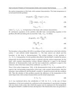
Figure 1 shows an example of a typical practical situation of a microstructure that may or
may not contain defects. In this case, the microstructure is an infinitely long cylinder, or
fiber. Together with the real sample, we show the 2D modelling we use to simulate this
situation and provide a 3D interpretation.
This basic design consists on an infinitely long metallic cylinder of diameter D, placed on a
flat substrate. We define two configurations: the Non-Perturbed Cylinder (NPC)
configuration, where the cylinder has no defect and the Perturbed Cylinder (PC)
configuration, which is a replica of the NPC except for a defect that can be either metallic or
dielectric and can be located either on the cylindrical microstructure itself or at its side, lying
on the flat substrate underneath. We consider the spatial profile of this defect to be
cylindrical, but other defect shapes can be considered without difficulty. The cylinder axis is
parallel to the Y direction and the X-Z plane corresponds to both the incidence and
scattering planes. This restricts the geometry to the two-dimensional case, which is adequate
for the purpose of our study [Valle et al., 1994; Moreno et al., 2006; Albella et al.,2006; Albella
et al., 2007]. The scattering system is illuminated by a monochromatic Gaussian beam of
wavelength λ (633nm) and width 2ω
0
, linearly polarized perpendicular to the plane of
incidence (S-polarized).
In order to account for the modifications introduced by the presence of a defect in the
scattering patterns of the whole system, we use the Extinction theorem, which is one of the
bases of modern theories developed for solving Maxwell’s Equations. The primary reason
for this choice is that it has been proven a reliable and effective method for solving 2D light-
scattering problems of rounded particles in close proximity to many kinds of substrates
[Nieto-Vesperinas et al., 1992; Sanchez-Gil et al., 1992; Ripoll et al., 1997; Saiz et al., 1996].
Detection and Characterization of Nano-Defects Located on
Micro-Structured Substrates by Means of Light Scattering
175
Fig. 1. Example of a contaminated microstructure (top figure) and its corresponding 2D and
3D models.
The Extinction theorem is a numerical algorithm. To perform the calculations, it is necessary
to discretize the entire surface contour profile (substrate, cylinder and defect) into an array
of segments whose length is much smaller than any other length scale of the system,
including the wavelength of light and the defect. Bear in mind that it is important to have a
partition fine enough to assure a good resolution in the high curvature regions of the surface
containing the lower portion of the cylinder and defect. Furthermore, and due to obvious
computing limitations, the surface has to be finite and the incident Gaussian beam has to be
wide enough to guarantee homogeneity in the incident beam but not so wide as to produce
undesirable edge effects at the end of the flat surface. Consequently, in our calculations, the
length of the substrate has been fixed to 80λ and the width (2ω
0
) of the Gaussian beam to 8λ.
3. Metallic substrates
In this section we initially discuss the case of metallic cylinders, or fibers, deposited on
metallic substrates and with the defect either on the cylinder itself or on the substrate but
near the cylinder.
Defect on the Cylinder
As a first practical situation, Figure 2 shows the backscattered intensity pattern, as a
function of the incident angle θ
i
, for a metallic cylinder of diameter D = 2λ. We consider two
different types of defect materials of either silver or glass and having diameter d = 0.15λ.
It can be seen how the backscattering patterns measured on the unperturbed side of the
cylinder (corresponding to θ
s
< 0) remain almost unchanged from the reference pattern. In
this case, we could say that the defect was hidden or shadowed by the incident beam. If the
scattering angle is such that the light illuminates the defect directly, a noticeable change in
the positions and intensity values of the maxima and minima results. The number of
maxima and minima observed may even change if the defect is larger than 0.4λ. This means
that there is no change in the effective size of the cylinder due to the presence of the defect.
This result can be explained using a phase-difference model [Nahm & Wolf, 1987; Albella et
al., 2007], where the substrate is replaced by an image cylinder located opposite the
Wave Propagation
176
substrate from the real one. Then, we can consider the two cylinders as two coherent
scatterers. The resultant backscattered field is the linear superposition of the scattered fields
from each cylinder, which only differ by a phase corresponding to the difference in their
optical paths and reflectance shifts. This phase difference is directly related to the diameter
of the cylinder. See the Appendix for more detail on this model.
Fig. 2. Backscattered intensity pattern I
back as a function of the incident angle θi for a metallic
cylinder of diameter D = 2λ. Two different types of defect material (either silver or glass)
have been considered, with a diameter d = 0.15λ [Albella et al., 2007].
One other interesting point is that the backscattering pattern has nearly the same shape in
terms of intensity values and minima positions, regardless of the nature of the defect.
Perhaps, the small differences observed manifest themselves better when the defect is
metallic. However for θ
s
> 0, a difference in the backscattered intensity can be noticed when
comparing the results for silver and glass defects. If we observe a minimum in close detail
(magnified regions), we see how I
back
increases with respect to the cylinder without the
defect when it is made of silver. In the case of glass located at the same position, I
back
decreases. These differences can be analyzed by considering an incremental integrated
backscattering parameter σ
br
, which is the topic of the next section.
Parameter σ
br
One of the objectives outlined in the introduction of this chapter was to show how the
backscattering pattern changes when the size and the position of a defect are changed, and
Detection and Characterization of Nano-Defects Located on
Micro-Structured Substrates by Means of Light Scattering
177
whether it is possible to find a relationship between those changes and the defect properties
of size and position. A systematic analysis of the pattern evolution is necessary. The
possibility of using the shift in the minima to obtain the required information [Peña et al.,
1999] is not suitable in this case because there is no consistency in the behaviour of the
angular positions of the minima with defect change. Based on the loss of symmetry in the
backscattering patterns introduced by the cylinder defect, a more suitable parameter can be
introduced to account for these variations. We have defined it as
σ
br
±
=
σ
b
±
−
σ
b 0
±
σ
b 0
±
=
σ
b
±
σ
b 0
±
−1
where
ssbackb
dI
θθσ
⋅=
∫
±
±
º90
0
)(
is the backscattering intensity (I
back
) integrated over either the positive (0º to 90º) or the
negative (0º to −90º) quadrant. Subscript 0 stands for the NPC configuration. One of the
reasons for using σ
br
±
is that integrating over θ
s
allows us to account for changes produced
by the defect in the backscattering efficiencies associated with an entire backscattering
quadrant, not just in a fixed direction.
Figure 3 shows a comparison of σ
br
calculated from the scattering patterns shown in Figure
2, as a function of the angular position of the defect on the main cylinder. It can be seen that
the maximum value of σ
br
±
has an approximate linear dependence on the defect size d. As an
example, for the case of a metallic defect near a D = 2λ cylinder, [σ
br
]
max
= 2.51d − 0.14 with a
regression coefficient of 0.99 and d expressed in units of λ. For d ∈ [0.05λ, 0.2λ] and cylinder
sizes comparable to λ, it is found that the positions [σ
br
]
max
and [σ
br
]
min
are independent of the
cylinder size D. Another characteristic of the evolution of σ
br
+
is the presence of a minimum
or a maximum around φ = 90º for metallic and dielectric defects, respectively. Examining
the behaviour of this minimum allows us to conclude that [σ
br
]
min
also changes linearly with
defect size; however, the slope is no longer independent of the cylinder size.
Fig. 3. σ
br
±
comparison for two different types of defects as a function of the defect position
for a silver cylinder of D = 2λ [Albella et al., 2007].
Wave Propagation
178
The most interesting feature shown in Figure 3 is that in all cases considered, σ
br
for a glass
defect has the opposite behaviour of that observed for a silver defect. That is, when the
behaviour of the dielectric is maximal, the behaviour of the conductor is minimal, and vice
versa. This behaviour suggests a way to discriminate metallic from dielectric defects. We
shall focus now on the evolution of parameter σ
±
with the optical properties of the defect
and in particular for a dielectric defect around the regions where the oscillating behaviour of
σ
br
reaches the maximum amplitude, that is, φ = 50º and φ = 90º.
Fig. 4. Evolution of σ
br
±
with ε for a fixed defect position (50º). The behaviour for the glass
defect (red) is opposite that of the silver defect (black) [Albella et al., 2007].
Figure 4, shows three curves of σ
br
+
(50º) as a function of the dielectric constant ε (ranging from
2.5 to 17), for three different defect sizes. For each defect size, σ
br
+
(50º) begins negative and with
negative slope; it reaches a minimum (-0.22) and then undergoes a transition to a positive
slope to a maximum (approximately 0.45). This means that for each size, there is a value of ε
large enough to produce values of σ
br
+
(50º) similar to those obtained for silver defects. The zero
value would correspond to a situation where σ
br
+
(50º) cannot be used to discriminate the
original defect. When the former analysis is repeated for φ = 90º similar behaviour is found,
although σ
br
+
(90º) has the opposite sign, as expected. As an example, σ
br
+
(90º) for a d = 0.1λ
defect is shown in Figure 4. Analogue calculations have been carried out for different values of
D ranging from λ to 2λ, leading to similar results, i.e., the same σ
br
(ε) with zero values is
obtained for different values of ε. The region shadowed in Figure 4, typically a glass defect, can
be fit linearly and could produce a direct estimation of the dielectric constant of the defect. As
an example, σ
br
(50º) = −0.03ε + 0.02 for the case of d = 0.1λ.
4. Defect on the substrate
We now consider the defect located on the substrate close to the main cylinder, within 1 or 2
wavelengths. In Figure 5 we see that there remains a clear difference in the backscattering
patterns obtained in each of the two hemispheres, thus making it possible to predict which
side of the cylinder the defect is located. Results shown in Figure 4 correspond to a cylinder
of D = 2λ and defect positions: x = 1.2λ, 2λ, while the defect size is fixed at d = 0.2λ.
Detection and Characterization of Nano-Defects Located on
Micro-Structured Substrates by Means of Light Scattering
179
Fig. 5. Backscattering patterns obtained for when the defect is located on the substrate,
together with the perfect, isolated cylinder case.
We observe again that the backscattering pattern changes more on the side where the defect
is located. This behaviour is similar to that observed in the case of a defect on the cylinder.
However, if we look at the side opposite the defect, the backscattering pattern does change if
the defect is located outside the shadow cast by the cylinder. When the defect is near the
cylinder (x = 1.2λ), that is, within the shadow region, the change in the scattering pattern is
negligible at any incident angle. Nevertheless, when the defect is located further from the
cylinder (x = 2λ), the change in the left-hand side can be noticed for incidences as large as
θ
i
= 40º.
Figure 6 shows the evolution of σ
br
for two different cylinders of D = 1λ and D = 2λ, and for
three different sized defects, d = 0.1λ, 0.15λ and 0.2λ. The shadowed area represents defect
positions beneath the cylinder, not considered in the calculations. The smaller shadow
produced in the D = λ case causes oscillations in σ
br
−
for smaller values of x.
It is worth noting that for a given cylinder size, the presence and location of a defect can be
monitored. For a D = λ cylinder with x as great as 2λ, σ
br
−
can increase as much as 10% for a
defect of d = 0.2λ. When the defect is closer than x = 1.5λ, σ
br
+
becomes negative while σ
br
−
is
not significant. Finally, when x < λ, σ
br
+
is very sensitive and strongly tends to zero. In the
case of a D = 2λ cylinder, the most interesting feature is the combination of high absolute
values and the strong oscillation of σ
br
+
for x within the interval [λ, 2λ]. Here the absolute
value of |σ
br
+
| indicates the proximity of the defect, and the sign designates the location
within the interval.
Although the size of the defect does not change the general behaviour, it is interesting to
notice that when comparing both cases, σ
br
+
is sensitive to the defect size and also dependent
on the size of the cylinder, something that did not occur in the former configuration when
the defect was located on the cylinder. Both situations can be considered as intrinsically
different scattering problems: with the defect on the substrate, there are two distinct
scattering particles, but with the defect on the cylinder, the defect is only modifying slightly
the shape of the cylinder and consequently the overall scattering pattern.
To illustrate this difference, Figure 7 shows some examples of the near-field and far-field
patterns produced by both situations for different defect positions. Figure 7(a) shows the
Wave Propagation
180
Fig. 6. σ
br
for two different cylinders sizes, D = λ, 2λ and three defect sizes d = 0.1λ, 0.15λ and
0.2λ. Defect position x ranges from 0.5λ to 3λ from the center of the Cylinder [Albella et al.,
2007].
near-field plot of the perfect cylinder and will be used as a reference. Figure 7(b) and 7(c)
correspond to the cases of a metallic defect on the cylinder. The outline of the defect is
visible on these panels. It can be seen that the defect does not change significantly the shape
of the near field when compared to the perfect cylinder case. Figure 7(d) and 7(e)
correspond to the cases of a metallic defect on the substrate. In Figure 7(d), the defect is
farthest from the cylinder, outside the shadow region, and we observe a significantly
different field distribution around the micron-sized particle located in what initially was a
maximum of the local field produced by the main cylinder. The same feature can be found
in the far-field plot. This case corresponds to the maximum change with respect to the non-
defect case. Finally, Figure 7(e) corresponds to the case of a metallic defect on the substrate
and close to the cylinder, very close to the position shown in Figure 7(c). As expected, both
cases are almost indistinguishable.
Detection and Characterization of Nano-Defects Located on
Micro-Structured Substrates by Means of Light Scattering
181
Fig. 7. (a) Near field plots for a silver cylinder sized D = 2λ located on a silver substrate and
illuminated at normal incidence. (b) and (c) show patterns for the defect located on the
cylinder and (d) and (e) show patterns for the defect located on the substrate. The main
cylinder and defect are outlined in black. Each plot has its corresponding far-field at the
bottom compared to the NPC case pattern.
Wave Propagation
182
5. Influence of the optical properties of the substrate
In this section, we discuss the sensitivity of the defect detection technique to the optical
properties of the substrate in the two possible situations described before: (A) with the
defect on the cylinder and (B) with the defect on the substrate near the cylinder. We will see
how the substrate can affect the detection capabilities in each particular situation.
In the previous sections, we described how a small defect located on a micron-sized silver
cylinder on a substrate changes the backscattered intensity. We showed that an integration
of the backscattered intensity over either the positive or negative quadrant, corresponding
to the defect side or the opposite side, yields a parameter σ
br
sensitive not only to the
existence of the defect but also to its size and location on the microstructure. These results
were initially obtained for perfectly conducting systems and later on, for more realistic
systems: dielectric or metallic defects on a metallic cylinder located on a metallic substrate.
From a practical point of view, detection and sizing of very small defects on microstructures
located on any kind of substrate by non-invasive methods could be very useful in quality-
control technology and in nano-scale monitoring processes. This section is focused on
examining the sensitivity of this technique to the optical properties of the substrate in the
aforementioned situations. In this section we also consider the cylinder to be composed of
gold.
5.1 Defect on the cylinder
Figure 8 shows a comparison between the backscattered intensity pattern for a perturbed
gold cylinder located on a metallic gold substrate and the backscattering pattern obtained
for the same system located on other substrates having different optical properties. The
diameter of the main cylinder and of the defect are D = λ and d = 0.1λ, respectively, thus
keeping constant the ratio d/D = 0.1. The defect position has been fixed on the cylinder at φ =
50º as it is one of the most representative cases.
As can be observed for backscattering angles θ
s
< 0, that is when the cylinder shadows the
defect, the shape of the pattern remains essentially the same. We also do see slightly smaller
values as we increase the dielectric constant of the substrate. When we illuminate the system
on the same side as the defect, θ
s
> 0, we tend to see the opposite behaviour: in the locations
where the values of I
back
increased as we increase the dielectric constant of the substrate, and
approaching the values of I
back
for the metallic substrate case. Although the changes in the
backscattering induced by the defect may seem negligible, we will see that these differences
can be monitored with appropriate integrating parameters. In particular, we use the
integrated backscattering parameter σ
br
as defined in the previous sections.
Figure 9(a) shows the behaviour of σ
br
for different dielectric substrates as a function of the
angular position of the defect. An interesting result is the increase of |σ
br
+
| as we increase ε,
reaching a maximum for the case of a metal. The opposite behaviour is observed for |σ
br
−
|.
The maximum absolute value of σ
br
+
and σ
br
−
for pure dielectric substrates is plotted in
Figure 9(b) as a function of the substrate dielectric constant ε. We notice that the quantity σ
br
is more sensitive to ε within the interval ε ∈ [1.2, 4] and it saturates for high values of ε,
tending to the metal substrate case. Absorption has not been considered for the case of real
dielectrics as it is very small in the visible range. Another interesting result is that for a
defect on the upper part of the cylinder φ < 50º, σ
br
−
is very sensitive to the metal/dielectric
nature of the substrate. On the other hand, these remarkable values of σ
br
−
make it more
difficult to locate the position of the defect.
Detection and Characterization of Nano-Defects Located on
Micro-Structured Substrates by Means of Light Scattering
183
Fig. 8. Backscattering patterns for a defect on a cylinder placed on a substrate for different
substrate optical properties (ε). The defect and cylinder are made of gold and of size d =0.1λ
and D=λ respectively.
Fig. 9. (a) Evolution of σ
br
for a defect on a cylinder as a function of the optical properties of
the substrate. (b) Evolution of max(σ
+
) and max(σ
−
) for pure dielectric substrates as a function
of the substrate dielectric constant, ε [Albella et al., 2008].
Wave Propagation
184
5.2 Defect on the substrate
Figure 10 shows a series of graphs comparing the patterns obtained for different dielectric
substrates with those obtained for a metallic substrate for a fixed defect position x = 3λ/4.
For θ
s
< 0, i.e. the region opposite to the defect side, the change induced by the defect in the
backscattering pattern is not significant, independent of the kind of substrate material.
However, when θ
s
> 0, the backscattering is strongly affected by the defect, especially for the
dielectric substrate. For increasing values of the dielectric constant, the change induced by
the defect becomes smaller. This is the opposite of what was found when the defect was on
the cylinder.
Fig. 10. The backscattered intensity pattern I
back
as a function of the incident angle θ
i
.
Parameter σ
br
allows for a straightforward assessment of these defects. Figure 11 shows the
evolution of σ
br
for different dielectric and metallic substrates as a function of the position x
of the defect in the substrate. The shadowed area represents defect positions under the
cylinder, not considered in the calculations. The most interesting feature of the curves
shown in Figure 11(a) is the high sensitivity of |σ
br
+
| to the presence of a defect for the case
of dielectric substrates. This sensitivity grows when the contrast in refractive index between
the defect and the substrate increases. The maxima of σ
br
+
and σ
br
−
are plotted in Figure 11(b)
as a function of ε for the dielectric substrate case. Both decrease and saturate for large values
of ε. It is also worth remarking that when the defect is on the substrate, σ
br
> 0, except for
some positions corresponding to the metallic substrate case. This means that, on average,
the backscattering is enhanced by a particle on the dielectric substrate, but it can be reduced
when the defect lies on a metallic substrate. However, when the defect is on the cylinder,
negative values are found for either kind of substrate.
Detection and Characterization of Nano-Defects Located on
Micro-Structured Substrates by Means of Light Scattering
185
Fig. 11. (a) Evolution of σ
br
as a function of the substrate optical properties. A defect lies on
the substrate. (b) Evolution of max(σ
+
) and max(σ
−
) for pure dielectric substrates as a function
of the substrate dielectric constant ε [Albella et al., 2008].
Fig. 12. Near-field plots corresponding to two different substrates illuminated at normal
incidence. The figures on the left correspond to the reference case having no defect and on
the right to a defect on the substrate. On the top are results for a dielectric substrate ε = 1.6
and on the bottom for a gold substrate ε = 11 + 1.5i.
Finally, to illustrate this enhancement, Figure 12 shows some examples of the near-field
pattern obtained for two different substrates illuminated at normal incidence. The figures on
Wave Propagation
186
the left correspond to the reference case having no defect and on the right to a defect on the
substrate. On the top are results for a dielectric substrate ε = 1.6 and on the bottom for a gold
substrate. We see that for low values of ε, we observe a new spatial distribution around the
micron-sized particle resulting in a new local maximum of intensity, which produces the
maximum change with respect to the non-defect case. This strong change in the near-field
distribution is not surprising since this defect position corresponds to a maximum in σ
br
+
as
observed in Figure 11(b). Near-field plots (Figure 12) show a close correlation among the
maxima located near the microstructure and the angular (φ) and linear (x) positions of the
maxima obtained for σ
br
plots.
6. Conclusion
The results in this chapter suggest that the measurement of σ
br
can be a useful means of
monitoring, sizing and characterizing small defects adhered to microstructures or
substrates. From a practical point of view, detection and sizing of very small defects on
microstructures by some reliable and non-invasive method is useful in quality control
technology. In this context, the objective was to study the sensitivity of this technique to the
optical properties of the substrate in two situations: (A) when the defect was located on a
cylinder and (B) when the defect was located on the substrate near a cylinder. We also have
anticipated how choosing the appropriate material for the substrate in each particular
situation can influence this detection. In this chapter a system structured at two different
levels has been analyzed by studying its scattering properties in the backscattering
direction.
A parameter σ
b
±
defined as the integration of the backscattered intensity over a given
quadrant is a quantitative measure of overall backscattering variations. It can be used, for
instance, by measuring the relative variation with respect to an initial system σ
br
±
as has
been discussed in this chapter, as a simple measure of asymmetry through |σ
b
+
- σ
b
−
|, or
through a backscattering asymmetry index 2|σ
b
+
− σ
b
−
|/(σ
b
+
− σ
b
−
), presumably suitable for
experimental situations. Parameter σ
b
itself can be experimentally obtained through different
configurations [Peña et al., 2000].
The potential uses of a parameter like σ
br
±
depend very much on the needs of the research
and on any previous knowledge. When applied to the double-cylinder case, the following
has been demonstrated:
i. With the defect on the cylinder, parameter σ
br
±
depends on the defect size and position,
while when the defect is on the substrate, σ
br
±
is also dependent on the main particle size
D;
ii. With the defect on the cylinder, its composition (metal/dielectric) may be identified
from the sign of σ
br
±
for a given defect position;
iii. A remarkable increase of σ
br
−
is characteristic of the defect being on the substrate and is
not found when the defect is on the principle particle;
iv. Strong oscillations in σ
br
+
observed when the defect is on the substrate for small values
of x can identify very precisely the position of the defect;
v. The use of metallic or dielectric substrates does not affect significantly the behaviour of
σ
br
and therefore does not present a limitation for this parameter.
This is not the first time that changes in the backscattering pattern obtained from a simple
configuration allows for the characterization of some geometrical or material changes
produced in the scattering object, but we think the procedure shown here is applicable to a
Detection and Characterization of Nano-Defects Located on
Micro-Structured Substrates by Means of Light Scattering
187
wide range of 2D structures whose defects often require rapid identification. Finally, these
results have a natural extension to 3D geometries that would enlarge the range of practical
situations and the scope of this work. This would require more powerful computing
techniques and tools applied over an extensive caustic. Everything shown in this chapter
can be seen as the basis for analyzing more complex geometrical systems.
7. Appendix
A particle sizing method is proposed using a double-interaction model (DIM) for the light
scattered by particles on substrates. This model, based on that proposed by Nahm and
Wolfe [Nahm & Wolfe, 1987], accounts for the reflection of both the incident and the
scattered beams and reproduces the scattering patterns produced by particles on substrates,
provided that the angle of incidence, the polarization and the isolated particle scattering
pattern are known.
In this context, we show the results obtained using a simple model to assess the effect of the
presence of a nano-defect on a microstructure located on a substrate. This three-object
system can be modeled with an extension of the double interaction model, which was
shown to be useful for obtaining the electric field scattered from a single particle resting on a
substrate. In this chapter, we extend that model in a 2D frame, to a system where there are
two metallic cylinders, one being a nano-defect lying on a micron-sized structure that rests
on a flat substrate. We also show how this simple model reproduces the scattering pattern
variations with respect to the defect-free system when compared to that given by an exact
method. It is important to remark that this model has two interesting features: (1)
Transparency, in that it is easy to understand the mechanisms involved in the scattering;
and (2) Easy numerical implementation that can lead to fast computation.
Model description
The system consists of an infinitely long metallic cylinder of radius R placed on a flat
substrate (see Figure 13) while another, much smaller, cylinder rests on top of the first. Both
cylinders are assumed metallic, and in our calculations we give them the properties of silver.
The cylinder axis is parallel to the Y direction, and the X-Z plane is the scattering plane. This
reduces the geometry to 2D. The model we propose in this work can be described as an
application of the DIM [Nahm & Wolfe, 1987] for normal incidence in two steps: (1) to the
large cylindrical microstructure located on the flat substrate and (2) to the small cylindrical
nano-defect, assuming that the underlying cylinder approximates a flat substrate for the
small cylinder. Of course, the accuracy of this second approximation improves as the ratio
r/R approaches zero. We shall limit our solution to the range 0 < r/R < 0.1.
The DIM is based on the standard T-matrix solution for the isolated scatterer at normal
incidence. Two contributions to the total scattered field are generated in any direction: the
light directly scattered from the particle, and that scattered and reflected off the substrate.
The latter is affected by a complex Fresnel coefficient, thus having its phase shifted because
of its additional path.
If we now consider the two-particle system, the total scattered far field at a fixed scattering
direction given by the scattering angle θ
s
is the coherent superposition of four contributions,
two of them due to the large cylinder and two due to the small one. Looking at Figure 13,
arrows labelled (1) and (3) represent the components directly scattered by the particles to
Wave Propagation
188
Fig. 13. Multiple interaction model for two structures illuminated at normal incidence. Inset
shows the flat substrate approximation and image theory applied to the defect.
the detector; and arrows labelled (2) and (4) correspond to the components scattered
downwards by the particles and then reflected towards the observation angle.
Simple calculations allow us to account for the phase shifts produced by the extra-path of
each contribution from a plane normal to the incidence direction to a plane normal to the
observation. Taking the direct contribution (3) as the reference beam having zero phase
(δ
3
= 0):
()
(
)
(
)
1
2.1cos
s
s
Rr
π
θ
δθ
λ
++
=− (A.1)
()
21
4.cos
s
s
r
π
θ
δθ δ
λ
=+
(A.2)
()
4
4. cos
s
s
R
π
θ
δθ
λ
=
(A.3)
where θ
s
is the scattering angle, R and r are the radii of the large and small cylinders
respectively, and λ is the incident wavelength. Reflection from the substrate is simplified
using the plane wave approximation and considering S-polarization, and is given by the
Fresnel reflection coefficient in its complex form,
()
()
()
2
2
ˆ
cos sin
ˆ
ˆ
cos sin
sub
s
sub
r
θ
εθ
θ
θ
εθ
−−
=
+−
(A.4)
The total scattered electric field under the assumptions of this Combined Double Interaction
Model (CDIM) is given by the sum of the four contributions,
Detection and Characterization of Nano-Defects Located on
Micro-Structured Substrates by Means of Light Scattering
189
()
(
)
()
11
10
. 180 .
i
o
ss
EAF e
φ
δ
θθ
⋅+
=− (A.5)
() () ()
()
22
20
.
s
i
sss
EAFre
φ
δα
θθθ
⋅++
=
(A.6)
()
(
)
3
30
. 180 .
i
o
ss
EAF e
φ
θθ
⋅
=−
(A.7)
() () ()
()
44
40
.
s
i
sss
EAFre
φ
δα
θθθ
⋅++
=
(A.8)
where A
0
is the amplitude of the incident beam, and the complex terms have been expressed
in their polar form, φ
i
is the Mie phase corresponding to the i
th
contribution, F(θ
s
) is the
amplitude of the scattered electric far field in the θ
s
direction for an isolated particle, which
are given by the T-matrix amplitudes applied to the case of a cylinder, and α
s
is the phase
introduced by the Fresnel reflection.
Testing the model
Results obtained by using the CDIM are compared with others obtained from the ET
method, which is an exact rendering of the Maxwell equations in their integral form. Figure
14 shows the scattering intensity patterns obtained from the CDIM approximation (top) and
from the ET (bottom) in semi-logarithmic scale. CDIM results have been shifted upwards for
an easy visualization. The continuous line plots correspond to the defect-free situation
(single cylinder) in all cases, while the dashed line corresponds to the case of a defect located
on the top of the cylinder.
In Figure 15 we consider the range of validity of this model. CDIM and ET are compared for
R = λ and for r = 0.05λ, 0.1λ and 0.15λ. We observe that both patterns show the same outer
minima positions for a defect/cylinder aspect ratio (r/R) up to 0.1, while for the case r/R=
0.15, distortions in the pattern become important. The CDIM reproduces the changes
produced in the lobed structure of the scattering patterns and particularly the minima
positions. If we look at Figure 14(a) as an example, we can see that in the case of the exact
solution (shown at the bottom part of the graph), there is a shift in the minima produced by
the presence of the defect, and this shift is accurately reproduced by the model.
One limit imposed on the ratio r/R is due to assuming the underlying main cylinder is flat.
For values of r/R < 0.1 the changes introduced by the real curvature in the Fresnel
coefficients and in the T-matrix scattering amplitude are very small and the changes in the
phase of the contribution due to the optical path difference are negligible as long as R is of
the order of the wavelength.
Although this problem may be overcome by numerically calculating the exact angular
reflections and paths, it is worthwhile to consider this model for its simplicity and
transparency. Because of its simplicity, the model can be extended to other situations, for
instance, a 3D implementation by introducing the Mie coefficients for spheres, different
contaminating particles, different defect locations, etc.
8. Acknowledgements
The authors wish to acknowledge the funds provided by the Ministry of Education of Spain
under project #FIS2007-60158. We also thank the computer resources provided by the
Spanish Supercomputing Network (RES) node at Universidad de Cantabria.
Wave Propagation
190
Fig. 14. Scattering patterns calculated using CDIM and ET for three different sizes of the
underlying cylinder, keeping a constant defect/cylinder aspect ratio of 0.1: (a). R = λ/2 and r
= λ/20; (b). R = λ and r = λ/10; (c). R = 1.5λ and r = 0.15λ. This corresponds with defect sizes
of 60, 120 and 180 nm for an incident wavelength of 0.6 μm [Albella et al., 2007].
Fig. 15. Scattering pattern of an R = λ cylinder with a defect of r = 0.05λ, 0.1λ and 0.15λ
calculated using CDIM (top) and ET (bottom) [Albella et al., 2007].
Detection and Characterization of Nano-Defects Located on
Micro-Structured Substrates by Means of Light Scattering
191
9. References
Albella, P., F. Moreno, J. M. Saiz, and F. González, “Monitoring small defects on surface
microstructures through backscattering measurements.” Opt. Lett. 31, 1744-1746,
(2006).
Albella, P., F. Moreno, J. M. Saiz, and F. González, “Backscattering of metallic
microstructures will small defects located on flat substrates.” Opt. Exp. 15, (2007)
6857–6867.
Albella, P., F. Moreno, J. M. Saiz, and F. González, “2D double interaction method for
modeling small particles contaminating microstructures located on substrates.” J.
Quant. Spectrosc. Radiative Trans. 106, 4–10 (2007).
Albella, P., F. Moreno, J. M. Saiz, and F. González, “Influence of the Substrate Optical
Properties on the backscattering of contaminated microstructures.” J. Quant.
Spectrosc. Radiative Trans. 109, (2008) 1339–1346.
Chen, H. T., R. Kersting and G. C. Cho, “Terahertz imaging with nanometer resolution.”
Appl. Phys. Lett. 83, (2003) 3.
Germer, T. A., and G. W. Mulholland. “Size metrology comparison between aerosol
electrical mobility and laser surface light scattering,” Characterization and
Metrology for ULSI Technology, (2005), 579–583.
Germer, T. A., “Light scattering by slightly non-spherical particles on surfaces,” Opt. Lett. 27,
1159-1161 (2002).
Johnson, B. R, “Light scattering from a spherical particle on a conducting plane, in normal
incidence,” J. Opt. Soc. Am. A 19, 11 (2002).
Lee, K. G., H. W. Kihm, J. E. Kihm, W. J. Choi, H. Kim, C. Ropers, D. J. Park, Y. C. Yoon, S. B.
Choi, D. H. Woo, J. Kim, B. Lee, Q. H. Park, C. Lienau, and D. S. Kim, “Vector field
microscopic imaging of light,” Nature Photonics 1, (2007) 53–56.
Liswith, M. L., E. J. Bawolek, and E. D. Hirleman, “Modeling of light scattering by
submicrometer spherical particles on silicon and oxidized silicon surfaces,” Opt.
Eng. 35, 858-869 (1996).
Mittal, K. L. (editor). Particles on surfaces: Detection, Adhesion and Removal. VSP, Utrech
(1999).
Moreno, F and F. González Eds. Light scattering from microstructures. Springer Verlag
(2000).
Moreno, F., F. González, and J. M. Saiz, “Plasmon spectroscopy of metallic nanoparticles
above flat dielectric substrates,” Opt. Lett., 31, (2006), 1902-1904.
Mulholland, G. W, T. A. Germer, and J. C. Stover, “Modeling, measurement and standards
for wafer inspection,” Proceedings of the Government Microcircuits Applications and
Critical Technologies. (2003), 1–4.
Nahm, K. B., and W. L. Wolfe, “Light-scattering models for spheres on a conducting plane,”
Appl. Opt. 26, (1987), 2995–2999.
Nieto-Vesperinas, M., and J. A. Sánchez-Gil, “Light scattering from a random rough
interface with total internal reflection,” J. Opt. Soc. Am. A 9, (1992) 424–436.
Peña, J.L., J. M. Saiz, P. Valle, F. González, and F. Moreno, “Tracking scattering minima to
size metallic particles on flat substrates,” Particle & Particle Systems Characterization
16, (1999) 113–118.
Ripoll, J., A. Madrazo, and M. Nieto-Vesperinas, “Scattering of electromagnetic waves from
a body over a random rough surface,” Opt. Comm. 142, (1997) 173–178.
Wave Propagation
192
Saiz, J.M., P. J. Valle, F. González, E. M. Ortiz, and F. Moreno, “Scattering by a metallic
cylinder on a substrate: burying effects,” Opt. Lett., 21, (1996) 1330–1332.
Sánchez-Gil, J. A., and M. Nieto-Vesperinas, “Resonance effects in multiple light scattering
from statistically rough metallic surfaces,” Phys. Rev. B 45 8623-8633 (1992).
Sonnichsen, C., B. M. Reinhard, J. Liphardt, and A. P. Alivisatos, “A molecular ruler based
on plasmon coupling of single gold and silver nanoparticles,” Nature Biotechnology
23, (2005), 741–745.
Stuart, D., A. J. Haes, C. R. Yonzon, E. Hicks, and R. V. Duyne, “Biological applications of
localised surface plasmonic phenomenae,” IEE Proc., Nanobiotechnology 152, (2005)
13–32.
Valle, P., F. González, and F. Moreno, “Electromagnetic wave scattering from conducting
cylindrical structures on flat substrates: study by means of the extinction theorem,”
Appl. Opt. 33, (1994), 512–523.
10
Nanofocusing of Surface Plasmons at the
Apex of Metallic Tips and at the Sharp
Metallic Wedges. Importance of
Electric Field Singularity
Andrey Petrin
Joint Institute for High Temperatures of Russian Academy of Science
Russia
1. Introduction
Nanofocusing of light is localization of electromagnetic energy in regions with dimensions
that are significantly smaller than the wavelength of visible light (of the order of one
nanometer). This is one of the central problems of modern near-field optical microscopy that
takes the resolution of optical imaging beyond the Raleigh’s diffraction limit for common
optical instruments [Zayats (2003), Pohl (1984), Novotny (1994), Bouhelier (2003), Keilmann
(1999), Frey (2002), Stockman (2004), Kawata (2001), Naber (2002), Babadjanyan (2000),
Nerkararyan (2006), Novotny (1995), Mehtani (2006), Anderson (2006)]. It is also important
for the development of new optical sensors and delivery of strongly localized photons to
tested molecules and atoms (for local spectroscopic measurements [Mehtani (2006),
Anderson (2006), Kneipp (1997), Pettinger (2004), Ichimura (2004), Nie (1997), Hillenbrand
(2002)]). Nanofocusing is also one of the major tools for efficient delivery of light energy
into subwavelength waveguides, interconnectors, and nanooptical devices [Gramotnev
(2005)].
There are two phenomena of exceptional importance which make it possible nanofocusing.
The first is the phenomenon of propagation with small attenuation of electromagnetic
energy of light along metal-vacuum or metal-dielectric boundaries. This propagation exists
in the form of strictly localized electromagnetic wave which rapidly decreases in the
directions perpendicular to the boundary. Remembering the quantum character of the
surface wave they say about surface plasmons and surface plasmon polaritons (SPPs) as
quasi-particles associated with the wave. The dispersion of the surface wave has the
following important feature [Economou (1969), Barnes (2006)]: the wavelength tends to zero
when the frequency of the SPPs tends to some critical (cut off) frequency above which the
SPPs cannot propagate. For SPPs propagating along metal-vacuum plane boundary this
critical frequency is equal to
2
p
ω
(we use Drude model without absorption in metal). For
spherical boundary this critical frequency [Bohren, Huffman (1983)] is equal to
3
p
ω
. So,
the SPP critical frequency depends on the form of the boundary. By changing the frequency
of SPPs it is possible to decrease the wavelength of the SPPs to the values substantially
Wave Propagation
194
smaller than the wavelength of visible light in vacuum and use the SPPs for trivial focusing
by creation a converging wave [Bezus (2010)]. In this case there is no breaking the diffraction
Raleigh’s limitation and the energy of the wave is focused into the region with dimensions
of the order of wavelength of the SPPs. These dimensions may be substantially smaller than
the wavelength of light in vacuum corresponding to the same frequency. As a result we
have nanofocusing of light energy. The second phenomenon is electrostatic electric field
strengthening at the apex of conducting tip (at the apex of geometrically ideal tip there is
electrostatic field singularity, i.e. the electrostatic field tends to infinity at the apex). This
phenomenon exists not only in electrostatics. For alternating electric field in the region with
the apex of the tip at the center (with dimensions smaller than wavelength) the quasi-static
approximation is applicable and there is a singularity of the time varying electric field (if the
frequency is low enough as we will see below). Surely, at the apex of a real tip there is no
singularity of electrostatic field since the apex is rounded. But near the apex the electric field
increases in accordance with power (negative) law of the singularity and the electric field
saturation at the apex is defined by the radius of the apex. This radius may be very small, of
the order of atomic size.
Nanofocusing of SPPs at the apex of metal tip is considered in [Stockman (2004), De Angelis
(2010)]. SPPs are created symmetrically at the basement of the tip and this surface wave
converges along the surface of the metal to the tip’s apex where surface wave energy is
focused. But conditions for existence of electric field singularity are considered in [Stockman
(2004), De Angelis (2010)] only for very sharp conical metal tips with small angle at the apex.
In [Petrin (2010)] it is shown that due to frequency dependence of metal permittivity in optic
frequency range the singularity of electric field at the tip’s of not very sharp apex may exist
in different forms.
The goal of the present chapter is investigation of the factors defined the type of
singular concentration of electromagnetic energy at the geometrically singular metallic
elements (such as apexes and edges) as one of the important condition for optimal
nanofocusing.
In the next sections of this chapter we discuss the following:
electric field singularities in the vicinity of metallic tip’s apex immersed into a uniform
dielectric medium;
electric field singularities in the vicinity of metallic tip’s apex touched a dielectric plate;
electric field singularities in the vicinity of edge of metallic wedge.
2. Nanofocusing of surface plasmons at the apex of metallic probe microtip.
Conditions for electric field singularity at the apex of microtip immersed into
a uniform dielectric medium.
In this section of the chapter we focus our attention on finding the condition for electric field
singularity of focused SPP electric field at the apex of a metal tip which is used as a probe in
a uniform dielectric medium. As we have discussed above this singularity is an important
feature of optimal SPP nanofocusing.
2.1 Condition for electric field singularity at the apex
Consider the cone surface of metal tip (see Fig. 1).
Nanofocusing of Surface Plasmons at the Apex of Metallic Tips
and at the Sharp Metallic Wedges. Importance of Electric Field Singularity
195
Fig. 1. Geometry of the problem.
Let calculate the electric field distribution near the tip’s apex. In spherical coordinates with
origin O at the apex and polar angle
θ
(see Fig. 1), an axially symmetric potential Ψ obeys
Laplace’s equation (we are looking for singular solutions, so in the vicinity of the apex the
quasistatic approximation for electric field is applicable)
2
1
sin
sin
r θ 0
rr θθ θ
∂∂Ψ ∂ ∂Ψ
⎛⎞ ⎛ ⎞
+
=
⎜⎟ ⎜ ⎟
∂∂ ∂ ∂
⎝⎠ ⎝ ⎠
.
Representing the solution as
(
)
Ψ rf
α
θ
= , where
α
is a constant parameter, we have
()
sin 1 sin
f
θ f θ
θθ
αα
∂
∂
⎛⎞
=− +
⎜⎟
∂∂
⎝⎠
.
Changing to the function g defined by the relation
(
)
(
)
cosfg
θ
θ
=
, which entails
sin
cos
df dg
θ
dθ d
θ
=−
,
we obtain Legendre’s differential equation
()
()
2
2
2
1cos 2cos 1 0
cos
cos
dg dg
g
d
d
θθαα
θ
θ
−
−++=.
It’s solution is the Legendre polynomial
(
)
cosP
α
θ
of degree
α
, which can be conveniently
represented as
()
1cos
cos , 1,1,
2
PF
α
θ
θαα
−
⎛⎞
=− +
⎜⎟
⎝⎠
,
where
F is the hypergeometric function. This representation is equally valid whether
α
is
integer or not.