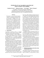
Báo cáo hóa học: "Fabrication of a Highly Sensitive Chemical Sensor Based on ZnO Nanorod Arrays" doc
Bạn đang xem bản rút gọn của tài liệu. Xem và tải ngay bản đầy đủ của tài liệu tại đây (528.17 KB, 7 trang )
NANO EXPRESS
Fabrication of a Highly Sensitive Chemical Sensor Based on ZnO
Nanorod Arrays
Jae Young Park
•
Sun-Woo Choi
•
Sang Sub Kim
Received: 24 June 2009 / Accepted: 29 October 2009 / Published online: 18 November 2009
Ó to the authors 2009
Abstract We report a novel method for fabricating a
highly sensitive chemical sensor based on a ZnO nanorod
array that is epitaxially grown on a Pt-coated Si substrate,
with a top–top electrode configuration. To practically test
the device, its O
2
and NO
2
sensing properties were inves-
tigated. The gas sensing properties of this type of device
suggest that the approach is promising for the fabrication of
sensitive and reliable nanorod chemical sensors.
Keywords ZnO nanorod array Á Chemical sensor Á
MOCVD
Recently, nanostructures, such as nanorods and nanowires,
made of semiconducting materials have been extensively
investigated for the purpose of using their unique proper-
ties in various nanoscale functional devices [1, 2]. For
instance, ZnO nanostructures have received particular
attention due to their many valuable properties and the ease
with which ZnO can be made into various nanostructure
shapes by many different methods [3–6].
Since nanorods and nanowires have much larger sur-
face-to-volume ratios compared to their thin film and bulk
material counterparts, their application to miniaturized
highly sensitive chemical sensors has been predicted to be
promising [7, 8]. The electrical and chemical sensing
properties of single ZnO nanorods have been extensively
investigated in recent years by the fabrication and testing of
single nanorod field-effect transistors (FETs). According to
the results, ZnO nanorods show an n-type semiconducting
behavior and their electrical transport is strongly dependent
on the adsorption and/or desorption nature of chemical
species [9–13]. Despite significant achievements in the
realization of chemical sensors based on single ZnO
nanorods [14–17], there still remain many aspects that
should be overcome before their actual application. Firstly,
the fabrication of sensors based on individual nanorods
involves a careful lithography process in which each fab-
rication step is expensive and tedious. Secondly, a precise
system that can measure currents in the region of 10
-9
Ais
necessary to detect the small current changes that occur in
a single nanorod during the adsorption/desorption of
chemical species. Finally, the slightly different sizes of
each nanorod and the different natures of the electrical
contacts in each sensor cause poor reproducibility.
In order to overcome the disadvantages of single nano-
rod chemical sensors, recently the use of vertically aligned
nanorod arrays (NRAs) in chemical sensors has been
attempted [18–20]. In these works, metal electrodes were
simply deposited on top of nanorod arrays using sputtering
[18, 20] or aerosol spray pyrolysis [19]. However, this
approach is likely to result in not distinctive but gradient
interfaces between nanorods and metal electrodes, possibly
deteriorating sensor efficiency. Therefore, an approach for
fabricating chemical sensors based on ZnO nanorod arrays
(NRAs) using more reliable electrode configurations needs
to be developed.
In this work, we report a novel approach to fabricating
chemical sensors based on ZnO NRAs with a top–top
electrode configuration. The approach used a coating and
etching process with a photoresist (PR). The results show
that the proposed ZnO NRA-based chemical sensor
exhibits a comparable sensitivity, a higher reproducibility
and can be made in a simpler way, suggesting that the
J. Y. Park Á S W. Choi Á S. S. Kim (&)
School of Materials Science and Engineering, Inha University,
Incheon 402-751, Korea
e-mail:
123
Nanoscale Res Lett (2010) 5:353–359
DOI 10.1007/s11671-009-9487-3
proposed approach is promising for fabricating chemical
sensors based on ZnO NRAs.
ZnO NRAs were synthesized on Pt-coated Si (001)
substrates using a horizontal-type metal organic chemical
vapor deposition (MOCVD) system without using any
metal catalyst. Pt films of *120 nm in thickness were
deposited on Si (001) substrates by a sputtering method.
Before the Pt deposition, a Ti interlayer of *5nm in
thickness was deposited on the bare Si substrates using the
same sputtering method. This was done in order to enhance
the adhesion of the Pt films to the Si substrates. According
to the high-resolution X-ray diffraction (XRD) results
(which are not presented here), the resultant 120-nm-thick
Pt films possessed a (111) preferred orientation normal to
the substrate plane, while showing a random alignment in
the in-plane direction. ZnO NRAs were grown at 500°C for
30 min using O
2
and diethylzinc as precursors with argon
as a carrier gas. The pressure in the reactor was kept at
5 torr. The flow rates of the oxygen and diethylzinc were
fixed to result in an O/Zn precursor ratio of 68. The
microstructures and crystalline quality of the synthesized
ZnO NRAs were investigated using field-emission
Fig. 1 Schematic (left) and real
(right) images on fabrication of
a ZnO NRA sensor. a As-
synthesized ZnO NRA on a Pt-
coated Si (001) substrate. b ZnO
NRA filled and coated with
positive PR. c Exposure of the
tip-ends of ZnO nanorods by
etching with inductively
coupled plasma in oxygen
atmosphere. d Deposition of Ni
(* 500 nm)/Au (* 50 nm)
metal layers by thermal
evaporation using a mask and
subsequent removal of
remaining PR by dipping in
acetone. The inset in the right
part of d shows a bird-view of
the electrode part
354 Nanoscale Res Lett (2010) 5:353–359
123
scanning electron microscopy (SEM) and high-resolution
transmission electron microscopy (TEM). The growth
behavior, alignment nature, substrate dependency, size and
shape control, fabrication of the field-effect transistors, and
the temperature-dependent electrical transport of the single
ZnO nanorods used in this study have been reported in
detail in our previous works [21–24].
Figure 1 displays the schematic (left) and real (right)
images in sequence on fabrication of chemical sensors in
this study using the synthesized ZnO NRAs. The images of
an as-synthesized ZnO NRA on a Pt-coated Si (001) sub-
strate are shown in Fig. 1a. For the device fabrication, the
NRA was synthesized partly on the substrate using a mask.
Positive photoresist (PR) was spread on the surface of the
ZnO NRA by a spin coater. As seen in Fig. 1b, a uniform
and smooth PR layer was formed. The space between
individual ZnO nanorods was completely filled with PR.
Next, a small portion of the PR layer was removed by
etching with inductively coupled plasma in oxygen atmo-
sphere. This consequently resulted in exposure of the tip-
ends of ZnO nanorods (see Fig. 1c). Then, using a mask of
2mm9 3 mm in area, Ni (*500 nm in thickness) and Au
(*50 nm) were sequentially deposited on the exposed tip-
ends by thermal evaporation, as shown in Fig. 1d. Finally,
the PR filled into the space between nanorods as well as
remained on the substrate was removed by dipping into
acetone. Then the sample was dried into a vacuum oven at
100°C. Note that the well-defined interface between the
nanorods and the electrode layer was formed, as shown in
the right part of Fig. 1d. The inset figure shows a bird-view
of the electrode part. It shows a continuous, well-defined
electrode layer.
As a practical test for ZnO NRA chemical sensor, the
sensing properties for O
2
and NO
2
were investigated. The
fabricated NRA chemical sensor was introduced into a
vacuum chamber equipped with a system that can measure
current and voltage by changing O
2
and NO
2
environments
using N
2
as a carrier gas. HP 4140B pA Meter/DC voltage
source was used as the measurement tool, which was
interfaced with a personal computer through a general
purpose interface bus (GPIB) card. The chamber pressure
was controlled using a gate valve and verified using an ion
gauge. The sensor assembly was heated to the desired
temperature by using a halogen lamp, and temperature was
monitored through a thermocouple. In this study, the
sensing measurement was performed at 573 K. The base
pressure of the vacuum chamber, which was connected to a
turbomolecular pump, was typically *5 9 10
-6
torr.
Using mass flow controllers, O
2
and NO
2
environments
were monitored.
As shown in a field-emission SEM image displayed in
Fig. 1, vertically well-aligned ZnO nanorods grew over the
Pt/Ti/Si (001) substrate. The nanorods are uniform in
diameter and length. It is clear that a continuous ZnO
interfacial layer exists. Our previous work on the early
growth stages of ZnO nanoneedles on sapphire (0001)
revealed that a continuous ZnO layer coherently strained to
the substrate grows first [25]. On top of the existing con-
tinuous layer, aligned nanoneedles start to form as the
growth proceeds further. A similar growth behavior
Fig. 2 a Bright-field TEM
image observed at the interface
between a ZnO NRA and a
substrate. Note that existence of
a continuous ZnO film of
150 nm in thickness on the Pt
layer. b Selected area electron
diffraction pattern taken from a
region including the Pt layer,
ZnO layer, and ZnO NRA.
c High-resolution TEM lattice
image taken at an interfacial
area of the ZnO layer and Pt
layer. d High-resolution TEM
lattice image of individual ZnO
nanorods
Nanoscale Res Lett (2010) 5:353–359 355
123
appears to occur during the growth of the ZnO NRAs on
Pt-coated Si substrates. The Ni/Au double layer that is
deposited on the tip-ends of the ZnO nanorods shows a
well-defined interface and the formation of a continuous
layer. To further investigate the microstructure of the ZnO
NRAs, TEM studies were carried out.
Figure 2a is a bright-field TEM image taken at the
interfacial area between the ZnO NRAs and the substrate.
The presence of the ZnO layer is more evident in this image.
Figure 2b is a selected area electron diffraction pattern of
the ZnO nanorods. This shows their alignment with the
(0001) planes parallel to the substrate surface. High-
resolution TEM lattice images of the interfacial layer and
ZnO nanorods are shown in Fig. 2c, d, respectively. These
images show perfect lattice arrays without any considerable
dislocations or stacking faults, meaning that the interfacial
ZnO layer is of an epitaxial quality and that the individual
ZnO nanorods are actually defect-free single crystals.
To practically test the NRA chemical sensor with the
top–top electrode configuration, its sensing properties
under O
2
and NO
2
environments were investigated. Fig-
ure 3a displays the current–voltage (I–V) curves obtained
for various O
2
concentrations. Note that for clarity, only
some of the results are presented. These I–V curves are
linear, indicating ohmic contact nature for the sensing
device in O
2
environments. In general, the conductivity in
semiconducting oxide sensors shows strong dependency on
the oxygen pressure, following the relationship [26]
r ¼ A expðÀE
A
=KTÞP
1=m
O
2
ð1Þ
where r is the electrical conductance, E
A
is the activation
energy for atomic diffusion around the grain boundary, A is
the pre-exponential factor, K is the gas constant, and T is
the temperature in Kelvin. The inset of Fig. 3a shows the
plot of log r versus log P
O
2
. The slope was -1/2.85,
indicating that m =-0.35. In case of p-type conduction, m
is positive. On the other hand, it is negative for n-type
conduction. Therefore, n-type conduction is operating in
the ZnO NRA at the various O
2
pressures. The value of m
relies on the dominating defects related to the sensing
mechanism.
The dynamic testing of a sensing device provides useful
information about the sensitivity, the response and recov-
ery times, and the reproducibility. Note that as described
before, the dynamic testing was performed in the vacuum
chamber. Pumping away oxygen or NO
2
has been per-
formed when ‘‘gas off’’ is indicated in Figs. 3, 4, and 5.
Figure 3b shows typical response curves of a ZnO NRA
chemical sensor to oxygen gas. When the sensor is exposed
to oxygen gas, the resistance sharply increases. When the
oxygen supply is stopped, the resistance quickly drops to a
low value. In order to mention the response and recovery
times more clearly, we have to wait for sufficient time and
the steady state resistance in oxygen and without oxygen,
i.e., saturated state. The resistance curves in Fig. 3b show
no saturation. However, the amounts of the resistance
change until the initiation of ‘‘gas off’’ were over 90%
compared with the saturated values. Thus, although the
data show no saturation, it is possible to mention the
response and recovery times because they are usually
defined as the time required to reach 90% of the final
equilibrium value of the sensor signals. Based on this, the
response and recovery times were 120–180 and 100–120 s,
respectively, depending on the O
2
concentration. It should
be noted that the sensor responses were very stable and
reproducible for the repeated test cycles. The superior
stability and reproducibility come from the fact that the
sensing response is the average value from an enormous
number of individual nanorods, unlike the sensing response
for a single nanorod chemical sensor. For the NRA
chemical sensor fabricated with the top–top electrode
configuration, considering the total area of the two top
Fig. 3 a I–V behavior of a ZnO NRA chemical sensor measured at
different O
2
concentrations. The inset shows a plot of resistance as a
function of O
2
concentration. b Typical response curves to various O
2
concentrations
356 Nanoscale Res Lett (2010) 5:353–359
123
electrodes is 12 mm
2
, the diameters of the nanorods are
*100 nm, and the gaps between them are *100 nm, then
*4 9 10
8
nanorods participate in the sensing process.
Figure 4a shows the change in resistance as a function
of time with different O
2
concentrations ranging from 1.4
to 500 ppm. Six cycles were successively recorded. As
shown, the device recovery was reproducible for all O
2
concentrations. The gas sensitivity (S) was estimated using
the relationship, S = ((R - R
0
)/R
0
), where R
0
is the initial
resistance in the absence of O
2
gas and R is the resistance
measured in the presence of O
2
gas. Figure 4b shows the
sensitivities extracted from Fig. 4a as a function of O
2
concentration. The sensitivity at an O
2
concentration of
1.4 ppm is 0.15, which is similar to the values previously
reported for oxygen sensors based on single ZnO nanorods
[27]. A linear relationship is obtained between sensitivity
and O
2
concentration in the O
2
concentration range, as
shown in Fig. 4b. The sensitivity of a semiconducting
oxide is usually depicted as S = A[C]
N
? B, where A and
B are constants and [C] is the concentration of the target
gas or vapor [28]. In the present study, the data fitting
results in S = 0.0059 [C] ? 0.323 for the NRA chemical
sensor. R
2
in the figure represents the quality of the curve
fit. Figure 4c shows the dependence of resistance by
Fig. 4 a Resistance change in a ZnO NRA chemical sensor measured
at different O
2
concentrations. b Sensitivity versus O
2
concentration.
c Dynamic resistance changes by successive increase in O
2
concentration
Fig. 5 a Resistance change in a ZnO NRA chemical sensor measured
at different NO
2
concentrations. b Sensitivity versus NO
2
concentra-
tion. The inset summarizes the response and recovery times with NO
2
concentration
Nanoscale Res Lett (2010) 5:353–359 357
123
successive increase in O
2
concentration. The resistance
quickly responds to the change in O
2
concentration. The
increased resistance to O
2
again increases by exposure to
more O
2
concentration. This behavior further confirms that
the fabricated sensor in this study can be used in the
environment with dynamically changing O
2
concentration.
In addition to the O
2
sensing properties of the NRA
sensor, its NO
2
sensing properties were investigated. Fig-
ure 5a shows the sensing cycles of the NRA sensor mea-
sured at 1–5 ppm NO
2
. As shown, the sensor well responds
to the introduction and removal of NO
2
as low as 1 ppm.
The sensitivity of the sensor to NO
2
is summarized in
Fig. 5b. The linear slope gives the equation of S = 0.018
[C] ? 0.047. The inset of Fig. 5b displays the response and
recovery times of the NRA sensor to NO
2
gas of various
concentrations. The response time is about 50 s and shows
no considerable difference depending on NO
2
concentra-
tion. In contrast, the recovery time prolongs from about 55
to 200 s with increasing NO
2
concentration from 1 to
5 ppm. The prolonged recovery time with higher gas
concentrations is often observed [29–31].
In case of n-type semiconductors like ZnO, oxidizing
gas such as O
2
or NO
2
mainly act as an electron accepter in
the surface reactions, and the width of electron depletion
layers is widened, leading to an increased resistance of the
sensors. O
2
or NO
2
molecules adsorbed on the surface of
ZnO layers take electrons from them, eventually leading to
surface depletion in ZnO. Conversely, the release of elec-
trons occurs in desorption of O
2
or NO
2
. This charge
transfer accounts for the resistance change observed in the
NRA sensor. The sensing results in this study demonstrate
that the approach proposed in this study is promising for
the fabrication of highly sensitive chemical sensors.
In summary, we have described a novel approach to
chemical sensors based on aligned ZnO NRAs grown on
Pt-coated Si substrates with a top–top electrode configu-
ration. The O
2
and NO
2
sensing properties of the fabricated
sensor showed both a high sensitivity and an excellent
reproducibility during the repeated test cycles. The results
show that the device proposed in this study is promising for
use as a highly sensitive, reliable chemical sensor.
Acknowledgments This work was supported by the Korea
Research Foundation Grant funded by the Korean Government
(MOEHRD, Basic Research Promotion Fund) (KRF-2008-521-
D00177).
References
1. S M. Lukas, M D. Judith, ZnO–nanostructures, defects, and
devices. Mater. Today 10, 40–48 (2007)
2. Z.L. Wang, Oxide nanobelts and nanowires-growth, properties,
and applications. J. Nanosci. Nanotechnol. 8, 27–55 (2008)
3. G D. Yuan, W J. Zhang, J S. Jie, X. Fan, J X. Tang, I. Shafiq,
Z Z. Ye, C S. Lee, S T. Lee, Tunable n-type conductivity and
transport properties of Ga-doped ZnO nanowire arrays. Adv.
Mater. 20, 168–173 (2008)
4. S.Y. Bae, C.W. Na, J.H. Kang, J. Park, Comparative structure and
optical properties of Ga-, In-, and Sn-doped ZnO nanowires
synthesized via thermal evaporation. J. Phys. Chem. B. 109,
2526–2531 (2005)
5. D.H. Kim, S.D. Lee, K.K. Kim, G.S. Park, J.M. Lee, S.W. Kim,
Free-standing ZnO nanorods and nanowalls by aqueous solution
method. J. Nanosci. Nanotechnol. 8, 4688–4691 (2008)
6. Y.S. Yun, J.Y. Park, H. Oh, J J. Kim, S.S. Kim, Electrical
transport properties of size-tuned ZnO nanorods. J. Mater. Res.
21, 132–136 (2005)
7. Q. Wan, Q.H. Li, Y.J. Chen, T.H. Wang, X.L. He, J.P. Li, C.L.
Lin, Fabrication and ethanol sensing characteristics of ZnO
nanowire gas sensors. Appl. Phys. Lett. 84, 3654–3656 (2004)
8. Z.L. Wang, FUNCTIONAL OXIDE NANOBELTS: materials,
properties and potential applications in nanosystems and bio-
technology. Annu. Rev. Phys. Chem. 55, 159–196 (2004)
9. Q.H. Li, T. Gao, Y.G. Wang, T.H. Wang, Adsorption and
desorption of oxygen probed from ZnO nanowire films by pho-
tocurrent measurements. Appl. Phys. Lett. 86, 123117–123119
(2005)
10. X.J. Hung, Y.K. Choi, Chemical sensors based on nanostructured
materials. Sens. Actuators B 122, 659–671 (2007)
11. C.C. Li, Z.F. Du, L.M. Li, H.C. Yu, Q. Wan, T.H. Wang, Sur-
face-depletion controlled gas sensing of ZnO nanorods grown at
room temperature. Appl. Phys. Lett. 91, 032101–032103 (2007)
12. R. Ghosh, M. Dutta, D. Basak, Self-seeded growth and ultraviolet
photoresponse properties of ZnO nanowire arrays. Appl. Phys.
Lett. 91, 073108–073110 (2007)
13. Y. Qiu, S. Yang, Nanotetrapods: Controlled vapor-phase syn-
thesis and application for humidity sensing. Adv. Funct. Mater.
17, 1345–1352 (2007)
14. Z. Fan, J.G. Lu, Gate-refreshable nanowire chemical sensors.
Appl. Phys. Lett. 86, 123510–123512 (2005)
15. K. Keem, J. Kang, C. Yoon, D Y. Jeong, B M. Moon, S. Kim,
Enhanced performance of ZnO nanowire field effect transistors
by H
2
annealing. Jpn. J. Appl. Phys. 46, 6230–6232 (2007)
16. W. Wang, H.D. Xiong, M.D. Edelstein, D. Gundlach, J.S. Suehle,
C.A. Richter, Low frequency noise characterizations of ZnO
nanowire field effect transistors. J. Appl. Phys. 101, 044313–
044317 (2007)
17. F.V. Farmakis, T. Speliotis, K.P. Alexandrou, C. Tsamis, M.
Kompitsas, I. Fasaki, P. Jedrasik, G. Petersson, B. Nilsson, Field-
effect transistors with thin ZnO as active layer for gas sensor
applications. Microelectron. Eng. 85, 1035–1038 (2008)
18. H.T. Wang, B.S. Kang, F. Ren, L.C. Tien, P.W. Sadik, D.P.
Norton, S.J. Pearton, J. Lin, Hydrogen-selective sensing at room
temperature with ZnO nanorods. Appl. Phys. Lett. 86, 243503–
243505 (2005)
19. P. Parthangal, R. Cavicchi, M. Zachariah, A universal approach
to electrically connecting nanowire arrays using nanoparticles—
application to a novel gas sensor architecture. Nanotechnology
17, 3786–3790 (2006)
20. J.X. Wang, X.W. Sun, Y. Yang, H. Huang, Y.C. Lee, O.K. Tan,
L. Vayssieres, Hydrothermally grown oriented ZnO nanorod
arrays for gas sensing applications. Nanotechnology 17, 4995–
4998 (2006)
21. J.Y. Park, D.J. Lee, S.S. Kim, Size control of ZnO nanorod arrays
grown by metalorganic chemical vapour deposition. Nanotech-
nology 16, 2044–2047 (2005)
22. J.Y. Park, Y.S. Yun, Y.S. Hong, H. Oh, J J. Kim, S.S. Kim,
Synthesis, electrical and photoresponse properties of vertically
358 Nanoscale Res Lett (2010) 5:353–359
123
well-aligned and epitaxial ZnO nanorods on GaN-buffered sap-
phire substrates. Appl. Phys. Lett. 87, 123108–123110 (2005)
23. J.Y. Park, D.J. Lee, Y.S. Yun, J.H. Moon, B.T. Lee, S.S. Kim, J.
Cryst, Temperature-induced morphological changes of ZnO
grown by metalorganic chemical vapor deposition. Growth 276,
158–164 (2005)
24. J.Y. Park, H. Oh, J J. Kim, S.S. Kim, The temperature-dependent
electrical transport mechanism of single ZnO nanorods. Nano-
technology 17, 1255–1259 (2006)
25. J.Y. Park, J.M. Lee, J.H. Je, S.S. Kim, J. Cryst, Early stage
growth behavior of ZnO nanoneedle arrays on Al
2
O
3
(0001)by
metalorganic chemical vapor deposition. Growth 281, 446–451
(2005)
26. Y. Xu, X. Zhou, O.T. Sorensen, Oxygen sensors based on
semiconducting metal oxides: an overview. Sens. Actuators B 65,
2–4 (2000)
27. Z. Fan, D. Wang, P.C. Chang, W.Y. Tseng, J.G. Lu, ZnO
nanowire field-effect transistor and oxygen sensing property.
Appl. Phys. Lett. 85, 5923–5925 (2004)
28. P.T. Moseley, B.C. Tofield, Solid State Gas Sensors (Adam
Hilger, Bristol, 1987)
29. F. Naso, F. Babudri, D. Colangiuli, G.M. Farinola, F. Quaranta,
R. Rella, R. Tafuro, L. Valli, Thin film construction and char-
acterization and gas-sensing performances of a tailored pheny-
lene-thienylene copolymer. J. Am. Chem. Soc. 125, 9055–9061
(2003)
30. J. Li, Y. Lu, Q. Ye, M. Cinke, J. Han, M. Meyyappan, Carbon
nanotube sensors for gas and organic vapor detection. Nano Lett.
3, 929–933 (2003)
31. M. Penza, R. Rossi, M. Alvisi, G. Gassano, M.A. Signore, E.
Serra, R. Giorgi, Pt- and Pd-nanoclusters functionalized carbon
nanotubes networked films for sub-ppm gas sensors. Sens.
Actuators B 135, 289–297 (2008)
Nanoscale Res Lett (2010) 5:353–359 359
123