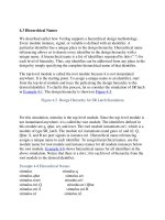
Verilog Programming part 12 pps
Bạn đang xem bản rút gọn của tài liệu. Xem và tải ngay bản đầy đủ của tài liệu tại đây (42.13 KB, 6 trang )
5.2 Gate Delays
Until now, we described circuits without any delays (i.e., zero delay). In real
circuits, logic gates have delays associated with them. Gate delays allow the
Verilog user to specify delays through the logic circuits. Pin-to-pin delays can also
be specified in Verilog. They are discussed in Chapter 10
, Timing and Delays.
5.2.1 Rise, Fall, and Turn-off Delays
There are three types of delays from the inputs to the output of a primitive gate.
Rise delay
The rise delay is associated with a gate output transition to a 1 from another value.
Fall delay
The fall delay is associated with a gate output transition to a 0 from another value.
Turn-off delay
The turn-off delay is associated with a gate output transition to the high impedance
value (z) from another value.
If the value changes to x, the minimum of the three delays is considered.
Three types of delay specifications are allowed. If only one delay is specified, this
value is used for all transitions. If two delays are specified, they refer to the rise
and fall delay values. The turn-off delay is the minimum of the two delays. If all
three delays are specified, they refer to rise, fall, and turn-off delay values. If no
delays are specified, the default value is zero. Examples of delay specification are
shown in Example 5-10
.
Example 5-10 Types of Delay Specification
// Delay of delay_time for all transitions
and #(delay_time) a1(out, i1, i2);
// Rise and Fall Delay Specification.
and #(rise_val, fall_val) a2(out, i1, i2);
// Rise, Fall, and Turn-off Delay Specification
bufif0 #(rise_val, fall_val, turnoff_val) b1 (out, in, control);
Examples of delay specification are shown below.
and #(5) a1(out, i1, i2); //Delay of 5 for all transitions
and #(4,6) a2(out, i1, i2); // Rise = 4, Fall = 6
bufif0 #(3,4,5) b1 (out, in, control); // Rise = 3, Fall = 4, Turn-off = 5
5.2.2 Min/Typ/Max Values
Verilog provides an additional level of control for each type of delay mentioned
above. For each type of delay—rise, fall, and turn-off—three values, min, typ, and
max, can be specified. Any one value can be chosen at the start of the simulation.
Min/typ/max values are used to model devices whose delays vary within a
minimum and maximum range because of the IC fabrication process variations.
Min value
The min value is the minimum delay value that the designer expects the gate to
have.
Typ val
The typ value is the typical delay value that the designer expects the gate to have.
Max value
The max value is the maximum delay value that the designer expects the gate to
have.
Min, typ, or max values can be chosen at Verilog run time. Method of choosing a
min/typ/max value may vary for different simulators or operating systems. (For
Verilog-XL™, the values are chosen by specifying options +maxdelays,
+typdelays, and +mindelays at run time. If no option is specified, the typical delay
value is the default). This allows the designers the flexibility of building three
delay values for each transition into their design. The designer can experiment with
delay values without modifying the design.
Examples of min, typ, and max value specification for Verilog-XL are shown in
Example 5-11
.
Example 5-11 Min, Max, and Typical Delay Values
// One delay
// if +mindelays, delay= 4
// if +typdelays, delay= 5
// if +maxdelays, delay= 6
and #(4:5:6) a1(out, i1, i2);
// Two delays
// if +mindelays, rise= 3, fall= 5, turn-off = min(3,5)
// if +typdelays, rise= 4, fall= 6, turn-off = min(4,6)
// if +maxdelays, rise= 5, fall= 7, turn-off = min(5,7)
and #(3:4:5, 5:6:7) a2(out, i1, i2);
// Three delays
// if +mindelays, rise= 2 fall= 3 turn-off = 4
// if +typdelays, rise= 3 fall= 4 turn-off = 5
// if +maxdelays, rise= 4 fall= 5 turn-off = 6
and #(2:3:4, 3:4:5, 4:5:6) a3(out, i1,i2);
Examples of invoking the Verilog-XL simulator with the command-line options
are shown below. Assume that the module with delays is declared in the file test.v.
//invoke simulation with maximum delay
> verilog test.v +maxdelays
//invoke simulation with minimum delay
> verilog test.v +mindelays
//invoke simulation with typical delay
> verilog test.v +typdelays
5.2.3 Delay Example
Let us consider a simple example to illustrate the use of gate delays to model
timing in the logic circuits. A simple module called D implements the following
logic equations:
out = (a b) + c
The gate-level implementation is shown in Module D (Figure 5-8
). The module
contains two gates with delays of 5 and 4 time units.
Figure 5-8. Module D
The module D is defined in Verilog as shown in Example 5-12.
Example 5-12 Verilog Definition for Module D with Delay
// Define a simple combination module called D
module D (out, a, b, c);
// I/O port declarations
output out;
input a,b,c;
// Internal nets
wire e;
// Instantiate primitive gates to build the circuit
and #(5) a1(e, a, b); //Delay of 5 on gate a1
or #(4) o1(out, e,c); //Delay of 4 on gate o1
endmodule
This module is tested by the stimulus file shown in Example 5-13
.
Example 5-13 Stimulus for Module D with Delay
// Stimulus (top-level module)
module stimulus;
// Declare variables
reg A, B, C;
wire OUT;
// Instantiate the module D
D d1( OUT, A, B, C);
// Stimulate the inputs. Finish the simulation at 40 time units.
initial
begin
A= 1'b0; B= 1'b0; C= 1'b0;
#10 A= 1'b1; B= 1'b1; C= 1'b1;
#10 A= 1'b1; B= 1'b0; C= 1'b0;
#20 $finish;
end
endmodule
The waveforms from the simulation are shown in Figure 5-9
to illustrate the effect
of specifying delays on gates. The waveforms are not drawn to scale. However,
simulation time at each transition is specified below the transition.
1. The outputs E and OUT are initially unknown.
2. At time 10, after A, B, and C all transition to 1, OUT transitions to 1 after a
delay of 4 time units and E changes value to 1 after 5 time units.
3. At time 20, B and C transition to 0. E changes value to 0 after 5 time units,
and OUT transitions to 0, 4 time units after E changes.
Figure 5-9. Waveforms for Delay Simulation
It is a useful exercise to understand how the timing for each transition in the above
waveform corresponds to the gate delays shown in Module D.
[ Team LiB ]
[ Team LiB ]
5.3 Summary
In this chapter, we discussed how to model gate-level logic in Verilog. We also
discussed different aspects of gate-level design.
• The basic types of gates are and, or, xor, buf, and not. Each gate has a logic
symbol, truth table, and a corresponding Verilog primitive. Primitives are
instantiated like modules except that they are predefined in Verilog. The
output of a gate is evaluated as soon as one of its inputs changes.
• Arrays of built-in primitive instances and user-defined modules can be
defined in Verilog.
• For gate-level design, start with the logic diagram, write the Verilog
description for the logic by using gate primitives, provide stimulus, and look
at the output. Two design examples, a 4-to-1 multiplexer and a 4-bit full
adder, were discussed. Each step of the design process was explained.
• Three types of delays are associated with gates: rise, fall, and turn-off.
Verilog allows specification of one, two, or three delays for each gate.
Values of rise, fall, and turn-off delays are computed by Verilog, based on
the one, two, or three delays specified.
• For each type of delay, a minimum, typical, and maximum value can be
specified. The user can choose which value to apply at simulation time. This
provides the flexibility to experiment with three delay values without
changing the Verilog code.
• The effect of propagation delay on waveforms was explained by the simple,
two-gate logic example. For each gate with a delay of t, the output changes t
time units after any of the inputs change.