Verilog Programming part 9 potx
Bạn đang xem bản rút gọn của tài liệu. Xem và tải ngay bản đầy đủ của tài liệu tại đây (46.72 KB, 9 trang )
4.3 Hierarchical Names
We described earlier how Verilog supports a hierarchical design methodology.
Every module instance, signal, or variable is defined with an identifier. A
p
articular identifier has a unique place in the design hierarchy. Hierarchical name
referencing allows us to denote every identifier in the design hierarchy with a
unique name. A hierarchical name is a list of identifiers separated by dots (".") for
each level of hierarchy. Thus, any identifier can be addressed from any place in the
design by simply specifying the complete hierarchical name of that identifier.
The top-level module is called the root module because it is not instantiated
anywhere. It is the starting point. To assign a unique name to an identifier, start
from the top-level module and trace the path along the design hierarchy to the
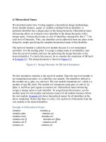
desired identifier. To clarify this process, let us consider the simulation of SR latch
in Example 4-1
. The design hierarchy is shown in Figure 4-5.
Figure 4-5. Design Hierarchy for SR Latch Simulation
For this simulation, stimulus is the top-level module. Since the top-level module is
not instantiated anywhere, it is called the root module. The identifiers defined in
this module are q, qbar, set, and reset. The root module instantiates m1, which is a
module of type SR_latch. The module m1 instantiates nand gates n1 and n2. Q,
Qbar, S, and R are port signals in instance m1. Hierarchical name referencing
assigns a unique name to each identifier. To assign hierarchical names, use the
module name for root module and instance names for all module instances below
the root module. Example 4-8
shows hierarchical names for all identifiers in the
above simulation. Notice that there is a dot (.) for each level of hierarchy from the
root module to the desired identifier.
Example 4-8 Hierarchical Names
stimulus stimulus.q
stimulus.qbar stimulus.set
stimulus.reset stimulus.m1
stimulus.m1.Q stimulus.m1.Qbar
stimulus.m1.S stimulus.m1.R
stimulus.n1 stimulus.n2
Each identifier in the design is uniquely specified by its hierarchical path name. To
display the level of hierarchy, use the special character %m in the $display task.
See Table 3-4
, String Format Specifications, for details.
[ Team LiB ]
[ Team LiB ]
4.4 Summary
In this chapter, we discussed the following aspects of Verilog:
• Module definitions contain various components. Keywords module and
endmodule are mandatory. Other components—port list, port declarations,
variable and signal declarations, dataflow statements, behavioral blocks,
lower-level module instantiations, and tasks or functions—are optional and
can be added as needed.
• Ports provide the module with a means to communicate with other modules
or its environment. A module can have a port list. Ports in the port list must
be declared as input, output, or inout. When instantiating a module, port
connection rules are enforced by the Verilog simulator. An ANSI C style
embeds the port declarations in the module definition statement.
• Ports can be connected by name or by ordered list.
• Each identifier in the design has a unique hierarchical name. Hierarchical
names allow us to address any identifier in the design from any other level
of hierarchy in the design.
[ Team LiB ]
[ Team LiB ]
4.5 Exercises
1:
What are the basic components of a module? Which components are
mandatory?
2:
Does a module that does not interact with its environment have any I/O
p
orts? Does it have a port list in the module definition?
3:
A 4-bit parallel shift register has I/O pins as shown in the figure below.
Write the module definition for this module shift_reg. Include the list of
p
orts and port declarations. You do not need to show the internals.
4:
Declare a top-level module stimulus. Define REG_IN (4 bit) and CLK (1
bit) as reg register variables and REG_OUT (4 bit) as wire. Instantiate the
module shift_reg and call it sr1. Connect the ports by ordered list.
5:
Connect the ports in Step 4 by name.
6:
Write the hierarchical names for variables REG_IN, CLK, and
REG_OUT.
7:
Write the hierarchical name for the instance sr1. Write the hierarchical
names for its ports clock and reg_in.
[ Team LiB ]
[ Team LiB ]
5.1 Gate Types
A logic circuit can be designed by use of logic gates. Verilog supports basic logic
gates as predefined primitives. These primitives are instantiated like modules
except that they are predefined in Verilog and do not need a module definition. All
logic circuits can be designed by using basic gates. There are two classes of basic
gates: and/or gates and buf/not gates.
5.1.1 And/Or Gates
And/or gates have one scalar output and multiple scalar inputs. The first terminal
in the list of gate terminals is an output and the other terminals are inputs. The
output of a gate is evaluated as soon as one of the inputs changes. The and/or gates
available in Verilog are shown below.
and or xor
nand nor xnor
The corresponding logic symbols for these gates are shown in Figure 5-1
. We
consider gates with two inputs. The output terminal is denoted by out. Input
terminals are denoted by i1 and i2.
Figure 5-1. Basic Gates
These gates are instantiated to build logic circuits in Verilog. Examples of gate
instantiations are shown below. In Example 5-1
, for all instances, OUT is
connected to the output out, and IN1 and IN2 are connected to the two inputs i1
and i2 of the gate primitives. Note that the instance name does not need to be
specified for primitives. This lets the designer instantiate hundreds of gates without
giving them a name.
More than two inputs can be specified in a gate instantiation. Gates with more than
two inputs are instantiated by simply adding more input ports in the gate
instantiation (see Example 5-1
). Verilog automatically instantiates the appropriate
gate.
Example 5-1 Gate Instantiation of And/Or Gates
wire OUT, IN1, IN2;
// basic gate instantiations.
and a1(OUT, IN1, IN2);
nand na1(OUT, IN1, IN2);
or or1(OUT, IN1, IN2);
nor nor1(OUT, IN1, IN2);
xor x1(OUT, IN1, IN2);
xnor nx1(OUT, IN1, IN2);
// More than two inputs; 3 input nand gate
nand na1_3inp(OUT, IN1, IN2, IN3);
// gate instantiation without instance name
and (OUT, IN1, IN2); // legal gate instantiation
The truth tables for these gates define how outputs for the gates are computed from
the inputs. Truth tables are defined assuming two inputs. The truth tables for these
gates are shown in Table 5-1
. Outputs of gates with more than two inputs are
computed by applying the truth table iteratively.
Table 5-1. Truth Tables for And/Or Gates
5.1.2 Buf/Not Gates
Buf/not gates have one scalar input and one or more scalar outputs. The last
terminal in the port list is connected to the input. Other terminals are connected to
the outputs. We will discuss gates that have one input and one output.
Two basic buf/not gate primitives are provided in Verilog.
buf not
The symbols for these logic gates are shown in Figure 5-2
.
Figure 5-2. Buf and Not Gates
These gates are instantiated in Verilog as shown Example 5-2
. Notice that these
gates can have multiple outputs but exactly one input, which is the last terminal in
the port list.
Example 5-2 Gate Instantiations of Buf/Not Gates
// basic gate instantiations.
buf b1(OUT1, IN);
not n1(OUT1, IN);
// More than two outputs
buf b1_2out(OUT1, OUT2, IN);
// gate instantiation without instance name
not (OUT1, IN); // legal gate instantiation
sum = (a b cin)
cout = (a b) + cin (a b)
The logic diagram for a 1-bit full adder is shown in Figure 5-6
.
Figure 5-6. 1-bit Full Adder
This logic diagram for the 1-bit full adder is converted to a Verilog description,
shown in Example 5-7
.
Example 5-7 Verilog Description for 1-bit Full Adder
// Define a 1-bit full adder
module fulladd(sum, c_out, a, b, c_in);
// I/O port declarations
output sum, c_out;
input a, b, c_in;
// Internal nets
wire s1, c1, c2;
// Instantiate logic gate primitives
xor (s1, a, b);
and (c1, a, b);
xor (sum, s1, c_in);
and (c2, s1, c_in);
xor (c_out, c2, c1);
endmodule
A 4-bit ripple carry full adder can be constructed from four 1-bit full adders, as
shown in Figure 5-7
. Notice that fa0, fa1, fa2, and fa3 are instances of the module
fulladd (1-bit full adder).
Figure 5-7. 4-bit Ripple Carry Full Adder
This structure can be translated to Verilog as shown in Example 5-8
. Note that the
p
ort names used in a 1-bit full adder and a 4-bit full adder are the same but they
represent different elements. The element sum in a 1-bit adder is a scalar quantity
and the element sum in the 4-bit full adder is a 4-bit vector quantity. Verilog keeps
names local to a module. Names are not visible outside the module unless
hierarchical name referencing is used. Also note that instance names must be
specified when defined modules are instantiated, but when instantiating Verilog
p
rimitives, the instance names are optional.
Example 5-8 Verilog Description for 4-bit Ripple Carry Full Adder
// Define a 4-bit full adder
module fulladd4(sum, c_out, a, b, c_in);
// I/O port declarations
output [3:0] sum;
output c_out;
input[3:0] a, b;
input c_in;
// Internal nets
wire c1, c2, c3;
// Instantiate four 1-bit full adders.
fulladd fa0(sum[0], c1, a[0], b[0], c_in);
fulladd fa1(sum[1], c2, a[1], b[1], c1);
fulladd fa2(sum[2], c3, a[2], b[2], c2);
fulladd fa3(sum[3], c_out, a[3], b[3], c3);
endmodule
Finally, the design must be checked by applying stimulus, as shown in Example 5-
9. The module stimulus stimulates the 4-bit full adder by applying a few input
combinations and monitors the results.
Example 5-9 Stimulus for 4-bit Ripple Carry Full Adder
// Define the stimulus (top level module)
module stimulus;
// Set up variables
reg [3:0] A, B;
reg C_IN;
wire [3:0] SUM;
wire C_OUT;
// Instantiate the 4-bit full adder. call it FA1_4
fulladd4 FA1_4(SUM, C_OUT, A, B, C_IN);
// Set up the monitoring for the signal values
initial
begin
$monitor($time," A= %b, B=%b, C_IN= %b, C_OUT= %b, SUM= %b\n",
A, B, C_IN, C_OUT, SUM);
end
// Stimulate inputs
initial
begin
A = 4'd0; B = 4'd0; C_IN = 1'b0;
#5 A = 4'd3; B = 4'd4;
#5 A = 4'd2; B = 4'd5;
#5 A = 4'd9; B = 4'd9;
#5 A = 4'd10; B = 4'd15;
#5 A = 4'd10; B = 4'd5; C_IN = 1'b1;
end
endmodule
The output of the simulation is shown below.
0 A= 0000, B=0000, C_IN= 0, C_OUT= 0, SUM= 0000
5 A= 0011, B=0100, C_IN= 0, C_OUT= 0, SUM= 0111
10 A= 0010, B=0101, C_IN= 0, C_OUT= 0, SUM= 0111
15 A= 1001, B=1001, C_IN= 0, C_OUT= 1, SUM= 0010
20 A= 1010, B=1111, C_IN= 0, C_OUT= 1, SUM= 1001
25 A= 1010, B=0101, C_IN= 1,, C_OUT= 1, SUM= 0000