Parallel Programming: for Multicore and Cluster Systems- P9 pps
Bạn đang xem bản rút gọn của tài liệu. Xem và tải ngay bản đầy đủ của tài liệu tại đây (244.58 KB, 10 trang )
70 2 Parallel Computer Architecture
leading to a large number of cache misses and therefore a large execution time. This
phenomenon is also called thrashing.
2.7.1.4 Fully Associative Caches
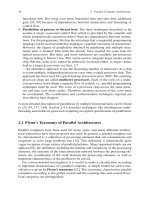
In a fully associative cache, each memory block can be placed in any cache position,
thus overcoming the disadvantage of direct mapped caches. As for direct mapped
caches, a memory address can again be partitioned into a block address (s leftmost
bits) and a word address (w rightmost bits). Since each cache block can contain any
memory block, the entire block address must be used as tag and must be stored with
the cache block to allow the identification of the memory block stored. Thus, each
memory address is partitioned as follows:
To check whether a given memory block is stored in the cache, all the entries
in the cache must be searched, since the memory block can be stored at any cache
position. This is illustrated in Fig. 2.33(b).
w
block address word address
tag
s
The advantage of fully associative caches lies in the increased flexibility when
loading memory blocks into the cache. The main disadvantage is that for each mem-
ory access all cache positions must be considered to check whether the correspond-
ing memory block is currently held in the cache. To make this search practical,
it must be done in parallel using a separate comparator for each cache position,
thus increasing the required hardware effort significantly. Another disadvantage is
that the tags to be stored for each cache block are significantly larger as for direct
mapped caches. For the example cache introduced above, the tags must be 30 bits
long for a fully associated cache, i.e., for each 32-bit memory block, a 30-bit tag
must be stored. Because of the large search effort, a fully associative mapping is
useful only for caches with a small number of positions.
2.7.1.5 Set Associative Caches
Set associative caches are a compromise between direct mapped and fully asso-
ciative caches. In a set associative cache, the cache is partitioned into v sets
S
0
, ,S
v−1
where each set consists of k = m/v blocks. A memory block B
j
is
not mapped to an individual cache block, but to a unique set in the cache. Within the
set, the memory block can be placed in any cache block of that set, i.e., there are k
different cache blocks in which a memory block can be stored. The set of a memory
block B
j
is defined as follows:
B
j
is mapped to set S
i
, if i = j mod v
2.7 Caches and Memory Hierarchy 71
tag
tag
tag
tag
blocktag
43210
memory address
processor
compare
B
0
1
B
2
B
3
B
B
0
1
B
B
15
cache hit
s − r
rw
cache
data
w
s
replace
s + w
main memory
cache miss
(a)
tag
tag
tag
tag
compare
B
0
1
B
2
B
3
B
B
0
1
B
B
15
cache hit
w
cache
data
cache miss
w
s
replace
s + w
main memory
43210
memory address
processor
tag
s
w
(b)
compare
B
0
1
B
B
15
tag
tag
tag
tag
B
0
1
B
2
B
3
B
0
S
S
1
w
s
replace
s + w
main memory
43210
memory address
processor
s − d
d
s − d s − d
w
cache
data
}
}
cache hit
cache miss
(c)
settag
Fig. 2.33 Illustration of the mapping of memory blocks to cache blocks for a cache with m = 4
cache blocks (r = 2) and a main memory with n = 16 memory blocks (s = 4). Each block
contains two memory words (w = 1). (a) Direct mapped cache; (b) fully associative cache; (c)set
associative cache with k = 2 blocks per set, using v = 2sets(d = 1)
This
figure
will be
printed
in b/w
72 2 Parallel Computer Architecture
for j = 0, ,n − 1. A memory access is illustrated in Fig. 2.33(c). Again, a
memory address consists of a block address (s bits) and a word address (w bits).
The d = log v rightmost bits of the block address determine the set S
i
to which
the corresponding memory block is mapped. The leftmost s − d bits of the block
address are the tag that is used for the identification of the memory blocks stored
in the individual cache blocks of a set. Thus, each memory address is partitioned as
follows:
w
block address word address
set numbertag
ds − d
When a memory access occurs, the hardware first determines the set to which
the memory block is assigned. Then, the tag of the memory block is compared with
the tags of all cache blocks in the set. If there is a match, the memory access can be
performed via the cache. Otherwise, the corresponding memory block must first be
loaded into one of the cache blocks of the set.
For v = m and k = 1, a set associative cache reduces to a direct mapped cache.
For v = 1 and k = m, a fully associative cache results. Typical cases are v = m/4
and k = 4, leading to a 4-way set associative cache, and v = m/8 and k = 8,
leading to an 8-way set associative cache. For the example cache, using k = 4 leads
to 4K sets; d = 12 bits of the block address determine the set to which a memory
block is mapped. The tags used for the identification of memory blocks within a set
are 18 bits long.
2.7.1.6 Block Replacement Methods
When a cache miss occurs, a new memory block must be loaded into the cache.
To do this for a fully occupied cache, one of the memory blocks in the cache must
be replaced. For a direct mapped cache, there is only one position at which the new
memory block can be stored, and the memory block occupying that position must be
replaced. For a fully associative or set associative cache, there are several positions
at which the new memory block can be stored. The block to be replaced is selected
using a replacement method. A popular replacement method is least recently used
(LRU) which replaces the block in a set that has not been used for the longest time.
For the implementation of the LRU method, the hardware must keep track for
each block of a set when the block was used last. The corresponding time entry
must be updated at each usage time of the block. This implementation requires
additional space to store the time entries for each block and additional control logic
to update the time entries. For a 2-way set associative cache the LRU method can be
implemented more easily by keeping a USE bit for each of the two blocks in a set.
When a cache block of a set is accessed, its USE bit is set to 1 and the USE bit of the
other block in the set is set to 0. This is performed for each memory access. Thus,
2.7 Caches and Memory Hierarchy 73
the block whose USE bit is 1 has been accessed last, and the other block should be
replaced if a new block has to be loaded into the set. An alternative to LRU is least
frequently used (LFU) which replaces the block of a set that has experienced the
fewest references. But the LFU method also requires additional control logic since
for each block a counter must be maintained which must be updated for each mem-
ory access. For a larger associativity, an exact implementation of LRU or LFU as
described above is often considered as too costly [84], and approximations or other
schemes are used. Often, the block to be replaced is selected randomly, since this can
be implemented easily. Moreover, simulations have shown that random replacement
leads to only slightly inferior performance compared to more sophisticated methods
like LRU or LFU [84, 164].
2.7.2 Write Policy
A cache contains a subset of the memory blocks. When the processor issues a write
access to a memory block that is currently stored in the cache, the referenced block
is definitely updated in the cache, since the next read access must return the most
recent value. There remains the question: When is the corresponding memory block
in the main memory updated? The earliest possible update time for the main mem-
ory is immediately after the update in the cache; the latest possible update time
for the main memory is when the cache block is replaced by another block. The
exact replacement time and update method is captured by the write policy. The most
popular policies are write-through and write-back.
2.7.2.1 Write-Through Policy
Using write-through, a modification of a block in the cache using a write access
is immediately transferred to main memory, thus keeping the cache and the main
memory consistent. An advantage of this approach is that other devices like I/O
modules that have direct access to main memory always get the newest value of
a memory block. This is also important for multicore systems, since after a write
by one processor, all other processors always get the most recently written value
when accessing the same block. A drawback of write-through is that every write
in the cache causes also a write to main memory which typically takes at least
100 processor cycles to complete. This could slow down the processor if it had
to wait for the completion. To avoid processor waiting, a write buffer can be used
to store pending write operations into the main memory [137, 84]. After writing
the data into the cache and into the write buffer, the processor can continue its
execution without waiting for the completion of the write into the main mem-
ory. A write buffer entry can be freed after the write into main memory com-
pletes. When the processor performs a write and the write buffer is full, a write
stall occurs, and the processor must wait until there is a free entry in the write
buffer.
74 2 Parallel Computer Architecture
2.7.2.2 Write-Back Policy
Using write-back, a write operation to a memory block that is currently held in
the cache is performed only in the cache; the corresponding memory entry is not
updated immediately. Thus, the cache may contain newer values than the main
memory. The modified memory block is written to the main memory when the
cache block is replaced by another memory block. To check whether a write to main
memory is necessary when a cache block is replaced, a separate bit (dirty bit) is held
for each cache block which indicates whether the cache block has been modified or
not. The dirty bit is initialized to 0 when a block is loaded into the cache. A write
access to a cache block sets the dirty bit to 1, indicating that a write to main memory
must be performed when the cache block is replaced.
Using write-back policy usually leads to fewer write operations to main memory
than write-through policy, since cache blocks can be written multiple times before
they are written back to main memory. The drawback of write-back is that the main
memory may contain invalid entries, and hence I/O modules can access main mem-
ory only through the cache.
If a write to a memory location goes to a memory block that is currently not
in the cache, most caches use the write-allocate method: The corresponding mem-
ory block is first brought into the cache and then the modification is performed as
described above. An alternative approach is write no allocate, which modifies in
main memory without loading it into the cache. However, this approach is used less
often.
2.7.2.3 Number of Caches
So far, we have considered the behavior of a single cache which is placed between
the processor and main memory and which stores data blocks of a program in exe-
cution. Such caches are also called data caches.
Besides the program data, a processor also accesses instructions of the program
in execution before they are decoded and executed. Because of loops in the program,
an instruction can be accessed multiple times. To avoid multiple loading operations
from main memory, instructions are also held in cache. To store instructions and
data, a single cache can be used (unified cache). But often, two separate caches are
used on the first level, an instruction cache to store instructions and a separate data
cache to store data. This approach is also called split caches. This enables a greater
flexibility for the cache design, since the data and instruction caches can work inde-
pendently of each other and may have different size and associativity depending on
the specific needs.
In practice, multiple levels of caches are typically used as illustrated in Fig. 2.34.
The current standard is to have two levels with a trend toward three levels. For
the first level (L1), split caches are typically used; for the remaining levels, unified
caches are standard. The caches are hierarchically organized, and for two levels, the
L1 caches contain a subset of the L2 cache which contains a subset of the main
memory.
The caches are normally integrated into the chip area of the processor. Typical
cache sizes lie between 8 Kbytes and 128 Kbytes for the L1 cache and between
2.7 Caches and Memory Hierarchy 75
Fig. 2.34 Illustration of a
two-level cache hierarchy
processor
instruction
cache
L1 data
cache
L2 cache
main
memory
256 Kbytes and 8 Mbytes for the L2 cache. Typical sizes of the main memory lie
between 1 Gbyte and 16 Gbytes. Typical access times are one or a few processor
cycles for the L1 cache, between 15 and 25 cycles for the L2 cache, between 100
and 1000 cycles for the main memory, and between 10 and 100 million cycles for
the hard disc [137].
2.7.3 Cache Coherency
Using a memory hierarchy with multiple levels of caches can help to bridge large
access times to main memory. But the use of caches introduces the effect that
memory blocks can be held in multiple copies in caches and main memory, and
after an update in the L1 cache, other copies might become invalid, in particular
if a write-back policy is used. This does not cause a problem as long as a single
processor is the only accessing device. But if there are multiple accessing devices,
as is the case for multicore processors, inconsistent copies can occur and should be
avoided, and each execution core should always access the most recent value of a
memory location. The problem of keeping the different copies of a memory location
consistent is also referred to as cache coherency problem.
In a multiprocessor system with different cores or processors, in which each pro-
cessor has a separate local cache, the same memory block can be held as copy in
the local cache of multiple processors. If one or more of the processors update a
copy of a memory block in their local cache, the other copies become invalid and
contain inconsistent values. The problem can be illustrated for a bus-based system
with three processors [35] as shown in the following example.
Example We consider a bus-based SMP system with three processors P
1
, P
2
, P
3
where each processor P
i
has a local cache C
i
for i = 1, 2, 3. The processors are
connected to a shared memory M via a central bus. The caches C
i
useawrite-
through strategy. We consider a variable u with initial value 5 which is held in the
main memory before the following operations are performed at times t
1
, t
2
, t
3
, t
4
:
t
1
: Processor P
1
reads variable u. The memory block containing u is loaded
into cache C
1
of P
1
.
t
2
: Processor P
3
reads variable u. The memory block containing u is also
loaded into cache C
3
of P
3
.
t
3
: Processor P
3
writes the value 7 into u. This new value is also written into
the main memory because write-through is used.
t
4
: Processor P
1
reads u by accessing the copy in its local cache.
76 2 Parallel Computer Architecture
At time t
4
, processor P
1
reads the old value 5 instead of the new value 7, i.e., a cache
coherency problem occurs. This is the case for both write-through and write-back
caches: For write-through caches, at time t
3
the new value 7 is directly written into
the main memory by processor P
3
, but the cache of P
1
will not be updated. For
write-back caches, the new value of 7 is not even updated in main memory, i.e., if
another processor P
2
reads the value of u after time t
3
, it will obtain the old value,
even when the variable u is not held in the local cache of P
2
.
For a correct execution of a parallel program on a shared address space, it must
be ensured that for each possible order of read and write accesses performed by
the participating processors according to their program statements, each processor
obtains the right value, no matter whether the corresponding variable is held in cache
or not.
The behavior of a memory system for read and write accesses performed by
different processors to the same memory location is captured by the coherency of
the memory system. Informally, a memory system is coherent if for each memory
location any read access returns the most recently written value of that memory
location. Since multiple processors may perform write operations to the same mem-
ory location at the same time, we must first define more precisely what the most
recently written value is. For this definition, the order of the memory accesses in
the parallel program executed is used as time measure, not the physical point in
time at which the memory accesses are executed by the processors. This makes the
definition independent of the specific execution environment and situation.
Using the program order of memory accesses, a memory system is coherent, if
the following conditions are fulfilled [84]:
1. If a processor P writes into a memory location x at time t
1
and reads from
the same memory location x at time t
2
> t
1
and if between t
1
and t
2
no other
processor performs a write into x, then P obtains at time t
2
the value written by
itself at time t
1
. Thus, for each processor the order of the memory accesses in its
program is preserved despite a parallel execution.
2. If a processor P
1
writes into a memory location x at time t
1
and if another pro-
cessor P
2
reads x at time t
2
> t
1
, then P
2
obtains the value written by P
1
,if
between t
1
and t
2
no other processors write into x and if the period of time t
2
−t
1
is sufficiently large. Thus, a value written by one of the processors must become
visible to the other processors after a certain amount of time.
3. If two processors write into the same memory location x, these write operations
are serialized so that all processors see the write operations in the same order.
Thus, a global write serialization is performed.
To be coherent, a memory system must fulfill these three properties. In particu-
lar, for a memory system with caches which can store multiple copies of memory
blocks, it must be ensured that each processor has a coherent view of the memory
system through its local caches. To ensure this, hardware-based cache coherence
protocols are used. Depending on the architecture of the execution platform, differ-
ent protocols are used, including snooping protocols and directory-based protocols.
2.7 Caches and Memory Hierarchy 77
2.7.3.1 Snooping Protocols
The technique of bus snooping has first been used for bus-based SMP systems,
where the local caches of the processors use a write-through policy. The technique
relies on the property that on such systems all memory accesses are performed via
the central bus, i.e., the bus is used as broadcast medium. Thus, all memory accesses
can be observed by the cache controllers of all processors. Each cache controller can
observe the memory accesses transferred over the bus. When the cache controller
observes a write into a memory location that is currently held in the local cache, it
updates the value in the cache by copying the new value from the bus into the cache.
Thus, the local caches always contain the most recently written values of memory
locations. These protocols are also called update-based protocols, since the cache
controllers directly perform an update. There are also invalidation-based protocols
in which the cache block corresponding to a memory block is invalidated so that
the next read access must perform an update from main memory first. Using an
update-based protocol in the example from above (p. 75), processor P
1
can observe
the write operation of P
3
at time t
3
and can update the value of u in its local cache
C
1
accordingly. Thus, at time t
4
, P
1
reads the correct value 7.
The technique of bus snooping relies on the use of a write-through policy and
the existence of a broadcast medium so that each cache controller can observe all
write accesses to perform updates or invalidations. In the past, the broadcast medium
has been a shared bus, but for newer architectures interconnection networks like
crossbars or point-to-point networks are used. This makes updates or invalidations
more complicated, since the interprocessor links are not shared, and the coherency
protocol must use broadcasts to find potentially shared copies of memory blocks,
see [84] for more details. Due to the coherence protocol, additional traffic occurs in
the interconnection network, which may limit the effective memory access time of
the processors. Snooping protocols are not restricted to write-through caches. The
technique can also be applied to write-back caches as described in the following.
2.7.3.2 Write-Back Invalidation Protocol
In the following, we describe a basic write-back invalidation protocol, see [35, 84]
for more details. In the protocol, each cache block can be in one of three states [35]:
M (modified) means that the cache block contains the current value of the memory
block and that all other copies of this memory block in other caches or in the
main memory are invalid, i.e., the block has been updated in the cache.
S (shared) means that the cache block has not been updated in this cache and that
this cache contains the current value, as do the main memory and zero or
more other caches.
I (invalid) means that the cache block does not contain the most recent value of
the memory block.
According to these three states, the protocol is also called MSI protocol.Thesame
memory block can be in different states in different caches. Before a processor
78 2 Parallel Computer Architecture
modifies a memory block in its local cache, all other copies of the memory block
in other caches and the main memory are marked as invalid (I). This is performed
by an operation on the broadcast medium. After that, the processor can perform one
or several write operations to this memory block without performing other invali-
dations. The memory block is marked as modified (M) in the cache of the writing
processor. The protocol provides three operations on the broadcast medium, which
is a shared bus in the simplest case:
• Bus Read (BusRd): This operation is generated by a read operation (PrRd)
of a processor to a memory block that is currently not stored in the cache of
this processor. The cache controller requests a copy of the memory block by
specifying the corresponding memory address. The requesting processor does
not intend to modify the memory block. The most recent value of the memory
block is provided from the main memory or from another cache.
• Bus Read Exclusive (BusRdEx): This operation is generated by a write opera-
tion (PrWr) of a processor to a memory block that is currently not stored in the
cache of this processor or that is currently not in the M state in this cache. The
cache controller requests an exclusive copy of the memory block that it intends
to modify; the request specifies the corresponding memory address. The memory
system provides the most recent value of the memory block. All other copies of
this memory block in other caches are marked invalid (I).
• Write-Back (BusWr): The cache controller writes a cache block that is marked
as modified (M) back to the main memory. This operation is generated if the
cache block is replaced by another memory block. After the operation, the main
memory contains the latest value of the memory block.
The processor performs the usual read and write operations (PrRd, PrWr)to
memory locations, see Fig. 2.35 (right). The cache controller provides the requested
memory words to the processor by loading them from the local cache. In case of
a cache miss, this includes the loading of the corresponding memory block using
a bus operation. The exact behavior of the cache controller depends on the state of
the cache block addressed and can be described by a state transition diagram that is
shown in Fig. 2.35 (left).
A read and write operation to a cache block marked with M can be performed
in the local cache without a bus operation. The same is true for a read operation
to a cache block that is marked with S. To perform a write operation to a cache
block marked with S, the cache controller must first execute a BusRdEx operation
to become the exclusive owner of the cache block. The local state of the cache block
is transformed from S to M. The cache controllers of other processors that have a
local copy of the same cache block with state S observe the BusRdEx operation
and perform a local state transition from S to I for this cache block.
When a processor tries to read a memory block that is not stored in its local
cache or that is marked with I in its local cache, the corresponding cache controller
performs a BusRd operation. This causes a valid copy to be stored in the local cache
marked with S. If another processor observes a BusRd operation for a memory
2.7 Caches and Memory Hierarchy 79
observed bus operation/issued operation of the cache controller
BusRdEx/flush
BusRd/flush
BusRd/−−
BusRdEx/−−
PrRd/−−
PrWr/−−
PrRd/−−
PrRd/BusRd
PrRd
PrWr
BusWr
BusRdEx
BusRd
M
I
S
PrWr/BusRdEx
PrWr/BusRdEx
bus
processor
cache
controller
operation of the processor/issued operation of the cache controller
Fig. 2.35 Illustration of the MSI protocol: Each cache block can be in one of the states M (mod-
ified), S (shared), or I (invalid). State transitions are shown by arcs that are annotated with opera-
tions. A state transition can be caused by
(a) Operations of the processor (PrRd, PrWr)(solid arcs); The bus operations initiated by the
cache controller are annotated behind the slash sign. If no bus operation is shown, the cache con-
troller only accesses the local cache.
(b) Operations on the bus observed by the cache controller and issued by the cache controller of
other processors (dashed arcs). Again, the corresponding operations of the local cache controller
are shown behind the slash sign. The operation flush means that the cache controller puts the value
of the requested memory block on the bus, thus making it available to other processors. If no arc is
shown for a specific bus operation observed for a specific state, no state transition occurs and the
cache controller does not need to perform an operation
This
figure
will be
printed
in b/w
block, for which it has the only valid copy (state M), it puts the value of the memory
block on the bus and marks its local copy with state S (shared).
When a processor tries to write into a memory block that is not stored in its local
cache or that is marked with I, the cache controller performs a BusRdEx operation.
This provides a valid copy of the memory block in the local cache, which is marked
with M, i.e., the processor is the exclusive owner of this memory block. If another
processor observes a BusRdEx operation for a memory block which is marked with
M in its local cache, it puts the value of the memory block on the bus and performs
a local state transition from M to I.
A drawback of the MSI protocol is that a processor which first reads a memory
location and then writes into a memory location must perform two bus operations
BusRd and BusRdEx, even if no other processor is involved. The BusRd provides
the memory block in S state, the BusRdEx causes a state transition from S to M.
This drawback can be eliminated by adding a new state E (exclusive):