- Trang chủ >>
- Khoa Học Tự Nhiên >>
- Vật lý
Handbook of algorithms for physical design automation part 5 potx
Bạn đang xem bản rút gọn của tài liệu. Xem và tải ngay bản đầy đủ của tài liệu tại đây (167.45 KB, 10 trang )
Alpert/Handbook of Algorithms for Physical Design Automation AU7242_C002 Finals Page 22 24-9-2008 #15
22 Handbook of Algorithms for Physical Design Automation
resorting to annealing as the underlying design engine, without attention for configuring the state
space. Nevertheless, it is the structure of the local minima,
∗
determined by the move set that is crucial
for a reliable application of annealing.
2.4 CLOSURE PROBLEMS
The introduction of the fruits of design automation of the 1980sin industry generated mostly distrust
and disbelief among designers. No longer was it simply computer-aided design limited to liberating
them from routine, but tedious tasks that were reliably performed for them with predictable results.
Modules were absorbed, duplicated, split, and spread, and signal nets had disappeared. The whole
structure of a design might have changed beyond recognition after a single run of retiming. In many
places, d esigners felt insecure and the introduction of new tools hampered production rather than
boosting it.
Layout synthesis got its share of this skepticism. One of its pioneers phrased it as layout is on its
way out. Yet, there was a solid background in algorithms and heuristics, and a better understanding
of the problem and its context. Many of the original approaches were revisited, improved and, above
all, compared with others on the basis of a common meaningful set of benchmarks. No longer was it
acceptable to publish yet another heuristic for a well-known subtask of the layout synthesis problem
with some self-selected examples to suggest effectiveness and efficiency. This book provides ample
evidence that tool making for layout synthesis matured after 1995. The perfection and adaptation of
these tools for the ongoing evolution of silicon technologies is the major achievement of the 1990s.
Beside reliable tools supported by rigorous proofs and unbiased comparison, additional shifts
were needed. The field developed over three decades from translating intuition into (interactive)
procedures, over formulation of well-defined optimization problems, toward integral trajectories
without global iteration. This was feasible as long as there was a dominant objective: get it on a
chip that is manufacturable. Wire-length minimization served as such an objective. There was some
intuition that short wires were good for area, speed, and power, but they were not a target. In the
pioneeringstages, this was surprisinglysuccessful: most designs were faster than expected andpower
was not yet a problem.
By 1990, this was no longer enough. Certainly, speed became an important performancecharac-
teristic, and it was forseeable that it would not stay the only additional one. It inspired formulations
where one characteristic was optimized under constraints for the other characteristics. They were
called closure problems: one aspect was to be guaranteed (closed), while others were handled as well
as possible.
2.4.1 WIRING CLOSURE
The research aiming at silicon compilation can therefore be viewed as wiring closure . The phase
problem of placement and routing where unroutable placements might occur, and, with the increased
chip complexity, not easily repaired, was solved by introducing restrained floorplans. Floorplans
only capturedrelative positions, butcombinedwith efficient optimization,they could provide enough
information to perform global routing. The technology of that era, which allowed not more than two
wiring layers and therefore kept routing separate from the so-called active area, benefited from the
decomposition of the wiring space into channels. Global wiring was ther efore in essence assigning
wires to channels.
When adoptingslicing as a restraint, a number of conflicts can be avoided. An important property
of slicing structures is that detailed routing can be done with a single algorithm: channel routing.
∗
Sara A. Solla, Gregory B. Sorkin, and Steve R. White [56] proposed a m easure for the ultrametricity of the space of local
minima and the barriers between them. A good state space should be close to ultrametric. The proposed measure was the
correlation between the heights of the higher two barriers i n every triple of mi nima. Placement of equal-sized objects score
close to 1, a lthough partitioning typically ends up with 0.6.
Alpert/Handbook of Algorithms for Physical Design Automation AU7242_C002 Finals Page 23 24-9-2008 #16
Layout Synthesis: A Retrospective 23
Technology
Buffer insertion
Size
assignment
Layout
synthesis
Data
preparation
Wire
planning
Footprint
Timing optimization
Logic
synthesis
Timing
analysis
Conceptual
design
Behavioral
synthesis
Library
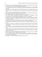
FIGURE 2.4 Modern flows in d esign automation.
That is, there is a sequence in which channels can be routed with fully specified longitudinal pin
positions. Switch boxes are not necessary. Moreover,channels are just rectangles between the slices,
with a shape constraint based on the information provided by the global router (almost all channels
can be routed close to density, and density can be estimated when there is a good idea of where the
pins of the nets are going to be).
Shapes only have to be assessed, and the assessment can be updated whenever more information
comes available. Once the cell assemblers (among which channel routers) are called, the shapes
become final. Floorplan optimization can then be called to convert the floorplan into a p lacement
with exact coordinates. Slicing floorplans can be optimized quickly. Therefore, there is no harm in
calling it whenever convenient. Thus, iteration-free synthesis was enabled. Figure 2.4 shows in the
black boxes a generic iteration-free flow. The essence is that each block makes its decisions once
and the flow never goes back to it. In the reality of the 1980s, slicing guaranteed wiring when used
in a (possibly hierarchical) floorplanning context. With more wiring layers available, the premise of
this solution was no longer valid.
2.4.2 TIMING CLOSURE
The first reaction to demands concerning speed were to include timing analysis in the tool set. After
producing the geometry of the layout, the netlist got extended with parasitics and other network
elements to determine its performance. The dynamical tuning of net weights was never a good idea
because of convergence problems. Soon wire-load models were developed to obtain more precise
estimates and indications where the critical paths were. Transistor sizing, buffer insertion, and fanout
tree construction could then improve timing without changing the logic. It did not take long before
logic resynthesis entered the scene, using these load models to make another netlist with hopefully
better timing properties. In Figure2.4, this is indicated by the dashed boxes and arrows.
All these measures in troduced iteration, the latter even global iteration over almost the complete
trajectory. And still it could only produce just another local optimum, notlikely to be global. In other
words, if timing demands were not met, one was never sure whether that was because the technology
of the day could not provide it or the tool set simply did not find it. With Moore’s law of unforgiving
push behind the chip market, this was not satisfactory.
A paradigm shift was needed and was found by adopting a delay model for gates that had roots
in a paper by Ivan E. Sutherland and Robert F. Sproull [59], and was justified in practice by Joel
Alpert/Handbook of Algorithms for Physical Design Automation AU7242_C002 Finals Page 24 24-9-2008 #17
24 Handbook of Algorithms for Physical Design Automation
Grodstein, Eric Lehman, Heather Harkness, William J. Grundmann, and Yoshinori Watanabe [60].
The key observation was that the size of a gate with constant delay varies linear ly with the load.
Writing this down for a network (not necessarily acyclic) leads to solving a set of linear equations for
gate sizes (a so-called Leontieff system), which can be iteratively updated with the sizes to adjust the
capacitive loads, and will surely converge if there are no limitations on the gate sizes [61]. Timing
could be guaranteed (if feasible) for networks that could be modeled with lumped capacitances,
which was true for all networks within the scope of the logic synthesis tools in those days.
With timing no longerthe moreorless arbitraryoutcome ofan optimizationwith area/wirelength
as its objective, the uncertainty shifted to area. Buffer insertion kept a spot in the flow, but now no
longer for improving speed. Buffers can only slow down a path in a network sized by the Leontieff
method. Timing can only be kept within the specification when buffers are inserted in noncritical
paths with enoughslack. That might be beneficial, because it may save area, but it would n ever make
the network faster. In addition, the flow became iteration free again as can be seen in Figure2.4 with
only the black and grey boxes included.
2.4.3 WIRE PLANNING
The complexity ofchips in the meantimehad developedfrom astate in which delaywas mainlycaused
by capacitive loads, predominantly gate capacitances, to a situation where most of the global delay
was in the wires. Whereas the Sutherland model maintains it salient property as long as resistance
between the gate and its load could be neglected, it was of little value when performance critically
depends on the distributed resistance and capacitance of wires on today’s chips. A delay model
published shortly after the Second World War [62], named Elmore delay after the author, was the
basis of much of the research on performance of de signs in silicon in the second half of the decade
of the 1990s. It was pretty accurate for point-to-point connections when it predicted that the delay
of long wires depended quadratically on their lengths. It could also be used in combination with the
buffer models of Takayasu Sakurai [63] to show that when optimally segmented, the delay became
linear in its length (regardless of the size of these buffers). The length of these segments did depend
on the layer (or rather o n the resistance and capacitance per unit length). An interesting observation
however is that the delay of a segment in an optimally segmented and buffered wire (of course also
an optimum size can be determined for the buffers) does not depend on the layer: it depends on the
properties of the transistors in the buffer. This implies that the delay is known as soon as the process
is chosen in which the buffers are going to be made [61].
These theoretical facts ope n new possibilities for design automation of the b ackend, and a wealth
of opportunitiesfor research. A lot of assumptions are quite idealistic: there is not always place for a
buffer at its optimal position, derivations are usually for homogeneous wires, connections are trees
in general, etc. But the two observations of delay in length and segment delay independent of layer
enable a scenario for wire planning:
1. Assign global wires as connection between modules that synthesis can cope with and
therefore so small that buffering does not help in speedup.
2. For given chip performance do time budgeting with convex time-size trade-offs for the
modules.
3. Synthesize netlists for the modules with function and delay for all gates.
4. Size the gates for constant delay.
In Figure 2.4, the scenario is depicted (exclude the dashed boxes and arrows) and shows that
no global iterations are implied. An initial footprint has to be chosen though, and convex trade-offs
(enabling efficient area minimization under timing bounds) have to be available (or extracted). Only
after time budgeting is it clear whether the design will fit in the chosen floorplan. Timing closure for
large chips is not yet fully solved.
Alpert/Handbook of Algorithms for Physical Design Automation AU7242_C002 Finals Page 25 24-9-2008 #18
Layout Synthesis: A Retrospective 25
2.5 WHAT DID WE LEARN?
The present goal of design automation has to be design closure, that is, how to specify a function to
be implemented on a chip, feed it to an electronic design automation (EDA) tool, and get, without
further interaction, a design that meets all requirements concerning functionality, speed, size, power,
yield, and other costs. It is the obvious quest of industry and the natural evolution from the sequence
of closure problems of the past decennium. Instead of focusing on trade-offs between two or three
performance characteristics whenever such a closure p roblem surfaces such as how to achieve wire-
ability in placement of components o r modules on a chip, how to allocate resources to optimize
schedules, or how to ensure timing convergence with minimal size, a more general approach should
be taken that in principle accounts for all combinations of performance characteristics [64].
No doubt the best algorithms developed in layout synthesis in the last 15 years will be key
ingredients and will get due attention in this book. Today’s practice of offering rigorous background
and thorough evaluation, preferably using well-established benchmarks, will be exemplified.
REFERENCES
1. C.Y. Lee, An algorithm for path connections and its applications, IRE Transactions on Electronic
Computers, EC-10(3): 346–365, September 1961.
2. E.W. Dijkstra, A note on two problems in connexion with graphs, Numerische Mathematik, 1: 269–271,
1959.
3. E.F. Moore, Shortest path through a maze, Annals of the Computation Laboratory of Harvard University,
30: 285–292, 1959.
4. S.B. Akers, A modification of Lee’s path connection algorithm, IEEE Transactions on Electronic
Computers, EC-16(1): 97–98, February 1967.
5. D.W. Hightower, A solution to line-routing problems on the continuous plane, in Proceedings of the 6th
Design Automation Workshop, Las Vegas, NV, pp. 1–24, 1969.
6. K. Mikami and K. Kabuchi, A computer program for optimal routing of printed circuit connectors, IFIPS
Pr oceedings, H47: 1475–1478, 1968.
7. W. Heyns, W. Sansen, and H. Beke, A line-expansion algorithm for the general routing p roblem with
a guaranteed solution, in Proceedings of the 17th Design Automation Conference, M inneapolis, MN,
pp. 243–249, 1980.
8. T. Asano, M. Sato, and T. Ohtsuki, Computational geometry algorithms, Chapter 9, in Layout Design and
Verification, ed. T. Ohtsuki, North-Holland, Amsterdam, the Netherlands, pp. 295–347, 1986.
9. F. Rubin, The lee path connection algorithm, IEEE T ransactions on Computers, C-23(9): 907–914,
September 1974.
10. P.E. Hart, N.J. Nilsson, and B. Raphael, A formal basis for the heuristic determination of minimum cost
paths, IEEE Tr ansactions on Systems Science and Cybernetics, SSC4(2): 100–107, 1968.
11. J. Munkres, Algorithms for t he assignment and transportation problems, Journal of the Society of I ndustrial
and Applied Mathematics, 5(1): 32–38, March 1957.
12. P.C. Gilmore, Optimal and suboptimal algorithms for the quadratic assignment problem, Journal of the
Society of Industrial and Applied Mathematics, 10(2): 305–313, June 1962.
13. L. Steinberg, The backboard wiring problem: A placement algorithm, Society of Industrial and Applied
Mathematics Reviews, 3(1): 37–50, January 1961.
14. C.J. Fisk, D.L. C askey, and L.L. West, ACCEL: Automated circuit car d etching layout, Proceedings of the
IEEE, 55(11): 1971–1982, November 1967.
15. M. Hanan and J.M. Kurtzberg, A review of the placement and quadratic assignment problems, Society of
Industrial and Applied Mathematics Reviews, 14(2): 324–342, April 1972.
16. K.M. Hall, An r-dimensional quadratic placement algorithm, Management Science, 17(3): 219–229,
November 1970.
17. M.C. van Lier and R.H.J.M. Otten, Automatic IC layout: The model and technology, IEEE Transactions
on Circuits and Systems, 22(11): 845–855, November 1975.
18. R.H.J.M. Otten and J.G. van Wijk, Graph representations in interactive layout design, in Proceedings IEEE
International Symposium Circuits and Systems, New York, NY, pp. 914–918, 1978.
Alpert/Handbook of Algorithms for Physical Design Automation AU7242_C002 Finals Page 26 24-9-2008 #19
26 Handbook of Algorithms for Physical Design Automation
19. T. Ohtsuki, N. Sugiyama, and H. Kawanishi, An optimization technique for integrated circuit layout design,
in Proceedings of the ICCST-Kyoto, Kyoto, Japan, pp. 67–68, September 1970.
20. R.L. Brooks, C.A.B. Smith, A.H. Stone, and W.T. Tutte, The dissection of rectangles into squares, Duke
Mathematical Journal, 7: 312–340, 1940.
21. A.S. Lapaugh, Algorithms for integrated circuit layout, PhD thesis, MIT, Boston, MA, November 1980.
22. A. Hashimoto and J. Stevens, Wire routing by optimizing channel assignment within large apertures, in
Pr oceedings of the 8th Design Automation Workshop, Atlantic City, NJ, pp. 155–169, 1971.
23. P.R. Groeneveld, Necessary and sufficient conditions for the routability of classical channels, Integration,
the VLSI Journal, 16: 59–74, 1993.
24. T.G. Szymanski, Dogleg channel routing is NP-complete, IEEE T ransactions on CAD of Integrated Circuits
and Systems, 4(1): 31–41, January 1985.
25. P.R. Groeneveld, H. Cai, and P. Dewilde, A contour-based variable-width gridless channel router, in
Pr oceedings of the International Conference on Computer-Aided Design, San José, CA, pp. 374–377,
1987.
26. U.R. Kodres, Geometrical positioning of circuit elements in a computer, in AIEE Fall General Meeting,
Chicago, ILL, No. 59-1172, October 1959.
27. U.R. Kodres, Partitioning and card selection, Chapter 4, in Design Automation of Digital Systems,Vol.1,
ed. M.A. Breuer, Prentice Hall, Engle wood Cliffs, NJ, pp. 173–212, 1972.
28. B.W. Kernighan and S. Lin, An efficient heuristic procedure for partitioning graphs, Bell System Technical
Journal, 49(2): 291–307, February 1970.
29. C.M. Fiduccia and R.M. Mattheyses, A linear time heuristic for improving network partitions, in
Pr oceedings of the 19th Design Automation Conference, Las Vegas, NV, pp. 175–181, 1982.
30. W.E. Donath and A.J. Hoffman, Algorithms for partitioning of graphs and computer logic based on
eigenvectors of connection matrices, IBM Technical Disclosure Bulletin, 15: 938–944, 1972.
31. M.A. Breuer, A class of min-cut placement algorithms, i n Proceedings of the 14th Design Automation
Conference, New Orleans, LA, pp. 284–290, 1977.
32. U. Lauther, A min-cut placement algorithm for general cell assemblies based on a graph representation, in
Pr oceedings of the 16th Design Automation Conference, San D ie go, CA, pp. 1–10, 1979.
33. A.E. Dunlop and B.W. Kernighan, A procedure for placement of standard-cell VLSI circuit, IEEE
Transactions on CAD of Integrated Circuits and Systems, CAD-4 (1): 92–98, January 1985.
34. S. Goto, An efficient algorithm for the two-dimensional placement problem in electrical circuit layout,
IEEE Transactions on Circuits and Systems, CAS-28 (1): 12–18, January 1981.
35. B.T. Preas and C.W. Gwyn, Methods for hierarchical automatic layout of custom LSI circuit masks, in
Pr oceedings of the 15th Design Automation Conference, pp. 206–212, 1978.
36. C. Mead and L . Conway, Introduction to VLSI Systems, Addison-Wesley, Reading, MA, 1980.
37. R.H.J.M. Otten, Automatic floorplan design, in Proceedings of the 19th Design Automation Conference,
Las Vegas, NV, pp. 261–267, 1982.
38. S.B. A kers, J.M. Geyer, and D.L. Roberts, IC mask layout with a single conductor layer, in Proceedings of
the 7th Workshop on Design Automation, San F rancisco, CA, pp. 7–16, 1970.
39. H. Murata, F. Fujiyoshi, S. Nakatake, and Y. Kajitani, VLSI module placement based on rectangle packing
by the sequence-pair, I EEE Transactions on Computer-Aided Design, 15: 1518–1524, December 1996.
(ICCAD 1995).
40. J. Grason, A dual linear graph representation for space-filling location problems of the floor plan type,
in Emerging Methods in En vironmental Design and Planning, ed. G.T. Moore, Proceedings of the Design
Methods Group, 1st International Conference, Cambridge, MA, pp. 170–178, 1968.
41. J. Bhasker and S. Sahni, A l inear algorithm to find a rectangular dual of a planar triangulated graph,
Algorithmica, 3: 247–278, 1988.
42. C.T. McMullen and R.H.J.M. Otten, Minimum length linear transistor arrays in MOS, in IEEE International
Symposium on Circuits and Syst ems, Kyoto, Japan, pp. 1783–1786, 1988.
43. R.L. Maziasz and J. P. Hayes, Layout Minimization of CMOS Cells, Kluwer Academic Publishers, Boston,
MA; Dordrecht, The Netherlands; London, U.K., 1992.
44. M. Sarrafzadeh and C K. Wong, An Introduction to VLSI Physical Design, McGraw-Hill Companies Inc.,
Hightstown, NJ, 1996.
45. S.M. Sait and H. Youssef,
VLSI Physical Design Automation,
M
cGraw-Hill Companies Inc./IEEE Press,
Hightstown, NJ, 1995.
Alpert/Handbook of Algorithms for Physical Design Automation AU7242_C002 Finals Page 27 24-9-2008 #20
Layout Synthesis: A Retrospective 27
46. N. Sherwani, Algorithms for VLSI Physical Design Automation, Kluwer Academic Publishers, Boston, MA;
Dordrecht, The Netherlands; London, U.K., 1995.
47. T. Lengauer, Combinatorial Algorithms for Integrated Circuit Layout, John Wiley & Sons, N ew York;
Berlin, Germany, 1990.
48. L. Stockmeyer, Optimal orientations of cells in slicing floorplan designs, Information and Contr o l, 57(2–3):
91–101, May/June 1983.
49. R.H.J.M. Otten, Efficient floor plan optimization, in Pr oceedings of International Conference on C omputer
Design, Portchester, NY, pp. 499–503, October–November 1983.
50. T. Lengauer and R. Müller, The complexity of floorplanning based on binary circuit partitions, Techni-
cal Report 46, Department of Mathematics and Computer Science, University of Paderborn, Paderborn,
Germany, 1986.
51. L.P.P.P. van Ginneken and R.H.J.M. Otten, Optimal slicing of plane point placements, Proceedings of the
Conference on European Design Automation, Glascow, U.K., pp. 322–326, 1990.
52. S. Kirkpatrick, C.D. Gelatt, and M.P. Vecchi, Optimization by simulated annealing, Science, 220(4598):
671–680, 1983.
53. V. Cerny, A thermodynamical approach to the travelling salesman problem: An efficient simulation
algorithm, Journal of Optimization Theory and Applications, 45: 41–51, 1985.
54. N. Metropolis, A.W. Rosenbluth, M.N. Rosenbluth, A.H. Teller, andE. Teller, Equations of state calculations
by fast computing machines, Journal of Chemical Physics, 21(6): 1087–1092, 1953.
55. R.H.J.M. Otten and L.P.P.P.van Ginneken, The Annealing Algorithm, Kluwer Academic Publishers, Boston,
MA; Dordrecht, The Netherlands; London, U.K., 1989.
56. S.A. Solla, G.B. Sorkin, and S.R. White, Configuration space analysis for optimization problems, in Dis-
ordered Systems and Biological Organization, eds. E. Bienenstock et al., NATO ASI Series, F20, S pringer
Verlag, Berlin, Germany, pp. 283–293, 1986.
57. C. Sechen and A.L. Sangiovanni-Vincentelli, The timberwolf placement and routing package, IEEE Journal
of Solid-State Circuits, 20: 510–522, 1985.
58. D.F. Wong and C.L. Liu, A new algorithm for floorplan design, in Proceedings of the 23rd Design
Automation Conference, Las Vegas, NV, pp. 101–107, 1986.
59. I.E. Sutherland and R.F. Sproull, Logical effort: Designing for speed on the back of an envelope, in Pro-
ceedings of the 1991 University of California Santa Cruz Conference on Advanced Research in VLSI,
ed. C. Sequin, MIT Press, Santa Cruz, CA, pp. 1–16, 1991.
60. J. G rodstein, E. Lehman, H. Harkness, W.J. Grundmann, and Y. Watanabe, A delay model for logic synthesis
of continuously-sized networks, in Proceedings of the International Conference on Computer-Aided Design,
San Francisco, CA, pp. 458–462, 1995.
61. R.H.J.M. Otten, A design flo w for performance planning: New paradigms for i teration free synthesis,
in Architecture Design and Validation Methods, ed. E. Böerger, Springer, Berlin, Heidelberg, Germany;
New York, pp. 89–139, 2000.
62. W.C. Elmore, The transient analysis of damped linear networks with particular regard to wideband
amplifiers, Journal of Applied Physics, 19(1): 55–63, January 1948.
63. T. Sakurai, Approximation of wiring delay in MOSFET LSI, IEEE J ournal of Solid-State Circuits, 18(4):
418–426, August 1983.
64. M.C.W. Geilen, T. Basten, B.D. Theelen, and R.H.J.M. Otten, An algebra of Pareto points, Fundamenta
Informaticae, 78(1): 35–74, 2007.
Alpert/Handbook of Algorithms for Physical Design Automation AU7242_C002 Finals Page 28 24-9-2008 #21
Alpert/Handbook of Algorithms for Physical Design Automation AU7242_C003 Finals Page 29 29-9-2008 #2
3
MetricsUsedinPhysical
Design
Frank Liu and Sachin S. Sapatnekar
CONTENTS
3.1 Timing 29
3.1.1 Elmore Delay and Slew Metrics 30
3.1.1.1 Elmore Delay 30
3.1.1.2 Elmore Delay for RC Trees 32
3.1.1.3 Elmore Delay for Nontrees 33
3.1.1.4 Elmore Slew 34
3.1.1.5 Limitations of Elmore Delay 35
3.1.2 Fast Timing Metrics 35
3.1.2.1 PRIMO and H-Gamma 35
3.1.2.2 Weibull-Based Delay 36
3.1.2.3 Lognormal Delay 38
3.1.3 Fundamentals of Static Timing Analysis 39
3.2 Noise 42
3.3 Power 44
3.3.1 Dynamic Power 44
3.3.2 Short-Circuit Power 46
3.3.3 Static Power 46
3.4 Temperature 48
Acknowledgment 50
References 50
Physical design consists of a number of steps that attempt to optimize one or more specified
design objectives, under one or more design constraints. This optimization is based on predictors
and metrics that measure the value of the circuit property. These metrics must be computationally
efficient,so that they may beembedded in the innerloop of an optimizerand may be called repeatedly
during optimization, and yet have sufficient accuracy that is commensurate with the needs of the
specific stage of physical design. In this chapter, we overview several metrics that may be used
in objective and constraint functions in physical design, used to measure circuit properties such as
timing, noise, power, and temperature. It should be noted that although area is also a metric used in
optimization, area metrics are generally quite simple, and are not covered in this chapter.
3.1 TIMING
For most of today’s VLSI d esigns, a dominant portion is synchronous in nature. In a synchronous
design, a main clock signal is required to coordinate the operation of various logic blocks across
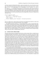
the chip. A highly simplified view of a logic block is shown in Figure 3.1. The block consists of a
cluster of combinationalcircuits, surrounded by the input and output latch banks, which may, e.g., be
29
Alpert/Handbook of Algorithms for Physical Design Automation AU7242_C003 Finals Page 30 29-9-2008 #3
30 Handbook of Algorithms for Physical Design Automation
Latch bank A Latch bank B
Combinational
elements
Clock
FIGURE 3.1 An illustrative timing diagram of a sequential circuit.
level clocked or edge triggered. A clock signal synchronizes the operations of the latch banks. The
input latch bank provides primary inputs, which are computational results of the previous stage, to
the combinational cluster, and the results of the logic computation are stored (or latched) by the
output latch bank. Because the two latch banks open at a fixed interval, which is determined by the
frequencyof the clock signal, the time the combinational cluster takes to complete logic computation
has to meet this constraint. In a modern VLSI design, the circumstance is much more complicated,
but the general principle still holds.
It is quite likely that the combinational cluster will be constructed by the instances of logic gates
from a predefined library. The timing perfor mance of the combinational block is a strong function
of the physical design, such as the placement of the gates, the routing of signal wires, as well as the
sizing of the transistors. Therefore, any of these physical design optimizations must be guided by
fast timing evaluators.
In thischapter, webriefly introducethetiming metricscommonly usedin physicaldesign.Wefirst
review the classic Elmore delay and slew metric, followed by more advanced fast timing estimation
metrics. Finally, we review the fundamentals of static timing analysis of combinational circuits.
3.1.1 ELMORE DELAY AND SLEW METRICS
The dynamic behavior o f an interconnect structure can be described by a system of ordinary differ-
ential equations. From a physical design point of view, this behavior can be characterized by two
quantities: d elay and slew (or rise/fall time), as depicted in Fig ure 3.2. This section outlines tech-
niques for calculating these two quantities efficiently, with the given parameters of the interconnect
structure.
3.1.1.1 Elmore Delay
The Elmore delay was first proposed by W. C. Elmore in 1948 [1], but did not receive much attention
for over three decades. It was not until the 1980s, when the wire delays on an integrated circuit
became nonnegligible, that it was rediscovered by Rubenstein et al. [2], and today, it is still the
most popular timing metric in physical optimization. The reason for its popularity can be attributed
not only to its simplicity but also to other important characteristics such as additivity, which we
discuss later.
We will proceed under the reasonable assumption that an interconnect structure can be modeled
as a set of lumped RLC segments, and we represent the impulse response of a specific node voltage
in the circuit by h(t). If we denote the Laplace transformation of h(t) as H(s), we can expand it into
a Taylor series at s = 0:
Alpert/Handbook of Algorithms for Physical Design Automation AU7242_C003 Finals Page 31 29-9-2008 #4
Metrics Used in Physical Design 31
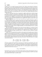
Slew
Delay
t
V
FIGURE 3.2 Delay and slew of a wire segment.
H(s) =
∞
0
h(t) e
−st
dt =
∞
k=0
(−1)
k
k!
s
k
∞
0
t
k
h(t)dt (3.1)
Therefore,
H(s) = m
0
+ m
1
s +m
2
s
2
+ m
3
s
3
+··· (3.2)
where
m
k
=
(−1)
k
k!
∞
0
t
k
h(t)dt for k = 0, 1, 2, (3.3)
The coefficients of the Taylor expansion is commonly known as the (circuit) moments.
Foran RCcircuit withoutresistivepath toground,the impulseresponse h(t) satisfiesthe following
conditions:
⎧
⎨
⎩
h(t) ≥ 0, ∀ t
∞
0
h(t)dt = 1
(3.4)
In probability theory, any continuous real function that satisfies Equation3.4 is a probability
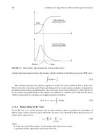
density function (PDF). The integral of a PDF is defined as a cumulative density function:
S(t) =
t
0
h(τ )dτ (3.5)
This corresponds to the step response in circuit analysis (Figure3.3).
Several characteristics are commonly used to d escribe a statistical distribution. The first is the
mean, which is defined as
µ =
∞
0
th(t)dt (3.6)