- Trang chủ >>
- Khoa Học Tự Nhiên >>
- Vật lý
Handbook of algorithms for physical design automation part 6 pot
Bạn đang xem bản rút gọn của tài liệu. Xem và tải ngay bản đầy đủ của tài liệu tại đây (190.55 KB, 10 trang )
Alpert/Handbook of Algorithms for Physical Design Automation AU7242_C003 Finals Page 32 29-9-2008 #5
32 Handbook of Algorithms for Physical Design Automation
Step response
interpreted as CDF
Impulse response
interpreted as PDF
Mean
t
t
Delay
Median
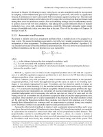
FIGURE 3.3 Elmore delay: approximating the median with the mean.
Another important characteristic is the median, which is defined as the halfway point on a PDF curve:
M
0
h(t)dt =
1
2
(3.7)
The similarity between the impulse response of an RC tree and a statistical PDF is quite clear.
Observe that the commonly used 50 percent delay point in circuit analysis actually corresponds to
the median of the underlying distribution. This is the keen observation of Elmore in 1948. Moreover,
he also made the proposal that as the median was difficult to calculate, one could use the mean,
which is much easier to calculate, as an approximation of median:
M ≈ µ =−m
1
=
∞
0
th(t)dt (3.8)
3.1.1.2 Elmore Delay for RC Trees
For an RC tree (i.e., an RC network with no direct resistive path to ground), the calculation of
Elmore delay can be carried out quite efficiently. In such a case, the Elmore delay between any two
nodes can be expressed as
µ =
R
i
·
downstream
C
j
(3.9)
where
R
i
is the traversal of the resistors on the unique path between two nodes
C
j
permutes all the capacitance seen from resistor R
i
Alpert/Handbook of Algorithms for Physical Design Automation AU7242_C003 Finals Page 33 29-9-2008 #6
Metrics Used in Physical Design 33
R
1
R
3
R
4
R
5
R
6
C
5
C
4
C
3
C
6
C
2
C
1
R
2
A
Z
1
Y
E
2
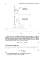
FIGURE 3.4 An example of RC tree to illustrate the process of calculating Elmore delay.
For the simple example shown in Figure3.4, the Elmore delay from root node A and fan-out
node Z1 can be calculated by traversing the unique resistive path from Z1toA:
ED
A→Z1
= R
5
C
5
+ R
4
(C
4
+ C
5
) + R
3
(C
3
+ C
4
+ C
5
)
+ R
2
(C
2
+ C
3
+ C
4
+ C
5
+ C
6
)
+ R
1
(C
1
+ C
2
+ C
3
+ C
4
+ C
5
+ C
6
)
The Elmore delay has a nice property: it is additive. In other words, for two nodes A and C on a
branch, if node B lies between A and C, we can write:
ED
A→C
= ED
A→B
+ ED
B→C
For the example shown in Figure 3.4, we can easily verify that
ED
A→Y
= R
3
(C
3
+ C
4
+ C
5
) + R
2
(C
2
+ C
3
+ C
4
+ C
5
+ C
6
)
+ R
1
(C
1
+ C
2
+ C
3
+ C
4
+ C
5
+ C
6
)
ED
Y→Z1
= R
5
C
5
+ R
4
(C
4
+ C
5
)
Thus,
ED
A→Z1
= ED
A→Y
+ ED
Y→Z1
The Elmore delay of an RC tree has another important property: it can be proven to be the upper
bound of the true 50 percent circuit delay under anyinput excitation [3]. In other words, if a particular
RC net is optimized based on the Elmore delay,its real delay is guaranteed to be better. Empirically it
has been shown that although the Elmore delay is the upper bound, the error can be quite substantial
in some cases, especially for those nodes close to the driving point. The accuracy for far-end nodes
(those close to the sink pins) is much better. Note that this property only applies to RC trees, and it
does not hold for nontree circuits, e.g., meshes.
The Elmore delay can also be calculated for distributed circuits. For a uniform wire at the length
of L, with a unit resistance R, a unit capacitance C, and a loading capacitance C
L
, it can be shown
that the Elmore delay at the far-end of the wire is
ED =
1
2
RL(CL + C
L
)
3.1.1.3 Elmore Delay for Nontrees
For a nontree RC network, the calculation of Elmore delay is more involved. The simple traversal
algorithm for tree-like structures is no longer valid. Instead, we can formulate the circuit into the
Alpert/Handbook of Algorithms for Physical Design Automation AU7242_C003 Finals Page 34 29-9-2008 #7
34 Handbook of Algorithms for Physical Design Automation
modified nodal analysis (MNA) formulation and solve for the moments. In this case, a linear circuit
can be formulated as
Gx(t) + C
d
dt
x(t) = Bu(t)
where
G is the conductance matrix
C is the capacitance matrix
matrix B specifies where the excitations are applied
The entries in unknown vector x(t) consists of node voltages, branch currents of voltage sources,
as well as branch currents of inductors. u(t) is the external time-varying excitation. The L aplace
transformation of the MNA formulation is
GX(s) +sCX(s) = BU(s)
The first circuit m oment is
m
1
=−G
−1
CG
−1
B
Therefore, the Elmore delay at a particular node can be calculated by selecting the corresponding
entry in the vector of the first moment:
ED
i
= e
T
i
G
−1
CG
−1
B
where vector e
i
is the selection vector with all entries zero except at the ith location.
Computationally,only one LU factorization of the conductance matrix G is required in the above
calculation, an d the rest of calculation is merely forward–backward substitution of the prefactorized
matrix as well as matrix–vector multiplication, which can be carried out quite efficiently.
It is also worth pointing out that the above procedure is the general description of the Elmore
delay calculation for any linear circuit. Thus, it can be used to calculate the Elmore delay of an RC
tree as well. However, due to its special topology, the LU factorization o f an RC tree can be carried
out without explicit formulation of the conductance and capacitance matrices, and a closed-form
formula, described earlier, for the Elmore delay can be obtained. More details on how to construct
the MNA matrices and the calculation of Elmore delay for a general circuit can be found in Ref. [4].
3.1.1.4 Elmore Slew
In his original paper, Elmore refereed to slew as the gyration. If we follow the probability interpre-
tation of signal transition, it can be shown that just as the delay corresponds to the median of the
PDF function, the slew corresponds to the variance of the PDF function. A first-order estimate of
variance is the second central moment, which is defined as
σ
2
= m
2
1
− 2m
2
In practice, because quite often slew is defined as the difference of delay between 10 percent and
90 percent delay points, the above metric needs to be scaled accordingly.
Slew =
8
10
m
2
1
− 2m
2
Note that we need the second circuit moment to calculate the slew. In gen eral, it can be shown that
the second circuit moment can be calculated in MNA formulation as
m
2
= G
−1
CG
−1
CG
−1
B
In practice, the factorized matrix G during m
1
calculation can be reused to calculate m
2
.
Therefore, the added computationa l complexity is only a few matrix–vector m ultiplications and
Alpert/Handbook of Algorithms for Physical Design Automation AU7242_C003 Finals Page 35 29-9-2008 #8
Metrics Used in Physical Design 35
backward/forwardsubstitutions, which are usually much cheaper than matrix factorizatio n itself. For
RC trees, the matrix does not need to be explicitly formulated and factorized at all. The path-tracin g
algorithm used in m
1
calculation can be applied as well. More details can be found in Ref. [4].
3.1.1.5 Limitations of Elmore Delay
As we have discussed earlier, the Elmore delay has a few very nice properties when applied on RC
trees. They are
• Easy to calculate
• Proven to be the upper bound for any node under any input excitation
• Additive along the signal path
During physical design, most on-chip signal wires can be modeled as trees, therefore, the Elmore
delay has been quite popular and has been implemented in many physical design algorithms.
However, the Elmore metric also has some limitations, especially in terms of accuracy. Empiri-
cally it has been shown that even for RC trees, the accuracy of Elmore delay can be over ten times
off at certain nodes, especially for the nodes close to the driving point. The reason for this inaccuracy
can be explained as follows: the essence of Elmore delay is to use mean to approximate median for
a particular PDF. Such an approximation is only accurate when the PDF is unimodal and has zero
skew, e.g., the PDF is symmetric. For an RC tree, this is only true for far-end nodes. For the near-end
nodes (the ones which are close to the driving point), the skewness of the impulse response (which
we interpreted as a PDF) is quite large. As a consequence, the approximation used in Elmore delay
becomes inaccurate.
3.1.2 FAST TIMING METRICS
The essence of Elmore delay is the probability interpretation of the impulse response of a linear
circuit. This allows the signal response to b e approximated by using a structured continuous function
as the template, thus making it possible to quickly extract delay and slew metrics. In the derivation of
Elmore delay, it is assumed that the underlying PDF function is symmetric. A natural extension of the
idea is to remove this assumption: we can use an asymmetric PDF and hopefully the accuracy can be
improved. In the first proposed method [5], the gamma distribution function was used as the template
function. Later on, other distribution functions are proposed to be the template function, including
the Weibull [6] and lognormal [7] functions. Another benefit of these extended approaches is that we
are no longer limited to the 50 percent delay point. Once the parameters of the function template are
known, we can calculate any percentile de lay po int. The price we have to pay to get better accuracy is
thatmoremoments areneeded.Besides,allofthese fastdelay metricscannotbe provedto be theupper
bound of the true delay, although empirically it has been shown that overall they are more accurate.
3.1.2.1 PRIMO and H-Gamma
The idea of PRIMO [5] was to approximate the circuit impulse response as the PDF function of a
gamma distribution. Because only two parameters are needed to determine a gamma distribution,
these two parameters can be easily determined by applying the moment-matching principle. Once
the coefficients of the gamma distribution are known, we do not need to approximate the median
with the mean. Instead, we can directly calculate the median, which corresponds to the 50 percent
delay. Later, an improved version of gamma fitting was introduced in H-gamma [8]. Here, we only
describe H-gamma.
The gamma statistical distribution is defined on support x > 0, with the PDF defined as
f (x; k, θ) =
θ
k
x
k−1
e
−θx
(k)
Alpert/Handbook of Algorithms for Physical Design Automation AU7242_C003 Finals Page 36 29-9-2008 #9
36 Handbook of Algorithms for Physical Design Automation
where (k) is the gamma function:
(k) =
∞
0
x
k−1
e
−x
dx
Each gamma distribution is uniquely determined by two parameters, k and θ , and both of them have
to be positive. The mean and the variance of a gamma distribution are
mean =
k
θ
variance =
k
θ
2
To derive H-gamma, we can rewrite the impulse response of a circuit node as
Y(s) = m
0
+ m
1
s +m
2
s
2
+ m
3
s
3
+···
= m
0
+ m
1
s
1 +
m
2
m
1
s +
m
3
m
1
s
2
+···
The series in parenthesis is referred as the normalized homogeneous function. In H-gamma, the
normalized homogeneous function is fit into the PDF of a gamma distribution by matching the first
two moments. The results are
k
θ
=−
m
2
m
1
k
θ
2
= 2
m
3
m
1
−
m
2
m
1
2
Once two parameters k and θ are calculated, we can approximate the step response as
y(t) ≈ 1 + m
1
θ
k
t
k−1
e
−θt
(k)
The delay at any percentile point φ can be calculate by setting the left-hand-side of the above
equation to φ and solve for t. Unfortunately, this process requires a nonlinear iteration method such
as Newton–Raphson because this equation cannot be explicitly solved.
To address thisissue, thenonlinear iteration process canbesimplified to atablelook-upprocedure
by scaling time t with θ,andk with −m
1
. The scaled response approximation can be shown to be
y
λ,k
(x) = 1 −
λx
k−1
e
−x
(k)
For any percentile φ, a two-dimensionaltable needs to b e preconstructed with λ and k as the input and
x as the output. The final delay is then calculated b y scaling x with θ: t = x/θ . Empirically it has been
shown that H-gamma metric has good accuracy for both near and far-end nodes. One reason for its
accuracyis particularly due to the fact that three moments are used to calculate the delay at each node.
3.1.2.2 Weibull-Based Delay
Another proposed delay metric uses Weibull distribution as the underlying function template. The
advantage of using the Weibull distribution is that the percentile points are very easy to calculate.
A Weibull distribution is defined on the support of t > 0 and is determined by two parameters:
f (x : α, β) = αβ
−α
x
α−1
e
−(x/β)
α
Alpert/Handbook of Algorithms for Physical Design Automation AU7242_C003 Finals Page 37 29-9-2008 #10
Metrics Used in Physical Design 37
Both parameters, α and β, must be positive. Th e mean and variance of a Weibull distribution is
Mean = β(1 +θ)
Variance = β
2
[(1 +2θ) −
2
(1 +θ)]
Unlike the gammadistribution, in whichthe distribution parameterscanbeeasily calculated from
moments, the Weibull distribution requires iterative evaluation of gamma functions. To simplify the
process, it is proposed that a look-up table be precharacterized. The look-up table requires the first
two circuit moments as inputs and it returns the parameter θ:
r Log
10
(r) θ
0.63096 −0.2 0.48837
0.79433 −0.1 0.76029
1.00000 +0.0 1.00000
1.25892 +0.1 1.22371
1.58489 +0.2 1.43757
1.99526 +0.3 1.64467
2.51189 +0.4 1.84678
3.16228 +0.5 2.04507
3.98107 +0.6 2.24031
5.01187 +0.7 2.43305
6.30957 +0.8 2.62371
7.94328 +0.9 2.81262
10.00000 +1.0 3.00000
12.58925 +1.1 3.18607
15.84893 +1.2 3.37098
where r = m
2
/m
2
1
. Note that it is recommended to use log
10
(r) value in the interpolation. Once θ is
known, the other parameter, β, is calculated by using the following equation:
β =
−m
1
(1 +θ)
Although an evaluation of the gamma function is again needed, the following table can be used to
avoid the evaluation:
x Gamma(x )
1.0 1.00000
1.1 0.95135
1.2 0.91817
1.3 0.89747
1.4 0.88726
1.5 0.88623
1.6 0.89352
1.7 0.90864
1.8 0.93138
1.9 0.96176
2.0 1.00000
Alpert/Handbook of Algorithms for Physical Design Automation AU7242_C003 Finals Page 38 29-9-2008 #11
38 Handbook of Algorithms for Physical Design Automation
The table only covers the data range between 1 and 2, and the following recursive property of the
gamma function can be used to calculate other x:
(x + 1) = x(x) ∀ x > 1
Once α and β are known, the delay at any percentile φ can be calculated as
t
φ
= β
ln
1
1 −φ
θ
In particular, the 50 percent delay point can be calculated as
t
0.5
= β[ln(2)]
θ
≈ β · (0.693)
θ
3.1.2.3 Lognormal Delay
Another delay metric uses lognormal distribution for probability interpretation of responsesignal [7].
The lognormal distribution is determined by two parameters µ and σ. Its PDF is defined as
f (x; µ, σ) =
1
xσ
√
2π
exp
[ln(x) −µ]
2
2σ
2
Similar to Weibull-based delay, the first two circuit moments are matched to the moments of the
distribution to calculate µ and σ . Once they are known, the delay can be calculated by calculating
the median of the lognormal distribution. After simplification, it turns out that the 50 percent delay
metric is a closed form of the two circuit moments:
t
0.5
=
m
2
1
√
2m
2
The lognormal distribution can also be used to provide a closed-form slew metric. Because slew
metric is equivalent to the difference of two delay points (e.g., 10 p ercent and 90 percent delay), the
accuracy requirement is higher. In some cases, especially for the near-end nodes, metrics based on
two moments may not be sufficiently accurate. To achieve the balance between the accuracy and
complexity, a three-piece approach was proposed, based on the value of r = m
1
/
√
m
2
:
• r ≤ 0.35:
Slew
12
=
m
2
1
√
2m
2
e
kS
√
2
− e
−kS
√
2
where S =
ln(2m
2
/m
2
1
), and the value of k depends on the definition of slew and is
explained later.
• r ≥ 1
Slew
23
=
2m
2
− m
2
1
z(z − 1)
e
k
√
2ln(z)
− e
−k
√
2ln(z)
where z = (y−1/y)
2
+1andy =
3
(γ +
√
4 +γ
2
)/2, where γ = (−6m
3
+6m
1
m
2
−2m
3
1
)/
(2m
2
− m
2
1
)
3/2
and k is the function of slew ratio.
• 0.35 < r < 1
Slew =
20
13
r −
7
13
slew
23
+
20
13
(1 −r) slew
12
Alpert/Handbook of Algorithms for Physical Design Automation AU7242_C003 Finals Page 39 29-9-2008 #12
Metrics Used in Physical Design 39
The value k is the scaling factor needed to reflect difference in terms of slew definition. It is
calculated based on the table below:
Slew Definition k
10/90 0.9063
20/80 0.5951
25/75 0.4769
30/70 0.3708
3.1.3 FUNDAMENTALS OF STATIC TIMING ANALYSIS
As discussed earlier in this section, a sequential circuit consists of combinational elements and
sequential elements and can be represented as a set of combinational blocks that lie between latches.
This subsection presents methods that compute the delay of a combinational logic block.
A combinational logic circuit can be represented as a timing graph G = (V, E),wherethe
elements of V , the vertex set, are the logic gates in the circuit and the primary inputs and outputs
of the circuit. A pair of vertices, u and v ∈ G, are connected by a directed edge e(u, v) ∈ E if
there is a connection from the output of the element represented by vertex u to the input of the
element represented by vertex v. A simple logic circuit and its corresponding graph are illustrated
in Figure 3.5a and b, respectively. In this section, we present techniques that are used for the static
timing analysis of digital combinational cir cuits. The word “static” alludes to the fact that this timing
analysis is carried out in an input-independent manner, and purports to find the worst-case delay of
the circuit over all possible input combinations. The method is often referred to as CPM (critical
path method). The computational efficiency of CPM has resulted in its widespread use, even though
it has some limitations.
The CPM-based algorith m, applied to a timing graph G = (V, E), can be summarized by the
pseudocode shown below:
Algorithm CRITICAL_PATH_METHOD
Q =∅;
for all vertices i ∈ V
n_visited_inputs [i]= 0;
/∗ Add a vertex to the tail of Q if all inputs are ready ∗/
for all primary inputs i
/∗ Fanout gates of i ∗/
for all vertices j such that (i → j) ∈ E
if (++n_visited_inputs[j] == n_inputs[j]) addQ(j,Q);
while (Q =∅) {
g = top(Q);
remove
(
g,Q);
compute_delay[g]
/∗ Fanout gates of g ∗/
for all vertices k such that (g → k) ∈ E
if (++n_visited_inputs[k]== n_inputs[k]) addQ(k,Q);
}
The procedure is best illu strated by means of a simple examp le. Consider the circuit in Figure 3.6,
which sh ows an interconnection of blocks. Each of these blocks could be as simple as a logic gate
Alpert/Handbook of Algorithms for Physical Design Automation AU7242_C003 Finals Page 40 29-9-2008 #13
40 Handbook of Algorithms for Physical Design Automation
t
I1
I2
I4
I5
I3
O1
O2
G5
G6
G3
G4
G2
G1
s
(a) (b)
G6
G5
G1
G2
G3
G4
O1
O2
I4
I5
I3
I2
I1
FIGURE 3.5 (a) An example combinational circuit and (b) its timing graph. (From Sapatnekar, S. S., Timing,
Kluwer Academic Publisher , Boston, MA, 2004. With permission.)
or could be a more complex combinational block, and is characterized by the delay from each input
pin to each output pin. For simplicity, this example will assume that for each block, the delay from
any input to the output is identical. Moreover, we will assume that each block is an inverting logic
gate such as a NAND or a NOR, as shown by the “bubble” at the output. The two numbers, d
r
/d
f
,
inside each gate represent the delay corresponding to the delay of the output rising transition, d
r
,and
that of the output fall transition, d
f
, respectively. We assume that all primary inputs are available at
time zero, so that the numbers “0/0” against each primary input represent the worst-case rise and
fall arrival times, respectively, at each of these nodes. The critical path method proceeds from the
primary inputs to the primary outputs in topological order, computing the worst-case rise and fall
arrival times at each intermediate node, and eventually at the outputs of a circuit.
A block is said to be ready for processing when the signal arrival time information is avail-
able for all of its inputs; in other words, when the number of processed inputs of a gate g,
n_visited_inputs[g], equals the number of inputs of the gate, n_inputs[g]. Notation-
ally, we refer to each block b y the symbol for its output node. Initially, because the signal arrival
times are known only at the primary inputs, only those blocks that are fed solely by primary inputs are
ready for processing. In the example, these correspond to the gates i, j, k,andl. These are placed in a
queue Q using the function addQ, and are processed in the order in which they appear in the queue.
In the iterative pr ocess, the block at the head of the queue Q is taken off the queue and scheduled
for processing. Each processing step consists of
m
a
b
c
d
e
f
g
h
2/1
4/2
4/2
3/1
3/5
8/5
7/6
7/11
0/0
0/0
0/0
0/0
0/0
0/0
0/0
0/0
p
n
o
l
k
j
i
2/1
4/2
3/1
4/2
2/2
1/3
3/2
1/1
FIGURE 3.6 An example illustrating the application of the CPMon a circuit with inverting gates. The numbers
within the gates correspond to the rise delay/fall delay of the block, and the bold numbers at each block output
represent the rise/fall arrival times at that point. The primary inputs are assumed to have arrival times of zero,
as sho wn. (From Sapatnekar, S. S., Timing, Kluwer A cademic Publisher, Boston, MA, 2004. With permission.)
Alpert/Handbook of Algorithms for Physical Design Automation AU7242_C003 Finals Page 41 29-9-2008 #14
Metrics Used in Physical Design 41
• Finding the latest arriving input to the block that triggers the output transition (this involves
finding the maximum of all worst-case arrival times of inputs to the block), and then adding
the delay of the block to the latest arriving input time, to obtain the worst-case arrival time
at the output. This is represented by function compute_delay in the pseudocode.
• Checking all of the block that the current block fans out to, to find out whether they are
ready for processing. If so, the block is added to the tail of the queue using function addQ.
The iterations end when the queue is empty. In the example, the algorithm is executed as follows:
Step 1: In the initial step gates, i, j, k,andl are placed on the queue because the input arrival
times at all of their inputs are available.
Step 2: Gate i, at the head of the queue, is scheduled. Because the inputs transition at time 0,
and the rise and fall delays are 2 and 1 units, respectively, the rise and fall arrival times
at the output are computed as 0 +2 = 2and0+1 = 1, respectively. After processing
i, no new blocks can be added to the queue.
Step 3: Gate j is scheduled, and the rise and fall arrival times are similarly found to be 4 and 2,
respectively. Again, no additional elements can be placed in the queue.
Step 4: Gate k is processed, and its output rise and fall arrival times are computed as 3 and 1,
respectively. After this computation, we see that all arrival times at the input to gate m
have been determined. Therefore, it is deemed ready for processing, and is added to
the tail of the queue.
Step 5: Gate l is now scheduled, and the rise and fall arrival times are similarly found to be 4
and 2, respectively, and no additional elements can be placed in the queue.
Step 6: Gate m, which is at the head of the queue, is scheduled. Because this is an inverting
gate, the output falling transition is caused by the latest input rising transition, which
occurs at time m ax(4, 3) = 4. As a consequence, the fall arrival time at m is given by
max(4, 3) +1 = 5. Similarly, the rise arrival time at m is max(2, 1) +1 = 3. At the
end of this step, both n and p are ready for processing and are added to the queue.
Step 7: Gate n isscheduled, and its rise and fallarrival timesarecalculatedasmax(1,5)+3 = 8
and max(2, 3) + 2 = 5 respectively.
Step
8
: Gate p is now p rocessed, and its rise and fall arrival times are found to be max(5, 2) +
2 = 7andmax(3, 4) +2 = 6, respectively. This sets the stage for adding gate o to the
queue.
Step 9: Gate o is scheduled, and its rise and fall arrival times are max(5, 6) + 1 = 7
and max(8, 7) + 3 = 11, respectively. The queue is now empty and the algorithm
terminates.
The worst-case delay for the entire block is therefore max(7, 11) = 11 units.
Because there are many paths in a combinational block, it is important to identify the path
(or paths) on which the worst-case delay of the whole block is achieved for physical design opti-
mization. The critical path, defined as the path b etween an input and an output with the maximum
delay, can be easily found by using a traceback method. We begin with the block whose output is the
primary outpu t with the latest arrival time: this is the last block on the critical path. Next, the latest
arriving input to this block is identified, and the block that causes this transition is the preceding
block on the critical path. The process is repeated recursively until a primary input is reached.
In the example, we begin with Gate o at the output, whose falling transition corresponds to the
maximum delay. This transition is caused by the rising transition at the output of gate n,which
must therefore precede o on the critical path. Similarly, the transition at n is affected by the falling
transition at the output of m, and so on. By continuing this process, the critical path from the input
to the output is identified as being caused by a falling transition at either input c or d,andthen
progressing as follows: rising j → falling m → rising n → falling o.