- Trang chủ >>
- Khoa Học Tự Nhiên >>
- Vật lý
Handbook of algorithms for physical design automation part 28 docx
Bạn đang xem bản rút gọn của tài liệu. Xem và tải ngay bản đầy đủ của tài liệu tại đây (189.78 KB, 10 trang )
Alpert/Handbook of Algorithms for Physical Design Automation AU7242_C012 Finals Page 252 24-9-2008 #15
252 Handbook of Algorithms for Physical Design Automation
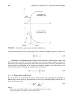
Suppose these modules are separated by a horizontal cut (i.e., heights must be added and widths
must be maxed). The width distribution list of the new rectangle is {(3, .18), (4, .02), (5, .5), (6, .3)}
and its height list is {(9, .2), (10, .5 ), (11, .3)}.
Repeating this process as the area evaluation algorithm traverses the slicing tree in a bottom-up
fashion finally results in distribution lists for chip height and width. The authors use these quantities
to compute a cost function that is the combination of expected area and standard deviation of area.
Including standard deviation in the cost function makes it more likely that the area of the floorplan
obtained by statistical floorplanning is close to the area of the final solution (i.e., after module
dimensions have all been finalized) relative to minimizing expected area alone. The paper also
considers a combined height/width distribution list (e.g., {(4, 5, .3), (6, 3, .7)}means that a module
has height 4 and width 5 with a pr obability of .3 and a height of 6 and a width of 3 with probability
of .7). This is a more realistic formulation, but experimental results have been more promising with
the separate distribution lists.
12.7 FLOORPLANNING FOR MANUFACTURABILITY
Floorplanning, as we have defined it so far, is concerned with the arrangement of components
within a single chip. In this section, we discuss a floorplanning-like problem that arises because of
the economics associated with manufacturing a chip. Recall that several chips can be manufactured
from a single wafer.To do this, a m ask set has to be prepared for the wafer.Thecost of creating a mask
set is substantial. For high-volume manufacturing (i.e., when many chips of the same type are to be
produced), thisone-timecost (X) is amortized overthenumber of chips (c) produced. For low-volume
manufacturing (few chips have to be produced), the cost per chip X/c becomes prohibitive. The
multiple project reticle concept addresses this problem for low-volume manufacturing by departing
from the assumption that all of the chips on a wafer have to be of the same type. Instead, different
chips (p ossibly sent to the fabrication facility b y different companies) are placed in a reticle. Several
copies of the reticle are arranged in rows and columns on a single wafer. The mask cost X can now
be spread out among the different companies. Suppose there are ten different chips from different
companies on a wafer, then the mask cost for each company is X/10. This is amortized over the
number of chips resulting in a cost per chip of X/10c.
However, this approach presents some new challenges. These differentchips have to be extracted
from the wafer by cutting (dicing) the wafer. Existing wafer dicing technologies are somewhat
restrictive, making chip location s o n the reticle vital to optimizing the chip yield. For example, the
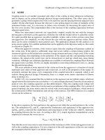
side-to-sidewafer dicing technology cuts the wafer using horizontaland vertical cutlines that traverse
the entire length of the wafer (Figure 12.8). Within a given reticle, these lines may either cut through
dies rendering them useless or might leave large margins making the dies unacceptably large.
There are several associated algorithmic problems. The reticle floorplanning formulation pro-
poses that we comp ute a floorplan and positions of the cutlines assuming a side-to-side wafer dicing
technology. In Ref. [47], both reticle area and wafer yield were optimized using SA. In Ref. [48],
the yield was treated as a constraint and the reticle area was optimized. This strategy, coupled with
a branch-and-bound algorithm, resulted in better solutions than those in Ref. [47]. To further reduce
fabrication cost, projects requiring different num bers of metal layers can be put on the same shuttle.
In Ref. [49], Chen et al. proposed an integer linear programming (ILP)-based floorplanner shuttle
runs consisting of projects of different desired processes.
Another problem associated with reticle floorplanning was considered by Xu et al. [50]. In this
variation, the objective is to c ompute a floorplan that optimizes area and a quantity called postCMP
oxide topography variation. Minimizing this quantity provides the process with a larger margin.
PostCMP oxide topography variation is closely related to the feature density. One technique for
reducing the variation in feature density is to insert dummy features into the design. The floorplanning
algorithm uses SA on slicing floorplans with a cost function that approximates the topography
variation. (Topography variation minimization can be formulated as a linear programming problem,
Alpert/Handbook of Algorithms for Physical Design Automation AU7242_C012 Finals Page 253 24-9-2008 #16
Recent Advances in Floorplanning 253
Reticle
Wafer
Cutting line
Die
FIGURE 12.8 Illustration of reticle floorplanning. A wafer contains many reticles, each of which contains
several dies in an identical configuration. The reticle floorplanning problem asks how these dies should be
configured in the reticle, given that the wafer will be diced using horizontal and vertical lines that cut through
the entire wafer.
but this is too time consuming to include in the SA loop.) SA is followed by a step that slides or
rotates the chip and by a third step that inserts a dummy feature.
12.8 CONCLUDING REMARKS
This chapter has been an effort to try and capture as much floorplanning research as possible with a
bias toward newer and inter esting problem formulations that are likely to be significant in practice.
We apologize in advance for any omissions.
ACKNOWLEDGMENTS
The authors thank Yao-Wen Chang, Tung-Chi Chen, Igor Markov, and Sachin Sapatnekar for
carefully reviewing the manuscript and suggesting improvements.
REFERENCES
1. A.B. Kahng, Classical floorplanning harmful? Proceedings of the 2000 International Symposium on
Physical Design, April 9–12, San Diego, CA, pp. 207–213, 2000.
2. J.L. Hennessy and D. Patterson, Computer Architecture: A Quantitative Approach, Fourth edn. Morgan
Kaufman, 2007.
3. S.N. Adya and I.L. Markov, Fixed-outline floorplanning: Enabling hierarchical design, IEEE T ransactions
on Very Large Scale Integration Systems, Vol. 11, No. 6, pp. 1120–1135, 2003. (ICCD 2001).
4. C T. Lin, D S. Chen, and Y W. Wang, Modern floorplanning with boundary and fixed-outline constraints
via genetic clustering algorithm, Journal of Circuits, Systems, and Computers, Vol. 15, pp. 107–128, Feb.
2006. (ASPDAC 2004).
5. T C. Chen and Y W. Chang, Modern floorplanning based on B
∗
-tree and fast simulated annealing, IEEE
Transactions on Computer-Aided Design of ICs and Systems, Vol. 25, pp. 637–650, Apr . 2006. (ISPD 2005).
6. D. Mehta and N. Sherwani, On the use of flexible, rectilinear blocks to obtain minimum-area floorplans
in mixed block and cell designs, ACM Transactions on Design Automation of Electronic Systems,Vol.5,
pp. 82–97, Jan. 2000.
Alpert/Handbook of Algorithms for Physical Design Automation AU7242_C012 Finals Page 254 24-9-2008 #17
254 Handbook of Algorithms for Physical Design Automation
7. Y. Feng, D. Mehta, and H. Yang, Constrained floorplanning using network flows, IEEE Transactions on
Computer-Aided Design of ICs and Systems, Vol. 23, No. 4, pp. 572–580, 2004. (ISPD 2003).
8. Y. Feng and D. Mehta, Constrained floorplanning with whitespace, in VLSI India, 17th International
Conference on VLSI Design, Mumbai, India, 2004.
9. Y. Feng and D. Mehta, Module relocation to obtain feasible constrained floorplans, IEEE Transactions on
Computer-Aided Design of ICs and Systems, Vol. 25, pp. 856–866, 2006.
10. S. Liao, M. Lopez, and D. Mehta, Constrained polygon transformations for incremental floorplanning,
ACM T ransactions on Design Automation of E lectronic Systems, Vol. 6, Jul. 2001.
11. H M. Chen, H. Zhou, D.F. Wong, H.H. Yang, and N. Sherwani, Integrated floorplanning and interconnect
planning, in International Conference on Computer-Aided Design, San Jose, CA, pp. 54–57, 1999.
12. S.T.W. Lai, E.F.Y. Young, and C.C.N. Chu, A ne w and efficient congestion ev aluation model in floorplan-
ning: Wire density control with twin binary trees, in Design Automation and Test in Europe, in Europe
Conference and Exposition, 3–7 March, Munich, Germany, pp. 856–861, 2003.
13. C. Shen and C. Chu, Accurate and efficient flow based congestion estimation in floorplanning, in Asian
and South Pacific Design Aut o mation Conference , pp. 671–676, 2004.
14. F. Shahrokhi and D.W. Matula, The maximum concurrent flow problem, Journal of the ACM, 37(2),
318–334, 1990.
15. C.W. Sham and F.Y. Young, Routability-driven floorplanner with buffer block planning, IEEE Tr ansactions
on Computer-Aided Design of ICs and Systems, Vol. 22, pp. 470–480, Apr. 2003. (ISPD 2002).
16. Y. Ma, X. Hong, S. Dong, S. Chen, C K. Cheng, and J. Gu, Buffer planning as an integral part of floor-
planning with consideration of routing congestion, IEEE Transactions on Computer-Aided Design of ICs
and Systems, Vol. 24, pp. 609–621, Apr . 2005. (ISPD 2003).
17. J. Cong, T. Kong, and Z. Pan, Buffer block planning for interconnect planning and prediction, IEEE
Transactions on Very Lar ge Scale Integration Systems, Vol. 9, pp. 929–937, Dec. 2001. (ICCAD 1999).
18. X. Tang and D.F. Wong, Network flow based buf fer planning, Integration, Vol. 30, No. 2, pp. 143–155,
2002. (ISPD 2000).
19. P. Sarkar, V. Sundararaman, and C K. Koh, Routability-driven repeater block planning for interconnect-
centric floorplanning, IEEE Transactions on Computer-Aided Design of ICs and Systems, Vol. 20,
pp. 660–671, May 2001. (ISPD 2000).
20. H. Xiang, X. Tang, and M.D.F. Wong, Bus-driven floorplanning, IEEE Transactions on Computer-Aided
Design of ICs and Systems, Vol. 23, No. 11, pp. 1522–1530, 2004. (ICCAD 2003) .
21. J.H.Y. Law and E.F.Y. Young, Multi-bend bus driven floorplanning, in International Symposium on Physical
Design, San Francisco, CA, pp. 113–120, 2005.
22. J. Cong,A. Jagannathan, G. Reinman,and M. Romesis,Microarchitecture evaluation with physi calplanning,
in Proceedings of the 40th Design Automation Conference, Anaheim, CA, June 2–6, 2003.
23. C. Long, L.J. Simonson, W. Liao, and L. He, Floorplanning optimization with trajectory piecewise-
linear model for pipelined interconnects, in Design Automation Conference, San Diego, CA, June 7–11,
pp. 640–645, 2004.
24. M.R. Casu and L. Macchiarulo, Throughput-driv en floorplanning with wire pipelining, IEEE Transactions
on Computer-Aided Design of ICs and Systems, Vol. 24, pp. 663–675, May 2005. (ISPD 2004).
25. M.R. Casu and L. Macchiarulo, Floorplan assisted data rate enhancement through wire pipelining: A real
assessment, in International Symposium on Physical Design, pp. 121–128, 2005.
26. M. Ekpanyapong, J.R. Minz, T. Watewai, H H. Lee, and S.K. Lim, Profile-guided microarchitectural
floorplanning for deep submicron processor design, IEEE Transactions on Computer-Aided Design of ICs
and Systems, Vol. 25, No. 7, pp. 1289–1300, 2006. (DAC 2004).
27. A. Jagannathan, H. Yang, K. Konigsfeld, D. Milliron, M. Mohan, M. Romesis, G. Reinman, and J. Cong,
Microarchitecture evaluation with floorplanning and interconnect pipelining, in Asian and South Pacif ic
Design Automation Conference, Shanghai, China, January 18–21, 2005.
28. V. Nookala, Y. Chen, D.J. Lilja,
a
nd S.S. Sapatnekar, Microarchitecture-aware floorplanning using a sta-
tistical design of experiments approach, in Design Automation Confer ence, San Diego, CA, June 13–17,
2005.
29. V. Nookala, Y. Chen, D.J. Lilja, and S.S. Sapatnekar, Comparing simulation techniques for
microarchitecture-aware floorplanning, in IEEE International Symposium on Performance Analysis of
Systems and Software, A ustin, TX, March 20–22, 2006.
Alpert/Handbook of Algorithms for Physical Design Automation AU7242_C012 Finals Page 255 24-9-2008 #18
Recent Advances in Floorplanning 255
30. Y W. Wu, C L. Yang, P H. Yuh, and Y W. Chang, Joint exploration of architectural and physical design
spaces with thermal consideration, in International Symposium on Low Power Electronics and Design,San
Diego, CA, A ugust 8–10, pp. 123–126, 2005.
31. J S. Yim, S O. Bae, and C M. Kyung, A floorplan-based planning methodology for power and clock
distribution in ASICs, in Proceedings of Design Automation Conference, New Orleans, LA, June 21–25,
pp. 766–771, 1999.
32. C W. Liu and Y W. Chang, Power/ground network and f loorplan cosynthesis for fast design convergence,
IEEE Transactions on Computer-Aided Design of ICs and Systems, Vol. 26, pp. 693–704, Apr. 2007.
(ISPD 2006).
33. L. Cheng and M.D.F. Wong, Floorplan design for multimillion gate FPGAs, IEEE Transactions on
Computer-Aided Design of ICs and Systems, Vol. 25, pp. 2795–2805, Dec. 2006. (ICCAD 2004).
34. Y. Feng and D. M ehta, Heterogeneous floorplanning for FPGAs, in VLSI India, Hyderabad, India, 3–7
January 2006.
35. K. Bazar gan, R. Kastner, and M. Sarrafzadeh, 3-D floorplanning: Simulated annealing and greedy place-
ment methods for reconfigurable computing systems, in Design Automation for Embedded Systems,
2000. (RSP 99).
36. L. Cheng, L. Deng, and M.D.F. Wong, Floorplanning for 3D VLSI design, in Asian and South Pacific
Design Automation C onference, Shanghai, China, January 18–21, 2005.
37. J. Cong, J. Wei, and Y. Zhang, A thermal-driven floorplanning algorithm for 3D ICs, in International
Conference on Computer-Aided Design, San Jose, CA, November 7–11, 2004.
38. F. Balasa and K. Lampaert, Symmetry within the sequence-pair representation in the context of placement
for analog design, IEEE Transactions on Computer-Aided Design of ICs and Systems, Vol. 19, pp. 721–731,
July. 2000. (DAC 1999).
39. F. Balasa and S.C. Maruvada, Using non-slicing topological representations for analog placement, IEICE
Transactions on Fundamentals of Electronics, Communications and Computer Sciences, Vol. E84-A,
pp. 2785–2792, Nov. 2001. (ASPDAC 2001).
40. S.C. Maruvada, K. Krishnamoorthy, F. Balasa, and L.M. Ionescu, Red-black interval trees in device-level
analog placement, IEICE Tr ansactions on Fundamentals of Electronics, Communications and Computer
Sciences, Vol. E86-A, pp. 3127–3135, Dec. 2003. (ASPDAC 2003).
41. F. Balasa, S.C. Maruvada, and K. Krishnamoorthy, On the exploration of the solution space in analog
placement with symmetry const raints, IEEE Transactions on C omputer-Aided Design of ICs and Systems,
Vol. 23, pp. 177–191, Feb. 2004. (ICCAD 2002).
42. J M. Lin, G M. Wu, Y W.Chang, and J H. Chang, Placement with symmetry constraints for analog layout
design using TCG-S, in Proceedings of ACM/IEEE Asia South Pacific Design A utomation Conference,
Shanghai, China, January 18–21, pp. 1135–1138, 2005.
43. S. Kouda, C. Kodama, and K. Fujiyoshi, I mproved method of cell placement with symmetry constraints for
analog IC layout design, in Proceedings of ACM International Symposium on Physical Design, San Jose,
CA, April 9–12, 2006.
44. Y C. Tam, E.F Y. Young, and C. Chu, Analog placement with symmetry and other placement constraints,
in International Conference On Computer Design, Las Vegas, N V, June 26–29, pp. 349–354, 2006.
45. P H. Lin and S C. Lin, Analog placement based on novel symmetry-island formulation, in Design
Automation Conference, San D ie go, CA, June 4–8, 2007.
46. K. Bazargan, S. Kim, and M. Sarrafzadeh, Nostradamus: A floorplanner of uncertain design, IEEE
Transactions on Computer-Aided Design of ICs and Systems, Vol. 18, pp. 389–397, Apr. 1999. (ISPD 1998).
47. A.B. Kahng, I.I. Mandoiu, Q. Wang, X. Xu, and A. Zelikovsky, Multiproject reticle floorplanning and wafer
dicing, in International Symposium on Physical Design, Phoenix, AZ, pp. 70–77, 2004.
48. A.B. Kahng and S. Reda, Reticle floorplanning with guaranteed yield for multi-project wafers, in
International Conference On Computer D esign, San Jose, CA, October 11–13, pp. 106–110, 2004.
49. C C. Chen and W K. Mak, A multi-technology-process reticle floorplanner and wafer dicing planner for
multi-project wafers, in Asian and South Pacific Design Automation Confer ence, Yokohama, Japan, January
24–27, pp. 777–782, 2006.
50. G. Xu, R. Tian, D.Z. Pan, and M.D.F. Wong, CMP aware shuttle mask floorplanning, in Asian and South
Pacific Design Automation Conference
, Shanghai, China, January 18–21, pp. 1111–1115, 2005.
Alpert/Handbook of Algorithms for Physical Design Automation AU7242_C012 Finals Page 256 24-9-2008 #19
256 Handbook of Algorithms for Physical Design Automation
BIBLIOGRAPHY
1. S.N. Adya and I.L. Markov, Consistent placement of macro-blocks using floorplanning and standard-cell
placement, ACM Transactions on Design Automation of Electronic Systems, Vol. 10, Jan. 2005. (ISPD
2002).
2. J. Cong, M. Romesis, and J. Shinnerl, Fast floorplanning by look-ahead enabled recursive bipartitioning,
IEEE Transactions on Computer-Aided Design of ICs and Systems, Vol. 25, pp. 1719–1732, Sept. 2006.
(ASPDAC 2005).
3. J. Crenshaw, M. Sarrafzadeh, P. Bannerjee, and P. Prabhakaran, An incremental floorplanner, in GLSVLSI,
Ann Arbor, M I, pp. 248–251, 1999.
4. A. Ranjan, K. Bazargan, and M. Sarrafzadeh, Fast hierarchical floorplanning with congestion and timing
control, IEEE Transactions on Very Large Scale Integration Systems, Vol. 9, No. 2, pp. 341–351, 2001.
(ICCD 2000).
5. F. Rafiq, M. Chrzano wska-Jeske, H.H. Yang, and N. Sherwani, Bus-based integrated floorplanning, in
Pr oceedings of the IEEE Symposi u m on Circuits and Systems, Scottsdale, AZ, pp. 875–878, 2002.
6. F. Rafiq, M. Chrzano wska-Jeske, H.H. Yang, M. Jeske, and N. Sherwani, Integrated floorplanning with
buffer/channel insertion for bus-based designs, IEEE Transactions on Computer-Aided Design of ICs and
Systems, Vol. 22, No. 6, pp. 730–741, 2003. (ISPD 2002).
7. Y.M. Fang and D.F. Wong, Simultaneous functional-unit binding and floorplanning, in International
Conference on Computer-Aided Design, San Jose, CA, pp. 317–321, 1994.
8. M. Moe and H. Schmit, Floorplanning of pipelined array modules using sequence pairs, in International
Symposium on Physical Design, Monterey, CA, April 6–9, 2003.
Alpert/Handbook of Algorithms for Physical Design Automation AU7242_C013 Finals Page 257 24-9-2008 #2
13
Industrial Floorplanning
and Prototyping
Louis K. Scheffer
CONTENTS
13.1 Introduction 257
13.1.1 Floorplanning in the Design Flow 258
13.1.2 Evolution of Block-Based Designs [4] 259
13.2 History 259
13.2.1 Historyof Pin Assignment 261
13.2.2 History of Timing Budgets 261
13.2.3 Academic versus Industrial Floorplanning 261
13.3 Use of Hierarchy 261
13.3.1 Is Hierarchical DesignLess Efficient? 262
13.3.2 Logical versus Physical Hierarchy 262
13.4 Pin Assignment and Timing Budgeting 263
13.5 Routability Analysis 264
13.6 Bufferand Flip-Flop Insertion 265
13.7 Estimating Parasitics and Timing 265
13.8 Power Supply Design 266
13.9 ECOs and Accounting for Changes 267
13.10 Working with Incomplete and Inconsistent Designs 268
13.11 Conclusions and Future Work 268
Acknowledgments 270
References 270
13.1 INTRODUCTION
Industrial floorplanning and prototyping consist of the steps needed after the chip logic is defined,
but before the final detailed implementation of a production chip. Several of the steps, such as pure
block placement and mixed b lock and cell placement (also called the boulders and dust problem),
have received considerable academic interest and are covered in other sections. This chapter instead
concentratesonthepracticalproblemsthatmustbesolvedinthefloorplanningoflargeindustrialchips.
In this chapter we assume the chips to be designed consist of predefined blocks and standard cells.
Predefined blocks (commonly called IP blocks, where IP stands for intellectual p roperty) commonly
include memories, processorsand analogfunctions,and are presented to the designer as givens. Their
placement and orientation must be decided, but their contents cannot be changed. IP blocks come in
a wide variety of shapes and sizes, but are typically relatively large, perhaps the equivalent of a few
thousand to a few million gates. Standard cells, by contrast, are very small, usually incorporating just
one to a few logic gates. Usually they are of a uniform height (hence standard) and designed to be
abutted into rows. A crucial distinction in a typical design flow is that the IP blocks are selected by
the designer, and cannot be changed by the automatic tools, whereas the standard cells, are normally
257
Alpert/Handbook of Algorithms for Physical Design Automation AU7242_C013 Finals Page 258 24-9-2008 #3
258 Handbook of Algorithms for Physical Design Automation
generatedb y logic synthesis [1],andcan be freely modifiedbythe tools as long as the logicalfunction
specified by the RTL is preserved.
A floorplanand a prototype are two different approximate versions of a chip, at differentlevels of
abstraction. The floorplan is the more abstract of the two, consisting of just a chip outline, placement
and orientation of the hard blocks, an IO placement, sites where the standard cells can go, and an
approximate power grid design. The blocks may be hard, or fully defined, or may be blocks that
are still under construction. These are commonly called soft if their size or aspect ratio is not fully
decided, or black or gray boxes if their size is fixed but their contents unknown. (In the terminology
of floorplanning, a black box is a cell where only the inputs, outputs, and function are known. By
analogy, white and gray boxes have contents fully and partially defined, respectively. Note that the
color of a box may vary according to purpose—the same block may be a black box for placement, a
gray box for timing, but a white box for logic verification.)
A prototype consists of everything from the floorplan, plus a detailed placement and at least a
rough route (normallyincluding at least layer and track assignment). The goal is to enable reasonably
accurate extraction and timing verification, and hence show a design is feasible and ready for the
more time-consuming steps of final placement and routing. The final detailed implementation may
or may not follow the prototype.
Like placement, a good floorplan or prototype is not unique. Typically, there are many different
possible floorplans for the same design, of comparable quality. One of the major questions, as in
placement, is how do you know you have got a good floorplan, compared with what might be
possible? This situation is even worse than the situation in placement, where there are at least a few
examples where the optimum solution is known [2].
13.1.1 FLOORPLANNING IN THE DESIGN FLOW
Design of a modern chip involves many steps. First, the exact function of the chip must be defined,
and shown to be correct. The formal definition of the function is usually specified in RTL, and
proving it correct is done by simulation, formal verification, and a host of other techniques. These
steps are collectively r eferred to as front-end design.
The RTL from the front-end process then goes to the back end where it is turned into a detailed
implementation. Normally, this involves mapping the function into an interconnected set of logic
gates (by logic synthesis), followed by p lacement, routing, extraction, timing analysis, and design
rule checking, and ultimately the fabrication of the masks, and then ICs.
In cases where engineering margins of performance, power, and cost are large, the front and back
ends can be largely independent. In many cases, however, they interact fairly strongly, particularly
when some feature of th e RTL is difficult or impossible to implement in the back end. This interaction
is made worse by the differing expertises involved. Most front-end designers are not familiar with the
back-end tools, and do not have time to run them in any case. Most back-end designers do not have
the expertise to change the RTL, even if they were allowed to do so. Floorplanners are an attempt to
bridge this gap with a tool accessible to both sides.
Floorplanningdecides the overall layout of the chip, and is used early in the chip design flow [3],
when the design is malleable and all fixes are possible. Normally it is used by a front-end user, or a
back-end expert working in close cooperation with a front-end group. One of the main objectives of
floorplanningis helping both the front- and back-end users understand the design. Which constraints
are easy, and which hard? Does it meet timing? Routability? Has enough routing resource been
allocated to the power supplies? Will the RTL work as is, or are changes needed to make it feasible to
meet the design constraints using the specified process and library? Because one of the main tasks of
a floorplanner is diagnostics (where is the routing hard, and why? Why is the timing hard to meet?),
easy-to-use graphical user interfaces (GUIs) and easy-to-understand feedback are critical.
Because one of the main points of floorplanning is to understand the d esign as early as possible,
a crucial featu re of a floorplanner is the ability to work with incomplete designs. Missing blocks,
Alpert/Handbook of Algorithms for Physical Design Automation AU7242_C013 Finals Page 259 24-9-2008 #4
Industrial Floorplanning and Prototyping 259
incompleteconstraints, and even missing technologyinformationmust be h andled, often by allowing
designers to enter estimates for the missing data.
OncetheRTLisdeemed complete,or nearlyso,thenextstepisprototyping.Thisisafast(andoften
rough) pass through the entire physical design process of synthesis, placement, routing, extraction,
and timing analysis. This quick pass is meant to verify feasibility and completeness before starting on
the lengthy production-quality physical design steps. The prototype design produced may or may not
form theb asis ofthe finalimplementation. Normallyprototypingis donebya back-enduser,o r atleast
someone with experience in placement and routing. Because one of the main reasons for prototyping
is to ensure that everything is ready, it is much less tolerant of missing data than a floorplanner. The
prototyper will perform at least a rough version of the final implementation steps, including place
and route, extraction and timing analysis, so all required inputs must be present and consistent. This
includes libraries, the input hardware description language (or HDL), constraints, IP blocks, and so
on. Completion of a successful prototype shows the RTL should no longer need major changes.
Prototyping is also part of a business model for ASIC handoff. In this business model, respon-
sibility for a chip is split among the end customer, who wishes to logically design and sell a chip,
and the ASIC house, who does the detailed implementation and manufacturing. Several costs and
responsibilities are contractually obligated in such a relationship:
• The designer, usually working at the end customer, must supply an RTL that can be practi-
cally implemented in the specified process (even though they do not do this implementation
themselves).
• The ASIC house must quote a price for the detailed implementation. There are normally
additional charges if the RTL changes after implementation starts.
• The ASIC house must quote a price for each chip produced.
Prototyping (and to a lesser extent, floorplanning) helps a great deal with this interface between
companies. The designer uses prototyping to make sure their RTL can be implemented in the specified
process with the needed performance, and to ensure that all is ready for implementation, to avoid
additional charges for later changes. Also, a prototype serves as a concrete example of at least one
way to meet the design goals, though the ASIC house is not normally constrained to follow it. On the
other side, the ASIC house uses prototyping for QA on incoming designs, to make sure all required
information is ther e, and for cost estimates for both the detailed implementation process and the final
chip cost. A prototype, as a physically accurate model, also helps ensure that the chip will fit in the
specified package and can be bonded successfully.
Finally, a floorplanner or prototyper also serves as a central repositor y for data, especially in the
hierarchical design style. The input is the RTL for all groups, libraries, IO files, SDC constraints, and
so on. The output is a similar set of files for each physical block. This implies the use and reading o f
many languages: LEF/DEF, IO specifications, Verilog or VHDL, delay constraints, and so on.
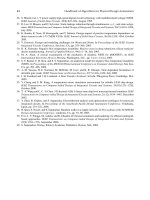
13.1.2 EVOLUTION OF BLOCK-B ASED DESIGNS [4]
Floorplanners were originally built for designs with relatively few blocks, with the chip area dom-
inated by standard cells, as shown in Figure 13.1a. However, as chips have gotten larger, designers
have incorporated larger and larger fractions of blocks. The remaining standard cells, increasing in
number but decreasing in terms of percentage, must be placed into the spaces between the blocks.
An example of such a floorplan is shown in Figure 13.1b. This change in design style has several
implications for the algorithms and methods used in today’s floorplanners.
13.2 HISTORY
When chips were small, and tools primitive, what we currently call a floorplan could be drawn by
hand on a piece of paper. Place and route tools, when used, were only run after the netlist was
Alpert/Handbook of Algorithms for Physical Design Automation AU7242_C013 Finals Page 260 24-9-2008 #5
260 Handbook of Algorithms for Physical Design Automation
(a) (b)
FIGURE 13.1 (a) Standard cell-dominated design on the left and (b) block-dominated design on the right.
(From Wein, E. and Benkoski, J., Electronics Engineering Times, August 20, 2004. With permission.)
finalized. Performance was verified by taking the final placed and routed results, running extraction,
then delay calculation, then timing analysis. Any performance optimizations, or corrections of errors
and omissions, were done using the place or route tool directly.
As chips grew past a few thousand gates, an additional tool began to make sense. Some of tasks
that were not well addressed by the old flow include:
• Designers wished to know if a design was feasible before (or without) doing the final layout
tasks such as a fully detailed power grid.
• Designers wanted to examine the feasibility of a design before all parts were complete.
• Designers wanted to divide a design up into two or more sections, each of which could be
treated separately.
• Designers wanted to understand where there design was easily implemented, and where
there were problems, early in the design cycle when RTL changes are still relatively
easy.
Floorplanners were invented to address these needs. Many of the initial uses of floorplanning envi-
sioned it as part o f a suite of integrated tools, such as VIVID [5,6], or the internal tools of DEC [7],
or CHEOPS [8]. By 1986, standalone floorplanners such as Mason were available [9].
In the late 1990s, as designs became bigger yet, they often ran into problems in detailed imple-
mentation even though they had what appeared to be a good floorplan. In particular, problems often
only showed up after detailed routing, extraction, and timing were complete, because many charac-
teristics of the final design are heavily influenced by the details of the routing. However, detailed
placement, routing, extraction, and verification often took a week or more—not unreasonable for the
final implementation, but too long for effective feedback to the earlier stages of the design process.
The technical solution was to do a very fast but fully detailed placement, followed by a very fast
(but rough) detailed route, and a fast approximate RC extract. If timing analysis on this indicated
all was well, then the relatively lengthy detailed implementation process could begin. A floorplan
that was verified through these additional steps was sometimes called a virtual silicon prototype,
and the process called prototyping. See Goering for an early reference [10], Chao and Lev [11] for
an informal explanation of the importance of detailed wiring, and Dai et al. [12] for a more formal
description of the process.
Alpert/Handbook of Algorithms for Physical Design Automation AU7242_C013 Finals Page 261 24-9-2008 #6
Industrial Floorplanning and Prototyping 261
13.2.1 HISTORY OF PIN ASSIGNMENT
Early on, printed wiring boards (PWBs) served as modules. Assigning pins on these modules was
the equivalent of pin assignment in IC floorplanners. This was does as early as 1972 [13]. For ICs,
this problem was only seriously addressed in the 1980s.
By 1984,thepinassignment problemwas explicitlyaddressed [14]. By 1989,pinassignmentwas
being combined with global routing [15,16]. By 1990, it was combined with floorplanning [17,18],
and by 2002 with buffer planning [19]. See Section 13.4 for more details.
13.2.2 HISTORY OF TIMING BUDGETS
Time budgeting was first addressed in the context of breaking a path delay into individual net
delays, as in Ref. [20]. Many other approaches to this have been developed [21]. Then budgeting
was extended to hierarchical design, for example, by Venkatesh [22] or Kuo and Wu [23]. In a
floorplanner, it makes sense to use the hierarchy information as well [24].
13.2.3 ACADEMIC VERSUS INDUSTRIAL FLOORPLANNING
Although they both have activities called floorplanning, industry and academia mean very different
things by this term. In academia, floorplanning refers primarily to automatic placement of pure block
designs,or designs includinglarge fractionsof blocks, with objectives of good packingand minimum
wirelength. A related term, floorplacement, refers to the automatic simultaneous placement of blocks
and standard cells [25,26].
In contrast, in industrial floorplanning, manual input is allowed if not encouraged, and the main
goals are timing and routability, with area an d wirelength tr eated as means to an end , and n ot an
objective by themselves. Industrial floorplanning includes, and is often dominated by, practical con-
cerns such as power grid design, dealing with partially specified or contradictory data, multivoltage
support for power reduction, buffer insertion, ease of clock tree design, and so on.
13.3 USE OF HIERARCHY
Floorplanning and prototyping may be flat or hierarchical. In a flat floorplan, the entire design is
treated as a single problem, and any cell or block can be placed at any location in the design. There
is no need to assign cells and pins to the blocks, or create block budgets for timing or power. This
flat design style is conceptu ally straightforward and provides maximum implementation flexibility.
However, it has several disadvantages, especially for large designs. It may stress the limits of tools
(which often cannot handle a large design flat) as well as humans, who may not be able to easily
understand such a design. Because every detail of the design interacts, there may be no easy way to
divide the work among teams. Flat design may well make changes more difficult, because they are
less localized, which can also impact design closure [27]. For these and other reasons, many chips
are designed hierarchically. In this case, the chip surface is divided into areas, commonly called
blocks. Each block represents an independent design problem—all cells assigned to the block must
be placed inside it, and all wires purely internal to the block must be routed within its boundary.
Signals that connect to the rest of the design are brought to pins, where the routing from the rest of
the design will connect. These pins must be assigned locations and layers for each block, and each
block must be assigned a definite size and location within the chip. All design constraints must be
budgeted among the blocks. Foremost among these constraints are timing and power. The budgeting
process is crucial, in particular, one infeasible budget (among tens of thousands of pins) can make
the whole design infeasible, where it might be easily completed using a flat flow.
There are also intermediate design styles, intended to combine the advantages of flat and hier-
archical design. For example, placement might be hierarchical, to limit the scope of changes, but
routing done flat, to avoid the need for pin assignment. A similar approach is a flat floorplan with
regions. In this particular case, the cells are confined to specific regions as in a hierarchical design,