- Trang chủ >>
- Khoa Học Tự Nhiên >>
- Vật lý
Handbook of algorithms for physical design automation part 61 pdf
Bạn đang xem bản rút gọn của tài liệu. Xem và tải ngay bản đầy đủ của tài liệu tại đây (176.14 KB, 10 trang )
Alpert/Handbook of Algorithms for Physical Design Automation AU7242_C028 Finals Page 582 30-9-2008 #15
582 Handbook of Algorithms for Physical Design Automation
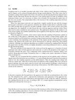
It has been demonstrated that K can be used to trade off the cost function, the merging operation,
and even sink initialization. In practice, we can first optimize all nets that need buffering with K = 1,
which limits the use of scarce resources. After perfor ming a timing analysis, those nets that still have
negative slack can be reoptimized with a smaller value of K, e.g., 0.7. This process of reoptimizing
and gradually reducing can continue until, say, K = 0.1.
28.5.4 RELATING BUFFERING CANDIDATE LOCATIONS TO LAYOUT ENVIRONMENT
While the previous algorithms are considering the routing tree adjustment, the following algorithm
focuses on buffer insertion candidate selection for congestion reduction.
Van Ginneken style algorithm assumes that a set of buffer insertion candidate locations are
predetermined for the given topology. The most common method for selecting insertion points is to
choose them at regular intervals. Alpert and Devgan [15] show how the quality of results is affected
by the degree of wire segmenting that is performed on the topology. For example, Figure 28.15a
shows uniform segmenting for a Steiner tree with three sinks and a single blockage. For these regions
for which buffer insertion is forbidden, one simply avoids inserting buffer candidate locations on
top of the blockage. In Figure 28.15b, one can find the same uniform segmenting scheme, but with
finer spacing. The additional buffer insertion locations could potentially improve the timing for the
buffered net, for additional runtime cost. In Figure 28.15c, one can use roughly the same number of
buffer insertion candidates as in uniform segmenting, but spacing them asymmetrically.The purpose
is not to improve timing perfor mance but rather to bias van Ginneken style algorithm to insert buffers
in regions of the design that are more favorable, such as areas with lower congestion cost.
To accomplish this buffer candidate selection, Ref. [18] applies a linear time and linear mem-
ory shortest path algorithm. The algorithm constructs a directed acyclic graph (DAG) over the
set of potential candidate locations and chooses a subset by constructing a shortest path via a
topological sort.
Let L be the maximum allowable tiles in the tile gr aph (described in Section 28.4.1) between
consecutive buffers, which could be determined by a maximum allowable slew constraint. If buffers
are placed at a distance greater than L tiles away, then an electrical violation results or performance
is significantly sacrificed. On the basis of L, edges are created by connecting the tiles which are no
greater than L tiles away fro m each other. The edge represents a pair of consecutive buffer candidates
on the fixed routing tree.
Moreover, we define S to be the desired number of tiles between consecutive buffer insertion
candidates, which is chosen by the user to obtain the desired timing performance/CPU trade-off.
For example, Figure 28.15a has a value that is twice that of Figure 28.15b. For asymmetric spacing,
a penalty is associated for spacin g tiles either closer to or further from the desired spacin g S.We
define a function pen(x, S, L) =
(x−S)
2
(L−S)
2
that assigns a penalty cost on an edge when the distance x
(a) (c)(b)
FIGURE 28.15 Giv en a fixed topology, one can se gment wires uniformly via either (a) coarse or (b) finer
spacing. Reference [18] uses asymmetric segmenting (c) based on the design characteristics.
Alpert/Handbook of Algorithms for Physical Design Automation AU7242_C028 Finals Page 583 30-9-2008 #16
Buffering in the Layout Environment 583
between tiles is not equal to S. Together with the congestion consideration, the total cost of a path
is the summation over the penalty cost of all edges and the congestion cost of all tiles on the path.
Hence, the problem can be solved by a topological sort, which finds the minimum cost path from
the source to all sinks. By the application of this preprocessing technique, buffers finally inserted
significantly improve the overall design congestion with virtually no impact on either computation
time or buffered net delays. In fact, because the preprocessingis more selective of the potential buffer
insertion candidates, the final buffer insertion process can be speed up dramatically.
REFERENCES
1. H. Zhou, D. F. Wong, I. -M. Liu, and A. Aziz. Simultaneous routing and buffer insertion with restrictions on
buffer locations. IEEE Tr ansactions on Computer-Aided Design, 19(7):819–824, July 2000 (ICCD 2001).
2. S. -W. Hur, A. Jagannathan, and J. Lillis. Timing driven maze routing. In Proceedings of the ACM
International Symposium on Physical Design, Monterey, CA, pp. 208–213, 1999.
3. A. Jagannathan, S. -W. Hur, and J. Lillis. A fast algorithm for context-aware buffer insertion. In Proceedings
of the ACM/IEEE Design Automation Conference, Los A ngeles, C A, pp. 368–373, 2000.
4. M. Lai and D. F. Wong. Maze routing with buffer insertion and wiresizing. In Proceedings of the ACM/IEEE
Design Automation C onference, Los Angeles, CA, pp. 374–378, 2000.
5. C. J. Alpert, G. Gandham, J. Hu, J. L. Ne ves, S. T. Quay, and S. S. Sapatnekar. A Steiner tree construction for
buffers, blockages, and bays. IEEE Transactions on Computer-Aided D esign, 20( 4):556–562, April 2001.
6. J. Hu, C. J. Alpert, S . T. Quay, and G. Gandham. Buffer insertion with adaptive blockage avoidance. IEEE
Transactions on Computer-Aided Design, 22(4):492–498, April 2003.
7. L. P. P. P. van Ginneken. Buffer placement in distributed RC-tree networks for minimal Elmore delay.
In Pr oceedings of the IEEE International Symposium on Circuits and Systems, New Orleans, LA,
pp. 865–868, 1990.
8. J.Cong andX. Yuan. Routing tree construction underfix edbuffer locations. InProceedings of the ACM/IEEE
Design Automation C onference, Los Angeles, CA, pp. 379–384, 2000.
9. X. Tang, R. Tian, H. Xiang, and D. F. Wong. A new algorithm for routing tree construction with buffer inser-
tion and w ire sizing under obstacle constraints. In Proceedings of the IEEE/ACM International Conference
on Computer-Aided Design, San Jose, CA, pp. 49–56, 2001.
10. S. Dechu, Z. C. Shen, andC. C. N. Chu. An efficient routing tree construction algorithm with buffer insertion,
wire sizing and obstacle considerations. IEEE Transactions on Computer-Aided Design, 24(4):600–608,
April 2005.
11. C. J. Alpert, G. Gandham, M. Hrkic, J. Hu, S. T. Quay, and C. N. Sze. Porosity-aware buffered Steiner
tree construction. IEEE Transactions on CAD of Integrated Circuits and Syst ems, 23(4):517–526, 2004
(ISPD 2003).
12. C. N. Sze, J. Hu, and C. J. Alpert. A place and route aware buffered Steiner tree construction. In Proceedings
of Asia and South Pacific Design Automation Conference, Yokohama, Japan, pp. 355–360, 2004.
13. C. J. Alpert, C. Chu, G. Gandham, M. Hrkic, J. Hu, C. Kashyap, and S. T. Quay. Simultaneous driver sizing
and buffer insertion using delay penalty estimation technique. IEEE Transactions on Computer-Aided
Design, 23(1):136–141, January 2004.
14. C. J. Alpert, J. Hu, S. S. Sapatnekar, and P. G. Villarrubia. A practical methodology for early buffer and
wire resource allocation. In Proceedings of t h e ACM/IEEE Design Automation Conference,LasVegas,NV,
pp. 189–194, 2001.
15. C. J. Alpert and A. Devgan. Wire segmenting for impro ved buffer insertion. In Proceedings of the ACM/IEEE
Design Automation C onference, Anaheim, CA, pp. 588–593, 1997.
16. C. C. N. Chu and D. F. Wong. Closed form sol ution to simultaneous buffer insertion/sizing and wire
sizing. In Proceedings of the ACM International Symposium on Physical Design, Napa Valley, CA,
pp. 192–197, 1997.
17. C. J. Alpert, M. Hrkic, J. Hu, and S. T. Quay. Fast and flexible buffer t rees that navigate the physical
layout environment. In Proceedings of the ACM/IEEE Design Automation Conference, San Diego, CA,
pp. 24–29, 2004.
Alpert/Handbook of Algorithms for Physical Design Automation AU7242_C028 Finals Page 584 30-9-2008 #17
584 Handbook of Algorithms for Physical Design Automation
18. C. J. Alpert, M. Hrkic, and S. T. Quay. A fast algorithm for identifying good buffer insertion candi-
date locations. In Pr oceedings of the ACM International Symposium on Physical Design, Phoenix, AZ,
pp. 47–51, 2004.
19. C. J. Alpert, J. Hu, S. S. Sapatnekar, and C. -N. Sze. Accurate estimation of global buffer delay within
a floorplan. In Proceedings of the IEEE/ACM International Conference on Computer-Aided Design,San
Jose, CA, pp. 706–711, 2004.
Alpert/Handbook of Algorithms for Physical Design Automation AU7242_C029 Finals Page 585 29-9-2008 #2
29
Wire Sizing
Sanghamitra Roy and Charlie Chung-Ping Chen
CONTENTS
29.1 Wire-Sizing Basics 585
29.1.1 Delay and Cross-TalkModeling 586
29.1.2 Parasitics Modeling: Resistance, Capacitance, and Inductance 587
29.2 Wire-Sizing Optimization: Problem Formulation 588
29.2.1 Weighted Delay, Timing Constraints, and Power Consideration 588
29.2.2 Discrete versus Continuous, Uniform versus Nonuniform 588
29.3 Optimization Algorithms 588
29.3.1 Discrete Optimization Algorithm 588
29.3.2 Convex Programming Algorithm 590
29.3.3 Lagrangian Relaxation-Based Algorithm 590
29.3.4 Ensuring the Convexity of Gate Delay Models by Semidefinite Programming 591
29.3.5 Sequential Quadratic Programming Algorithm 592
29.3.6 Variational Calculus-Based Nonuniform Sizing Algorithm 592
29.3.7 Optimal Propagation Speed with Wires 593
29.3.8 High-Order Moment-Based Algorithm 593
29.4 Signal Integrity Optimization Algorithm 594
29.4.1 Noise Aware Optimization 594
References 595
With the rapid shrinking of technology feature size, the interconnect delay occupies a significant
portion of the circuit delay. The improvement of interconnect delay has become an important task.
Without increasing chip transistors, wire sizing has been shown as an effective way to reduce
interconnect delay. In this chapter, we introduce several effective techniques of wire sizing.
29.1 WIRE-SIZING BASICS
With technology scaling and decrease in feature size, interconnect delay has become a dominant
factor in determining system performance. With higher level of integration, the interconnect mod-
eling becomes more complicated as the total on-chip interconnect length increases and there are
multilayered interconnect structures embedded in multiple dielectrics. The resistance per unit length
of the interconnect increases with scaling; supply voltages are also scaled down resulting in slower
global interconnects. Gate delay decreases with the shrink in feature size, whereas interconnect delay
increases. It has been predicted that the interconnect delay can account for over 50 percent of the total
path delay in a circuit. For large high-performance designs, numerous buffers are inserted resulting
in smaller distance between buffers. Buffer insertion in large numbers increases power consumption
dramatically. Because the interconnect delay depends on the wire width, length, and the buffer sizes
and placement, optimally sizing the wires and buffers can help in minimizing the interconnect delay
as well as power consumption.
585
Alpert/Handbook of Algorithms for Physical Design Automation AU7242_C029 Finals Page 586 29-9-2008 #3
586 Handbook of Algorithms for Physical Design Automation
1000 µm
500 µm
500 µm
0.5 µm2 µm
1 µm
10 fF
10 fF
(b)
(a)
Wire assignment 2
Wire assignment 1
FIGURE 29.1 Wire-sizing result comparison.
Now we use an example to explain the effectiveness of wire sizing. As shown in Figure 29.1,
the first wire with length 1000 µm, and width 1 µm with 10 fF load while the second wire with
same wirelength and width 2 µm in the first 500µm and 0.5 µm in the second half. We assume
the unit resistance, unit capacitance, and thickness of the wires are 0.008 ,0.06fF/µ
2
,and1µm,
respectively. The Elmore delay of the two wires are 0.56ps and 0.42 ps, respectively. A 25 percent
delay reduction can be immediately obtained.
Hence modeling and optimization of interconnects is a critical component of the design of d eep
submicron very-large-scaleintegration (VLSI) circuits. Now we present an overview of interconnect
and parasitics modeling.
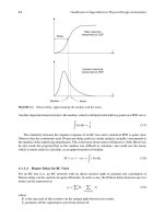
29.1.1 DELAY AND CROSS-TALK MODELING
The Elmore delay model is easy to use and captures the distributed nature of the circuit. However, as
technology scales down to deep submicron levels, the Elmore model becomes inaccurate in signal
modeling, as it cannot incorporate the effects of cross talk and inductance in the circuit. The Elmore
delay only uses the first moment of h(t) to approximatethe circuit response to a step input.For further
accuracy, higher moments of h(t) are used, and these are called moment matching techniques.
The asymptotic waveform evaluation [Pillage 1990] technique uses explicit moment matching
for approximation of the transient response waveform of RLC (consisting o f resistor R, an inductor
L, and a capacitor C) circuits with nonequilibrium initial conditions. It approximates the transfer
function H(s) by a transfer function with q poles of the form
ˆ
H(s) =
q
i=1
k
i
s −p
i
where p
i
are poles and k
i
are residues to be determined. The time domain impulse response is
ˆ
h(t) =
q
i=1
k
i
e
p
i
t
The 2q −1 moments of H(s) can be matched with those of
ˆ
H(s) to determine the poles and residues
in
ˆ
H(s).
Alpert/Handbook of Algorithms for Physical Design Automation AU7242_C029 Finals Page 587 29-9-2008 #4
Wire Sizing 587
L
H
W
Dielectric
Substrate
t
di
FIGURE 29.2 Interconnects.
Passive reduced–order interconnect macromodeling algorithm (PRIMA) [Odabasioglu 1998] is
a moment matching technique for RLC circuits that also preserves the passivity of the system to
maintain stability. The moment-based models have a higher degree of accuracy than the Elmore
delay model, but their computation is more difficult and expensive.
29.1.2 PARASITICS MODELING: RESISTANCE, CAPACITANCE, AND INDUCTANCE
The resistance o f a wire can be estimated using the formula
R =
ρL
A
=
ρL
HW
where as shown in Figure 29.2
ρ is the resistivity
L is the length
W is the width
H is the thickness of the wire
The wire over the substrate can be modeled as a conductor over the ground plane. The parallel plate
capacitance can hence be calculated as
C
pp
=
ε
di
t
di
WL
where
t
di
is the distance to the substrate
ε
di
is the dielectric constant
The othercomponent of thecapacitanceisthefringingcapacitance whichis moredifficultto compute.
The total capacitance is the sum of a parallel plate capacitor of width W −
H
2
and a cylindrical
capacitor of radius H/2. The interconnect inductance can be estimated using the definition v = L
di
dt
.
The inductance L
in
of a conductor can be approximately given by
L
in
= L
µ
0
2π
ln
8t
di
W
+
W
4t
di
where µ
0
is the permeability of free space. Inductive effects in interconnects can be ignored if the
resistance is substantial or if the rise and fall times of the applied signals are slow.
Alpert/Handbook of Algorithms for Physical Design Automation AU7242_C029 Finals Page 588 29-9-2008 #5
588 Handbook of Algorithms for Physical Design Automation
29.2 WIRE-SIZING OPTIMIZATION: PROBLEM FORMULATION
Wire-sizing optimization tries to determine the optimal wire widths for each wire segment in an
interconnect tree to minimize an objective function, which may be the interconnect delay, power, or
a combination of both [Lillis 1995, Chu 1999a, Gao 1999, Tsai 2004, Zhang 2004]. We now discuss
various different types o f objectives in the wire-sizing problem and the different kinds of wire-sizing
problems.
29.2.1 WEIGHTED DELAY, TIMING CONSTRAINTS, AND POWER CONSIDERATION
The delay in an interconnect tree consisting of multiple sinks and a single source can be minimized
by using a weighted sum of delays from the source to each sink, as an objective function. In case
of multiple source nets, we can minimize the weighted sum of delays between multiple source–sink
pairs. Another option is to minimize the maximum delay of the tree. Also with technology scaling,
power consumption has become a major design constraint in current designs. Thus an objective
function consisting of the weighted sum of power and delay can also be minimized in the wire-sizing
problem [Cong 1994, Cong 1996b]. Alternately, instead of minimizing the delay, the wire sizes can
be minimized under maximum delay constraints. Later in the chapter, several approaches illustrate
these different objectives in wire sizing.
29.2.2 DISCRETE VERSUS CONTINUOUS, UNIFORM VERSUS NONUNIFORM
Wire-sizing optimization may be continuous or discrete. In continuous wire sizing, the wire width
h can take any values between the upper and lower bounds as shown in Figure 29.3a. In discrete
wire sizing on the other hand, the wire width must be taken from a discrete set of values as shown
in Figure 29.3b.
In uniform wire sizing, the wire segment is supposed to have a constant width throughout its
length as in Figure 29.3, while in nonuniformwire sizing [Chen 1996], the width of the wire segment
varies along its length as shown in Figure 29.4. Nonuniform wire sizing is discussed later in this
chapter.
29.3 OPTIMIZATION ALGORITHMS
We now describe the different optimization algorithms used in solving the wire-sizing problem.
29.3.1 DISCRETE OPTIMIZATION ALGORITHM
Figure 29.5 shows a routing tree T for a signal net with source N+ and sinks {N
1
, N
2
, N
3
}.Thetree
consists of segments {E1, E2, E3, E4, E5}. sink(T) denotes the set of sinks in T, W is a wire sizing
solution (consisting of wire widths for every segment of T), and t
i
(W) is the delay from source to sink
s
i
under width assignment W. T
v
denotes a subtree rooted at v. For a given edge E,Des(E) denotes
the set of edges in the subtree rooted at E and Ans(E) denotes the set of edges {E
|E ∈ Des(E
)},
(a) Continuous wire sizing (b) Discrete wire sizing
h
h
1
h
4
Upper bound
Lower bound
h
FIGURE 29.3 Continuous versus discrete sizing.
Alpert/Handbook of Algorithms for Physical Design Automation AU7242_C029 Finals Page 589 29-9-2008 #6
Wire Sizing 589
Wire
f(x)
x0
L
FIGURE 29.4 Nonuniform wire.
both excluding E. We n ow describe three important properties [Cong 1993] of optimal wire-sizing
solutions that are used in designing wire-sizing algorithms.
• Monotone property: Given a routing tree T, a wire sizing solution W on T is a monotone
assignment if W
E
≥ W
E
for any pair of segments E, E
such that E ∈ Ans(E
).
• Separability: If the width assignment of the path from the source to a segment E is
given, the optimal width assignment of each subtree branching from E can be carried
out independently.
• Dominance property: A wire size assignment W dominates a wire-size assignment W
if
every segment width in W is greater than or equal to the corresponding segment width in
W
. For a given wire-sizing solution W for the routing tree, and one particular segment
E ∈ T, the local refinement on E is the operation to optimize the width of E wh ile keeping
the widths of the other segments constant. If W
∗
is an optimal wire-sizing solu tion, and if
W dominates W
∗
, then any local refinement of W will also dominate W
∗
.
The discrete wire-sizing problem [Cong 1993] can be formulated as follows:
Given A set of discrete wire widths
{
W
1
, W
2
, , W
r
}
Find An optimal wire width assignment W
To minimize t
(
W
)
=
N
i
∈sink(T)
λ
i
· t
i
(W)
where λ
i
is a weight. This algorithm minimizes a w eighted sum of sink delays. The dominance
property can be used to eliminate suboptimal solutions and hence solve this wire-sizing problem.
W
E3
W
E4
W
E5
N
3
N
1
N
2
N+
W
E2
W
E1
FIGURE 29.5 Interconnect tree.
Alpert/Handbook of Algorithms for Physical Design Automation AU7242_C029 Finals Page 590 29-9-2008 #7
590 Handbook of Algorithms for Physical Design Automation
29.3.2 CONVEX PROGRAMMING ALGORITHM
The Elmore delay of an RCtreeis a posynomialfunction of thesizes of wires in the tree. A posynomial
is a function almost like a polynomial but with positive coefficients and real exponents. It can be
described by the general expression t(W) =
k
j=1
c
j
n
i=1
W
α
ij
i
,wherec
j
, j = 1 k are positive real
numbers, and α
ij
are real numbers. The transformation e
x
i
= W
i
transforms any posynomial function
of W
i
’s to a convex function of x
i
’s.
The continuous wire-sizing problem for minimizing delay under maximum width constraints
can be formulated as given below:
minimize max
N
i
∈sink(T)
t
i
(W)
subject to W
Ej
< W
Ej,spec
∀ j ∈ T
Also, the problem for minimizing the segment widths subject to maximum delay (D
spec
) constraints
can be formulated as
minimize
i∈T
W
Ei
subject to t
i
(
W
)
< D
spec
and W
Ej
< W
Ej,spec
∀N
i
∈ sink(T ) ∀ j ∈ T
Under the Elmore delay model, the objective function as well as constraints in both of the above
problems can be transformed to convex functions [Sapatnekar 1996]. Hence both the problems are
unimodal, or in other words any local minimum of these optimization problems is also a global
minimum. Such a problem can be solved by using convex optimization techniques, some of which
are discussed in the following sections. Note that no comments can be made about the discrete wire-
sizing problem. However, the solution to the continuous sizing problem gives a lower bound to the
solution to the discrete problem.
29.3.3 LAGRANGIAN RELAXATION-B ASED ALGORITHM
Similar to the wire-sizing problem, the simultaneous gate and wire-sizing problem can also be
formulated as a convex optimization problem as the gate delay can be modeled as a posynomial
function as well. Lagrangian relaxation is a technique for optimally solving these problems. We now
illustrate the Lagrangian relaxation technique in the context of the gate and wire-sizing problem for
combinational circuits. Figure 29.6 shows a combinational circuit with n gates or wire segments.
Two virtual components, the input component (index m) and the output component (index 0) are
introduced in the circuit as shown in the figure. Input(i) refers to the set of indices of components
directlyconnected to theinputs ofcomponenti, andoutput(i) refersto the setof indicesofcomponents
Input
component
Output
component
11
8
8
6
6
5
5
4
3
3
1
1
2
2
0
0
9
9
1012
12
m =13
13
13
7
7
11
10
4
FIGURE 29.6 Combinational circuit.
Alpert/Handbook of Algorithms for Physical Design Automation AU7242_C029 Finals Page 591 29-9-2008 #8
Wire Sizing 591
directly connected to the outputs of component i. G, WS, and ID represent the set of component
indices of gates, wire segments and input drivers in the circuit. Let W
i
, i ∈ G ∪WSbethegateor
wire sizes. Also let L
i
and U
i
be the lower and upper bounds of W
i
. t
i
represents the arrival time or
delay at node i and D
j
represents the internal delay of the jth gate. Thus the problem of minimizing
the total area of a combinational circuit subject to maximum delay bound T
0
can be formulated as
given below [Chen 1998]. We call this formulation the primal problem PP.
PP minimize
n
i=1
α
i
W
i
subject to t
j
≤ T
0
j ∈ input(0)
t
j
+ D
i
≤ t
i
i ∈ G ∪WS ∧∀j ∈ input(i)
D
i
≤ t
i
i ∈ ID
L
i
≤ W
i
≤ U
i
i ∈ G ∪WS
where α
i
are constants used to represent the total area in terms of the gate and wire sizes. Now we
introduce nonnegative Lagrange multipliers for each constraint on arrival time. Thus the Lagrangian
L
λ
(W, t) can be written as:
L
λ
=
n
i=1
α
i
W
i
+
j∈input(0)
λ
j0
(t
j
− T
0
)
+
i∈G∪WS
j∈input(i)
λ
ji
(t
j
+ D
i
− t
i
)
+
i∈ID
λ
mi
(
D
i
− t
i
)
The troublesome constraints are relaxed and incorporated intotheobjective function after multiplying
them with nonnegative Lagrange multipliers. Thus, the Lagrangian relaxation subproblem LRS/λ
associated with the multipliers λ will be
LRS/λ : minimize L
λ
(W, t)
subject to L
i
≤ W
i
≤ U
i
i ∈ G ∪WS
It can be shown that there exists a vector λ such that the optimal solution of LRS/λ is also the optimal
solution of the original problem PP.
29.3.4 ENSURING THE CONVEXITY OF GATE DELAY MODELS B Y SEMIDEFINITE PROGRAMMING
To formulatethe simultaneousgateandwire-sizingproblemas a convexoptimization, weneedconvex
models for both gate and wire delays. However, as technology scales down to deep submicron levels,
the Elmore model becomes inaccurate in delay modeling, as it cannot incorporate the effects of cross
talk and inductance in the circuit. Thus, we need techniques to model the delay accurately and also
in convex form. The gate delays for standard cell libraries are available in the form of look-up tables.
One option is to perform curve fitting on the table data to fit it to a general posynomial form and
then use the fitted posynomials in the simultaneous gate and wire-sizing problems. But fitting the
tables into posynomials may suffer from large fitting errors as the fitting problem is nonconvex with
no known optimal solution.
Another method to generate convex gate delay models is to directly adjust the look-up table
values into a numerically convex look-up table without any explicit analytical form. Numerically