- Trang chủ >>
- Khoa Học Tự Nhiên >>
- Vật lý
Handbook of algorithms for physical design automation part 86 pptx
Bạn đang xem bản rút gọn của tài liệu. Xem và tải ngay bản đầy đủ của tài liệu tại đây (194.59 KB, 10 trang )
Alpert/Handbook of Algorithms for Physical Design Automation AU7242_C039 Finals Page 832 29-9-2008 #21
832 Handbook of Algorithms for Physical Design Automation
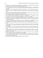
GND GND GNDVDD VDD
M1 metal
M2 metal
Footer locations
VGND
VGND
VGND
VDD
VDD
VDD
FIGURE 39.14 Coarse-grained power gating with macro/core. GND =Ground; VDD =voltage drain drain;
VGND =virtual ground.
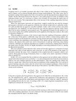
Fine-grained power gating, as shown in Figure 39.15, where the footer switches are implemented
withinthe logic in a regularlayoutare moredesirable in a high-performancedesign wherethe voltage
drop across the power gate as well as IR and EM (electromigration) requirements are more stringent.
39.7 INTO THE FUTURE
We have summarized the current workings of IBM’s physical synthesis capabilities to display the
complexities of such a system. Physical synthesis requires a seamless integration of many previously
separatedesign automationdomains, suchasoptimization,placement,timing,extraction, androuting.
However, as technology progresses toward 45 nm and beyond, more will be demanded of physical
synthesis. It must be dynamic and must constantly adapt to changing technologies, design styles,
and design specifications.
Timing closure will continue to evolve into the even more complex problem of design closure.
Design closure requires that accurate modeling o f the clock tree network and routing be incorporated
earlier and earlier up the physical synthesis pipeline to take into account their effects on timing and
signal integrity. Meeting global power constraints, using multithreshold voltages, voltage islands,
power gating,etc. also becomes morecritical. One must pay attention to how physical-designchoices
relate to chip fabrication, so design fo r manufacturability and handlin g of variability will become
increasingly important. Optimizations must become more sophisticated to take these additional
objectives into account.
Increasing chip sizes and additional requirements for physical synthesis to meet and incorporate
these additional constraints also further exacerbates the ability to run efficiently, perhaps an other
reason why hierarchical design is becoming more prevalent.
GND
VGND
Virtual
grid
Macro/core
M2 metal
M1 metal
Footer switch
location
Global
grid
FIGURE 39.15 Fine-grained power gating within a block. GND=Ground and VGND =virtual ground.
Alpert/Handbook of Algorithms for Physical Design Automation AU7242_C039 Finals Page 833 29-9-2008 #22
Placement-Driven Synthesis Design Closure Tool 833
REFERENCES
1. C. J. Alpert, C. -N. Chu, and P. G. Villarrubia. The coming of age of physical synthesis, In IEEE/ACM
ICCAD, San Jose, CA, 2007, pp. 246–249.
2. L. Trevillyan, D. Kung, R. Puri, L. N. Reddy, and M. A. Kazda. An integrated environment for technology
closure of deep-submicron IC designs. In IEEE Design and Test of Computers, pp. 14–22, January 2004;
W. Donath, P. Kudva, L. Stok, P. Villarubia, L. Reddy, A. S ullivan, Transformational placement and
synthesis, in Proceedings of the Conference on Design, Automation and Test in Europe Exhibition,Paris,
France, 2000, pp. 194–201.
3. C. J. Alpert, S. K. Karandikar, Z. Li, G. -J. Nam, S. T. Quay, H. Ren, C. N. Sze, P. G. Villarrubia, and M.
C. Yildiz. Techniques for fast physical synthesis. Proceedings of the IEEE, 95(3):573–599, March 2007.
4. U. Brenner and A. Rohe. An effective congestion driven placement framework. In P roceedings of
International Symposium on Physical Design, San Jose, CA, pp. 6–11, 2002.
5. J. Darringer, E. Davidson, D. J. Hathaway, B. Koenemann, M. Lavin, J. K. Morrell, K. Rahmat, W. Roesner,
E. Schanzenbach, G. Tellez, and L. Trevillyan. EDA in IBM: Past, present, and future. IEEE Transactions
on Computer-Aided Design of Integr ated Circuits and Systems, 19(12):1476–1497, December 2000.
6. I. Sutherland, R. F. Sproull, and D. Harris. Logical Effort: Designing Fast CMOS Circuits. Morgan
Kaufmann, San Fransisco, CA, 1999.
7. L. Trevillyan, P. Kotecha, A. Drumm, and R. Puri. A Method for Incremental Cell Placement for Minimum
W ire Length, U. S. patent pending.
8. E. Bozorgzadeh, S. Ghiasi, and M. Sarrafzadeh. Optimal integer delay budget assignment ondirected acyclic
graphs. IEEE Transactions on CAD of ICs and Systems, 23(8):1184–1199.
9. V. Kravets and P. Kudva. Implicit enumeration of structural changes in circuit optimization. I n Proceedings
of Design Aut omation Conference, San Diego, C A, pp. 439–441, June 2004.
10. R. E. Bryant. Graph-based algorithms for Boolean function maniupulation. IEEE Transactions on
Computers, C-35(6):677–691, August 1986.
11. G. R. Chiu, D. P. Singh, V. Manohararajah, and S. D. Brown. Mapping arbitrary login functions into
synchronous embedded memories for area reduction on FPGAS. In IEEE/ACM ICCAD, San Jose, CA,
pp. 135–142, 2006.
12. B. Guan and C. Sechen. Large standard cell libraries and their impact on layout area and circuit performance.
In IEEE ICCD, Austin, TX, pp. 378–383, 1996.
13. A. Hussain and K. Umino. Method to close timing on a ll corners with synopsys galaxy at and below
130 nm. In SNUG, San Jose, CA, 2005.
14. R. Murgai. Improved l ayout-driven area-constrained timing optimization by net buffering, In 18th Interna-
tional Conference on VLSI Design held jointly with 4th International Confer ence on Embedded Systems
Design (VLSID’05), Kolkota, India, pp. 97–102, 2005.
15. V. N. Kravets. Constructive multi-level synthesis by way of functional properties. PhD Thesis, University
of Michigan, Ann A rbor, MI, 2001.
16. C.Guardiani,M.Bertoletti, N. Dragone, M. Malcotti, and P. McNamara. An effectiveDFM strategy requires
accurate process and IP pre-characterization. In IEEE/ACM DAC, Anaheim, CA, pp. 760–761, June 2005.
17. H. Ren, D. Z. Pan, C. J. Alpert, and P. Villarrubia. Diffusion-based placement migration. In Proceedings of
Design Automation C onference, Anaheim, CA, pp. 515–520, 2005.
18. R. Puri, L. Stok, J. Cohn, D. Kung, D. Pan, D. Sylvester, A. Srivastav a, and S. Kulkarni. Pushing ASIC
performance in a power envelope. In Proceedings of Design Automation Conference, Anaheim, C A, p. 788,
2003.
19. H. Li, S. Bhunia, Y. Chen, T. N. Vijaykumar , and K. Roy. Deterministic clock gating for microprocessor
power reduction. In High-Performance Computer Architecture, Anaheim, CA, pp. 113–122, 2003.
Alpert/Handbook of Algorithms for Physical Design Automation AU7242_C039 Finals Page 834 29-9-2008 #23
Alpert/Handbook of Algorithms for Physical Design Automation AU7242_C040 Finals Page 835 29-9-2008 #2
40
X Architecture Place
and Route: Physical Design
for the X Interconnect
Architecture
Steve Teig, Asmus Hetzel, Joseph Ganley,
Jon Frankle, and Aki Fujimura
CONTENTS
40.1 Introduction 835
40.2 History 836
40.3 X InterconnectArchitecture 836
40.4 Theoretical Benefits of X 837
40.5 Limitations of X 839
40.6 Role of Vias 840
40.7 System ForX Place and Route 840
40.8 X Placement 840
40.9 X Global Routing 843
40.10 X Detailed Routing 848
40.10.1 Routing Space Model and Search Algorithm 849
40.10.2 Manufacturing-Constrained Routing 851
40.11 X Steiner Trees 855
40.12 X Manufacturing Considerations 856
40.13 X in Practice 859
40.14 Summary 860
References 861
40.1 INTRODUCTION
For 40 years, physical design dogma has decreed that (nearly) every wire on a chip b e Manhattan—
either horizontal or vertical—despite the intuition that adding diagonal wires should significantly
reduce the total interconnect required to implement a design. This chapter briefly provides some
historical context for the ubiquity of Manhattan wiring and then introduces and explores the
X interconnect architecture [IML+02,T02], which combines diagonal and Manhattan wires per-
vasively to improve IC layout. Realizing the theoretical benefits of X, which are substantial and
surprisingly diverse, in practice has proven to be quite challenging, demanding both a careful reex-
amination and refinement of the manufacturing flow and a material revision of almost every tool in
the physical design flow. For example, X place and route (XPR)—the X system described here—has
required new methods for floorplanning, wire load estimation in synthesis, global placement, global
835
Alpert/Handbook of Algorithms for Physical Design Automation AU7242_C040 Finals Page 836 29-9-2008 #3
836 Handbook of Algorithms for Physical Design Automation
routing, detailed placement, detailed routing, parasitic extraction,OPC, clock routing, power routing,
geometric search, and even database representation. The novelty of these methods has resulted in
numerous patents. Even as X has begun to see commercial use, with X chips from Toshiba and ATI,
among others, many challenges remain, and X-enabled physical design techniques should become
and increasingly active area of research in both academia and industry in the coming years.
40.2 HISTORY
The transistors for almost every chip are distributed across the chip’s two-dimensional surface, so
at least two routing directions are required for the flexible interconnection of those transistors. Until
the mid-1980s, it was not practical to have more than one or two layers of metal wiring above the
polysilicon, or poly, layer. Because chips are generally rectangular so that the silicon wafers on
which they are manufactured can be efficiently diced, it seemed logical to make the poly layer and
the one metal layer (M1) orthogonal and axis-parallel.
∗
The second metal layer, M2, where it was
used, was typically orthogonal to M1. Very short diagonal jogs were used in some channel routers
and to miter the corners in the power rail through the I/O pads, but general diagonal wiring was
not seriously considered. With the introduction in the late 1980s of planarization techniques to IC
manufacturing, an additional layer of metal, M3, b ecame widely available, which single-handedly
precipitated the invention of modern,area-based, place-and-routemethods and their rapid dominance
over the row-and-channel-basedtechniques that preceded them. Although hexagonal wiring (i.e., 0
◦
,
120
◦
, and 240
◦
)—now, sometimes called the Y architecture [CCK+03]—could, in principle, have
been very powerful even then, the newness of multilayer, Manhattan IC manufacturing caused th e
fabs to fear the added complexity of adding diagonal wires as well. So, despite a few theoretical papers
(e.g., [K95] and referencestherein)andpatents [FHM+98,SKK+96](never reduced to practice)in the
mid-1990s,there was no significant,practical exploration of diagonalwiring, either in manufacturing
or in EDA, before the X effort at Simplex Solutions in the 1990s. Fortunately, the number of wiring
layers increased sharply in the 1990s, which motivated a reexamination of the possible benefits of
diagonal wiring and the practical hurdles involved in realizing them.
There are two apparent challenges in producing chips with diagonal wires: manufacturing and
EDA. As it happens, for some diagonal interconnect architectures, such as those that add 45
◦
and
135
◦
wires to Manhattan wires, mainstream manufacturing flows and equipment enable reasonably
straightforward fabrication. Physical design for diagonal wiring, on the other hand, is considerably
more challenging thanit first appears,andXPR—the first full-fledged suchphysical designsystem—
required dozens of person-years of development before reaching industrial-strength maturity.
The sections that follow describe the X interconnect architecture, which u ses both Manhattan
and d iagonal wires pervasively,and introduce some of the many EDA innovationsthat were required
to reduce X to practice.
40.3 X INTERCONNECT ARCHITECTURE
Moore’s law has been largely driven by the regularity and rapidity with which fabs have been
able to shrink transistors and wires while still manufacturing them reliably. Even with the 20-fold
shrink from the 5-µ (∼1982) to the 0.25-µ (∼1982) technology node, transistors continued to
dominate area, performance, and power. But the emergence of nanometer technologies (e.g,. 180,
130, 90 nm, etc.) starting in the late 1990s so sharply increased the relative impact of wires versus
transistors on area, performance, and power as to necessitate radical innovations in the interconnect.
The severity of the interconnect problem at nanometer nodes is evident from the replacement of
aluminum wires on chips with copper: a multibillion-dollar effort that required new chemistry, new
∗
In fact, even in the two-layer case, the total wirelength would be reduced by about 1 percent by making the two wiring
directions be northeast a nd northwest instead, but the complexity of doing so outweighs a mere 1 percent benefit.
Alpert/Handbook of Algorithms for Physical Design Automation AU7242_C040 Finals Page 837 29-9-2008 #4
X Architecture Place and Route: Physical Design for the X Interconnect Architecture 837
equipment, and revised EDA tools that collectively reduced interconnect delay by ∼50 percent. Of
course, changes of wiring material are not the only tools available, and other radical suggestions,
such as the pervasive use of diagonal wires, reemerged as worthy of consideration. Just as with
the introduction o f copper wiring, though, the benefits of diagonal wires carry significant practical
challenges with them.
For one, most of the equipment for the generation of masks and the manufacture of chips relies
on an underlying, fine, discrete grid. All manufactured structures must have their edges on this grid,
which was designed for Manhattan wiring but also directly permits 45
◦
(northeast or NE) and 135
◦
(northwest or NW), because a diagonal wire of length k
√
2, where k is a positive integer, resolves
into k units in each of the horizontal and vertical directions. The apparent manufacturability of NE
and NW wires suggested that an interconnect architecture with Manhattan, NE, and NW wires could
provide the benefits of diagonals in a practical implementation. By contrast, the griddedness of
manufacturing is a significant obstacle to the practicality of hexagonal wiring, for example, as the
edges of the wires do not lie on grid. Further, at least one of the legs of a 30–60–90 right triangle
must be irrational; that is the
√
3 term does not cancel for h exagonal wiring the way that the
√
2
terms do for the X architecture.
A second consideration is that lower layers of wr iting (e.g., M1 and M2 ) are typically used for
the internal connections of the standard cells and IP blocks themselves. Because cells and blocks
are overwhelmingly Manhattan, there was no significant benefit in adding diagonals to those wiring
layers for connections between cells. On the other hand, upper layers of mental are specifically
intended for connections between cells, so it is more reasonable to combine Manhattan and diagonal
wires there.
An X interconnect architecture is one that combines the extensive use of both Manhattan wires
and d iagonal wires. In practice, distinct wiring layers (or, at least, regions within those wiring layers)
are devoted to particular Manhattan o r diagonal preferred directions. While one can construct an
X architecture with each layer having wires rotated 45
◦
with respect to the previous layer, it is
improbable that such structures outperform those in which layers are stacked in orthogonal pairs.
Further, the desire for backward compatibility with Manhattan-b ased infrastructure, such as standard
cell libraries, has strongly influenced the application of diagonals in practice.
The above observations—particu lar ly, backward compatibility—motivated th e typical use in
practice of X inter c onnect architectures in which M1–M3 are Manhattan, typically alternating
between horizontal and vertical preferred directions on successive layers, M4 is diagonal (e.g.,
NE), and M5 is perpendicular to M4 (e.g., NW). If there are additional metal layers, such as M6 and
M7, they are again Manhattan, while M8 and M9 could be diagonal. Thus,
1. Every layer is adjacent to a perpend icular layer (to facilitate efficient local wiring)
2. Every sequential quartet of layers above M1 contains a horizontal, a vertical, a NE, and
a NW (to facilitate efficient, larger-scale wiring)
An interconnect architecture that satisfies these two properties makes the name “X” apparent,
owing to the novel, X-shaped intersection of adjacent d iagonal layers. However, the term and the
techniques described in this chapter apply more generally to any interconnect architecture in which
both Manhattan and diagonal wires play a significant role.
40.4 THEORETICAL BENEFITS OF X
X, both in theory and in practice, reduces chip area, wirelength, delay, coupling capacitance, and
power versus Manhattan, sometimes to such as extent that a full layer of interconnect can be
removed. To estimate these benefits analytically, it is easiest to begin with wirelength reduction.
Most current placement algorithms minimize some approximation to the sum over all nets of the
Alpert/Handbook of Algorithms for Physical Design Automation AU7242_C040 Finals Page 838 29-9-2008 #5
838 Handbook of Algorithms for Physical Design Automation
semiperimeter of each net’s Manhattan bounding box.
∗
As a result, placers optimize a correlate to
wirelength, possibly weighted by timing considerations or congestion, but one might expect that
they are unbiased with respect to bounding-box aspect ratios. To test this hypothesis, we examined
dozens of industrial, Manhattan designs early in the X project and found that, in fact, aspect ratios
are distr ibuted uniformly.
At least 55–60 percent of nets in contemporary designs are two-pin nets even before placement,
and the increasing use of buffers has sharply increased that percentage after placement. So, as a
simple but reasonable estimate of the wirelength reduction versus Manhattan to expect with X,
one can estimate the expected reduction in the wirelength of a two-pin net with a random aspect
ratio. In the Manha ttan metric, a c ircle (i.e., th e locus of points at a fixed distance from a specified
center point) is diamond-shaped; for the X metric, the circle is octagonal. Consider a connection with
extent (|x|, |y|). Without lossof generality,supposethat (|x|≥|y|); then, the Manhattan-to-X
wirelength reduction for this connection is 1−[|x|+|y|(
√
2 −1)]/(|x|+|y|). The expected
value of this reduction, assuming that the source is at the center of a diamond, and the sink’s location
is uniformly distributed around the periphery is Ref. [T02].
1 −
1/2
0
√
2 −2
y +1
dy
1/2
0
dy
∼
=
14.6 percent
Importantly, this analysis assumes that only the router has changed, yet the real benefits of X become
apparent only by making the whole system X-aware. For example, suppose that the placer is X-aware
too; then, by analogy to the Manhattan system, the placer for X minimizes wirelength but is unbiased
with respect to aspect ratio. To model an X placer analytically, rearrange the components that would
have been placed within the Manhattan disk of radius r (i.e., filled diamond) to occupy an X d isk
(i.e., filled octagon) of equal area [T02]. The resulting wirelen gth reduction, which is one minus the
ratio the octagon’s radius of a diamond of equal area, is 1 − (1/2)
1/4
∼
=
15.9 percent.
†
For the significant fraction of high-end designs that are core-limited rather than pad-limited,
substantial additional improvement with X is possible, though. Most designs have utilizations far
below 100 percent: often as low as 70 percent or even lower for interconnect-dominated designs,
such as network switches [BR02]. It is reasonable to assume that X-place-and-route systems are as
good at optimizing X objective functions as Manhattan place-and-route systems are at optimizing
Manhattan objectives, but reducing wirelength by 15.9 percent while leaving die size unchanged
would leave the X router with a much easier problem than a Manhattan router had. Instead, an X
system can exploit the wirelength reduction versusManhattan by shrinkingthe die until the X routing
is as dense as the Manhattan routing was in the o riginal design. In particular, reducing wirelength
by 15.9 percent would require a die size shrink of 15.9 percent to restore the wiring density of the
original Manhattan layout. Of course, this die size reduction would permit an additional wirelength
reduction of 1 −[1 −(1 /2)
1/4
]
1/2
∼
=
8.3 percent, which, in turn, permits an additional die shrink of
8.3 percent, etc. The resulting infinite product converges to a wirelength and die size reduction of
(1−1
√
2)
∼
=
29.3 percent. This reasoning demonstrates that, in general, any technique that achieves
a wirelength reduction of R percent with fixed area can be used to achieve a wirelength reduction
∗
Of course, the minimization of bounding-box semiperimeters, despite its near-ubiquity in current placers, ignores the
location of pins within the box and the concomitant flexibility of wiring; it is, thus, a very crude measure of placement
quality.
†
The analogous analysis for Euclidean (i.e., all-angle) wiring results in a wirelength reducton of 1 −
√
(2/π)
∼
=
20.2 percent
versus Manhattan.
Alpert/Handbook of Algorithms for Physical Design Automation AU7242_C040 Finals Page 839 29-9-2008 #6
X Architecture Place and Route: Physical Design for the X Interconnect Architecture 839
of almost 2R percent (i.e., R(2 −R) percent) if area reduction is used to maintain constant layout
difficulty. Particularly for wire-dominated designs such as networking chips, which typically have
low utilizations with Manhattan wiring, significant die size reduction is possible with X. Although
the above analysis is somewhat aggressive in assuming that all nets have only two pins, it is also
conservative in that the substantial add itional area reduction owing to the concomitant shrinkage of
driversand elimination of buffersisnotconsidered. In practice,reducing thediesize by 15–20percent
and the wirelength by 20–25 percent has proved straightforward in general, and the alternative of
not reducing the die size but instead using X to remove a wiring layer (e.g., at ATi)—and sometimes
two wiring layers—has also been achieved.
One additional, nonobvious, benefit of X is its utility for routing over IP blocks. Most IP blocks
(e.g., memories) use Manhattan wiring for layers 1–3 and sometimes 4, and many have the restriction
that Manhattan wiring over the block is forbidden due to capacitive coupling considerations. X, on
the other hand, can cross over such such blocks diagonally with no risk of parallel runs between the
over-the-block wiring and within-the-block wiring. Because more than half of a typical chip today
is occupied by IP such as memory blocks, the opportunity to use the entirety of the upper wiring
layers confers substantial benefit.
40.5 LIMITATIONS OF X
Although both practical experience with X and theoretical analysis demonstrate its significant
benefits—to wirelength, area, delay, power, etc.—X is not a panacea. For example, the above analy-
sis demonstrates that the wirelength reductio n is nearly doubled by permitting area reduction, but
for those atyp ical desig ns that have extremely high utilizations (e.g ., more than 90 percent of the
die is occupied by components that are not buffers), X can provide only more modest wirelength
reductions. Clearly, for blocks that have highly eccentric aspect ratios ( e.g., 5:1), the u se of diagonals
does not buy much. In practice, such narrow blocks typically abut Manhattan IP blocks, though,
so over-the-IP, diagonal wiring somewhat mitigates the diminished utility of X within the eccentric
block.
X requires enough wiring layers for some of them to be used for diagonals; for low-end devices
for which signal routing extends only to M4, for example, X cannot be usefully applied. Finally,
for designs with extensive Manhattan constraints on the upper wiring layers, diagonal wiring can be
difficult to incorporate effectively. For example, if the floorplan is Manhattan-oriented, so that large
horizontal buses cross an X block on M4, large-scale, diagonal wires on M4 become infeasible by
construction.
In practice, though,the vastmajority ofdesigns showsignificantwirelength anddie size reduction
with X when compared to their Manhattan equivalents. Curiously, the most significant limitation of
X in practice is the widespread misconception that X changes only the router and not the full layout
system. Indeed, as the theoretical analysis above shows, keeping the area and the placement fixed
and changing only the wiring to permit diagonals buys only 14.6 percent wirelength reduction and
achieves that only for netlists with only two-pin nets. For real netlists, the improvement is somewhat
lower in practice—perhaps, 10 percent (e.g., [I06])—if only the wiring is perm itted to change. Using
a Manhattan floorplan, and Manhattan buses on the upper layers, can make the situation even worse.
To see the benefits of X in practice, one must apply it to problems it addresses well:
• Designs for which high utilization could not be achieved in Manhattan
• Designs that are not overly eccentric in aspect ratio
• Designs with enough wiring layers to devote part of at least one to diagonals
• Designs that accommodate X by not overconstraining the upper layers with required
Manhattan wires, and, most importantly
• Designs that permit the whole layout system, and just the router, to be X-aware
Alpert/Handbook of Algorithms for Physical Design Automation AU7242_C040 Finals Page 840 29-9-2008 #7
840 Handbook of Algorithms for Physical Design Automation
40.6 ROLE OF VIAS
Analyses such as the one above assume that vias between layers are free. Although the interconnect
delay caused by vias is sharply reduced with copper wires, vias remain the most difficult features to
manufacturereliably on an integrated circuit, and reducing the number of vias can have a significant,
positive effect on yield. In addition, vias create routing obstacles on two layers, rather than one, so
reducing the number of vias can significantly simplify layout.
An even more entrenched dogma than the use of Manhattan wiring is the use of preferred-
direction wiring: that is, the requirement that each routing layer have a designated, preferred wiring
direction (e.g., horizontal), such that virtually all of the wire length on that layer is required to be in
the preferred direction. The assumption of a preferred direction for each layer significantly simplifies
and accelerates routing algorithms, but it also demands a via for every change of direction and, thus,
for any connection in a Manhattan layout that is not exactly vertical or horizontal. Because X can
move diagonally without using a via, it has the potential to reduce the number of vias significantly.
On the other hand, backward compatibility with existing, Manh attan cell libraries demands that the
diagonal layers are upper layers (e.g., M4 and M5), so extra vias are required to use the diagonals,
mitigating via reduction somewhat. The p ronounced impact of vias on the both yield and layout thus
motivates the consideration of nonpreferred-direction wiring: layouts in which wires in multiple
orientations coexist on the same wiring layer.
Even a conservative nonpreferred-direction strategy for X, using d iagonal jogs on Manhattan
layers and Manhattan jogs on diagonal layers, can sharply reduce the number of vias required for
layout, and XPR sees substantial via reductionsin practice versus contemporary Manhattan systems.
More radical than short, nonpreferred-direction jogs, though, but considerably more powerful is
the complete abandonment of the preferred-direction requirement. Full directional freedom on all
layers, called liquid routing, makes the fullest use of the power introduced by diagonals, but is far
more challenging from an EDA point of view than preferred-direction X. In the addition, the yield
benefits of a via reduction from liquid routing must be weighed against lithographic concerns about
nonpreferred-direction wiring in nanometer technologies to assess its long-term practicality. From
an academic point of view, though, liquid routing is almost completely unexplored territory. The
problems there are particularly challenging, but the potential, practical payoff is high. The reader
is encouraged to investigate the patents by Caldwell and Teig on Q
∗
and related liquid routing
ideas [TC04,TC05,TC06] as a starting point for future work.
40.7 SYSTEM FOR X PLACE AND ROUTE
In the sections that follow, we describe a few of the tools and techniques used within XPR that
made X layout possible starting in 2001. Many additional X-aware tools are required, ranging from
parasitic extraction to clock routing and even to visualization infrastructure, as quad and K-D trees
(Section 4.3.2) are highly inefficient for region queries with both long diagonal and long Manhattan
wires. We confine the presentation here to placement, global routing, detailed routing, and Steiner
tree construction.
40.8 X PLACEMENT
Placement is typically performed in one of the three ways: recu rsive partitioning, analytical tech-
niques, or Monte Carlo methods such as simulated annealing. Annealing, which is often used for
detailed placement but rarely for global placement anymore because of its high computational
expense,can bedirectlyadapted to theXinterconnectarchitecture bychanging the objectivefunction,
but the other two placement methods require much more drastic modifications.
Alpert/Handbook of Algorithms for Physical Design Automation AU7242_C040 Finals Page 841 29-9-2008 #8
X Architecture Place and Route: Physical Design for the X Interconnect Architecture 841
Another commo n approach to mod ern placement is analytical formulation. Here, th e netlist’s
wirelength is approximated by a continuously differentiable function that is either directly mini-
mized with a conjugate gradient-based minimizer (or other derivative-basedtechniques) or indirectly
minimized using a linear system of equations whose solution minimizes the original wirelength
formula.
An unusual and significant challenge in X placement stems from the inseparability of two-
dimensional distance into independent, one-dimensional components. The Manhattan distance
between (x1, y1) and (x2, y2) is simply |x2 − x1|+|y2 − y1|,sox and y can be treated indepen-
dently, and reducing distance by one unit in either x or y is equally desirable, all other considerations
(e.g., congestion) being equal. Distance in X, though, is max (|x2 − x1|, |y2 − y1|) + (
√
2 − 1)
∗
min(|x2 − x1|, |y2 − y1|). When this equation is differentiated, the resulting derivative inter-
twines x and y in ways for which most analytical placers and partitioners were not designed. In
fact, this requirement for separability is why most an alytical placers use either squared Euclidean
length [KSJA91], some approximation of linear wirelength using piecewise squared length [SDJ91]
or β-regularization [BKKM01], or some other approximation such as bounding-box semiperimeter
[KRW05]. All of these techniques have the desirable property that the x-andy- equations are sparse
and separable: that is, can be solved as two separate systems, thus greatly reducing runtime.
Typical analytical placement techniques often also requ ire separability within the legalization
step that follows, which is usually partitioning-based. For example, it is no t clear that techniques
such as Ref. [V97] can be made X-aware, even in principle.
Methods such as β-regularization [BKKM01] and conjugate gradient methods [KRW05] can be
generalized to accommodate X, at the expense of some implementation complexity, and this would
be a potentially fruitful area for future research.
By contrast, recursive partitioning methods, either standalone or as legalization methods for
analytical placers, seem to be fundamentally incompatible with X. To see this, consider how a
modern partitioning algorithm works. Mo st of these techniques are ultimately derived from the early
algorithm of Kernighan and Lin [KL70], later improved by Fiducia and Mattheyses [FM82]. After
the authors’ names, this type of approach is typically referred to as KLFM.
The KLFM algorithm first divides the set of components into two roughly equal-sized subsets.
It then moves or swaps individual components between these subsets heuristically to minimize the
number of nets that contain components in both subsets—that is, that are cut. The KLFM algorithm
itself is a fairly simple local optimization heuristic, yet it performs quite well on this problem.
An enormous amount of later research builds improvements onto the basic KLFM structure (see
Section 7.2).
The way that KLFM is typically used to solve the placement problem is by recursive bip artition-
ing, in which the two-dimensional placement problem is artificially decomposed into a sequence of
one-dimensio nal partitioning problems. This is accomplished by specifying a vertical or horizon tal
cutline that roughly bisects the placement area and using KLFM to partition the set of components
into two subsets that are constrained to lie on opposite sides of the cutline. Then, each partition is,
in turn, bisected by a cutline, and KLFM divides the subset within the partition into two smaller
subsets that are constrained to lie on opposite sides o f the partition’s cutline. This process contin-
ues recursively until only a few components are left in each partition. A variety of techniques have
been devised for terminal propagation, which allows the algorithm to capture the influence of con-
nected components outside of th e current subproblem on the p lacement of the components inside
the subproblem to which they are connected.
Unfortunately,recursivebipartitioningof this type is poorly suited to the X interconnect architec-
ture. The use of horizontal and vertical cutlines one at a time assumes the separability of horizontal
and vertical distances in assessing placement quality just as many of the analytical placement tech-
niques do. The inseparability of the X metric means that even the addition of diagonal cutlines to
a partitioning strategy will not capture X p lacement quality, which depends fundamentally on the