- Trang chủ >>
- Khoa Học Tự Nhiên >>
- Vật lý
Handbook of algorithms for physical design automation part 102 doc
Bạn đang xem bản rút gọn của tài liệu. Xem và tải ngay bản đầy đủ của tài liệu tại đây (217.66 KB, 10 trang )
Alpert/Handbook of Algorithms for Physical Design Automation AU7242_C047 Finals Page 992 10-10-2008 #9
992 Handbook of Algorithms for Physical Design Automation
a mincost maxflow problem, which has the form of a transportation problem. The flow graph is
constructed as follows:
• Source node of the flow graph is connected through directed edges to a set of nodes v
i
,
representing candidate thermal vias; the edges have capacity 1 and cost 0.
• Directed edges connect a second set of nodes, T
j
, from each tile to the sink node, with
capacity equalin g the number of vias that the tile can contain, and cost zero. The capacity
is computed using a heuristic approach that takes into account the temperature difference
between the tile and the one directly in the tier below it (under the assumption that heat flows
downward toward the sink); the thermal analysis is based on a commercial FEA solver.
• Source and sink both have cost m, which equals the number of intertier vias in the entire
region.
• Finally, a node v
i
is co nnected to a tile T
j
through an arc with infinite capacity and cost
equaling the estimated wirelength of assigning an intertier via v
i
to tile T
j
.
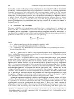
Another approach to 3D routing, presented in Ref. [17], combines the problem of 3D routing
with heat removal by inserting th e rmal vias in the z direction, and introduces the concept of thermal
wires. Like a thermal via, a thermal wire is a dummy object: it has no electrical function, but is used
to spread heat in the lateral direction. Each tier is tiled into a set of regions, as shown in Figure 47.6.
The global routing scheme goes through two phases. In phase I, an initial routing solution is
constructed. A 3D MST is built for each multipin net, and based on the corresponding two-pin
decomposition, the routing congestion is statistically estimated over each lateral routing edge using
the method in Ref. [18]. This congestion model is extended to 3D by assuming that a two-pin net
with pins on different tiers has an equal probability of utilizing any intertier via position within the
bounding box defined by the pins.
A recursive bipartitioning scheme is then used to assign intertier vias. This is also formulated
as a transportatio n problem, but the formulation is different from the multilevel method described
above. Signal intertier via assign ment is then performed across the cut in each recursive b ipartition.
Grid cell at
the corner
Routing grid
Routing graph
Vertex in
routing graph
Vertical
routing edge
Grid cell
boundary
FIGURE 47.6 Routing grid and routing graph for a four-tier 3D circuit. (From Zhang, T., et al., In Proceedings
of the Asia-South Pacific Design Automation Confer ence, 2006. Copyright IEEE. With permission.)
Alpert/Handbook of Algorithms for Physical Design Automation AU7242_C047 Finals Page 993 10-10-2008 #10
Physical Design for Three-Dimensional Circuits 993
(a) (b)
Assign
signal
vias
first
Assign
signal vias
after
higher-level
assignment
Layer 0
Layer 1
Layer 2
Layer 3
Group 0
Group 1
(Capacity, cost) pair
N1
N0
N4
N 3
N 2
C 0
C3
C2
C1
S
T
(1, 0)
(1, cost (N
i
, C
j
))
(U
j
, 0)
FIGURE 47.7 (a) Example of hierarchical signal via assignment for a four-tier circuit. (b) Example of min-
cost network flow heuristics to s olve signal via assignment problem at each level of hierarchy. (From Zhang,
T.,etal.,InProceedings of the Asia-South Pacific Design Automation Conference, 2006. Copyright IEEE. With
permission.)
Figure 47.7a shows an example of signal intertier via assignment for a decomposed two-pin signal
net in a four-tier circuit with two levels of h ierarchy. The signal intertier via assignment is first
performed at the boundary of group 0 and group 1 at topmost level, and then it is processed for
tier boundary within each group. At each level of the hierarchy, the problem of signal intertier via
assignment is formulated as a min-cost network flow.
Figure 47.7b shows the network flow graph for assigning signal intertier v ias of five intertier nets
to four possible intertier via positions. The idea is to assign each net that crosses the cut to an intertier
via. Each intertier net is represented by a node N
i
in the network flow graph; each possible intertier
via position is indicated by a node C
j
.IfC
j
is within the bounding box of the two-pin intertier net
N
i
, we build a directed edge from N
i
to C
j
, and set the capacity to be 1, the cost of the edge to be
cost(N
i
, C
j
).Thecost(N
i
, C
j
) is evaluated as the shortest path cost for assigning intertier via position
C
j
to net N
i
when both pins of N
i
are on the two neighboring tiers; otherwise it is evaluated as the
average shortest path cost over all possible unassigned signal intertier via positions in lower levels
of the hierarchy. The shortest path cost is obtained with Dijkstra’s algorithm in the 2D congestion
map generated from the previous estimation step, and the cost function for crossing a lateral routing
edge is a combination of edge length and an overflow cost function similar to that in Ref. [19]. The
supply at the source, equaling the demand at the sinks, is N, the number of nets.
Finally, once the intertier vias are fixed, the problem reduces to a 2D routing problem in each
tier, and maze routing is used to route the design.
Next, in phase II, a linear programming approach is used to assign thermal vias and thermal wires.
A thermal analysis is performed , and fast sensitivity analysis using the adjoint network method, which
has the cost of a single thermal simulation. The benefit of adding thermal vias, for relatively small
perturbations in the via density, is given by a product of the sensitivity and the via density, a linear
function. The objective function is a sum of via d ensities and is also linear. Additiona l constraints are
added in the formulation to permit overflows, and a sequence of linear programs is solved to arrive
at the solution.
47.3 3D FPGA DESIGNS
As in the case of standard cell designs, the idea of building 3D designs using FPGAs is not new,
and there has been some earlier work in this area. Alexander et al. [20] proposed using the MCM
(multichip module) technology with through die v ias to build 3D FPGAs, and enumerated a number
of issuesthat should be considered inbuilding3D FPGAssuch asyield,channelwidth,thermalissues,
Alpert/Handbook of Algorithms for Physical Design Automation AU7242_C047 Finals Page 994 10-10-2008 #11
994 Handbook of Algorithms for Physical Design Automation
and placement and routing. A 3D FPGA architecture called Rothko, in which each RLB (routing and
logic block) tile is connected to the RLB directly above and below it (i.e., no multilength segments
in the z direction), was presented in Ref. [21]. The process technology that the authors assumed was
that of Northeastern University’s 3D fabrication technology, which was similar to that of MIT’s [4].
A more advanced version of Rothko’s work appears in Ref. [22] in which the authors propose
placing the routing in one lay e r and logic on another for more efficient layer utilization. Other
notable contributions include the work by Lin et al. [23] and Chiricescu et al. [24], who propose
placing memory and routing elements functions in different tiers; Campenhout et al. [25], who
proposes using optical interconnects to provide communications between tiers of a 3D FPGA; and
Wu et al. [26], who propose a universal switchbox for 3D FPGAs.
Recent 3 D FPGA CAD efforts can be classified into estimation m ethods and placement and
routing algorithms. In the estimation methods, analytical models are developed to estimate 3D
wirelength and channel width, and as a result estimating the power consumption and area of a 3D
FPGA design. Because such methods do not require costly placement and routing steps, they can
predict resourcerequirementsvery fastatthecostofestimation accuracy. Inthe placement androuting
methods, specialized CAD algorithms are developed to target specific needs of a 3D architecture.
In the following sections we discuss both categories: estimation and placement/routing.
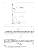
47.3.1 ESTIMATION METHODS
Analytical models for estimating channel width in gate arrays were studied by Gamal [27]. He
observed that the channel width follows a Poisson distribution and the average channel width W is
estimated as
W =
γ L
2
(47.3)
where
γ is the average number of edges incident to logic blocks
L is the average wirelength
Later studies have shown that better estimations can be obtained by considering multiterminal
nets and their wirelength distributions. Rahman et al. [28] extend these models for a 2D FPGA with
unit routing segments as follows:
W =
2
√
N−2
l=1
lf (l)X
fpgn
2Ne
t
(47.4)
where
N is the number of CLBs (configurable logic block, or the basic unit of the FPGA logic)
l is the wirelength
f (l) is the probability density function of the wirelength and can be derived from the Rent’s rule
Parameters X
fpga
and e
t
are architecture and placement and routing dependent. X
fpga
is a multi- to two-
terminal routing adjustment factor and e
t
is the channel utilization factor. Typically 5–10 percent
of the routing segments are shared among multiple terminals of a multiterminal net, resulting in
X
fpga
= 90–95 percent. Channel utilization e
t
is less than one because of detours in the routing.
For a 3D FPGA, they assume F
s
= 5 for every switch (where F
s
is as defined in Section 45.4.3.)
where N
z
is the number of 3D tiers. The maximum length in the third dimension is (N
z
−1)t
z
where
Alpert/Handbook of Algorithms for Physical Design Automation AU7242_C047 Finals Page 995 10-10-2008 #12
Physical Design for Three-Dimensional Circuits 995
t
z
is the distance between adjacent tiers. The average channel width in a 3D FPGA is estimated as
the following:
W =
2
√
N/N
z
−2+(N
z
−1)t
z
l=1
lf
3D
(
l
)
X
fpga
2N +
(
N
z
−1
)
N
N
z
e
t
(47.5)
where f
3D
(l) is the 3D wirelength distribution function.
The analytical model for channel width estimation is further improved in Ref. [29] by factoring
in the under-utilizationof the CLBs, which changes the number of nets by a factorof u
p+1
and the chip
area by 1/u,whereu is the CLB u tilization factor and p is the Rent’s exponent. Interested readers are
referred to Ref. [29] for details on the improved formulation. The authors validate their analytical
model by comparing the estimated channel width to channel widths obtained by placement and
detailed routing of benchmark circuits. They show an average of 11 percent error in their estimation.
A brief description of their placement and routing algorithm is presented in Section 47.3.2.
The reduction in channel width of a 3D design compared to the 2D version could potentially
result in fewer programmable switches per CLB/switchbox tile and smaller 2D distance between
CLBs. The area of an FPGA tile is A
L
+ A
c
+ A
s
where A
L
is the area of the logic blocks in a CLB,
A
c
is the area of the connection box, and A
s
is the area of the switchbox. Comparing a 2D versus 3D
implementation, A
L
does not change. A
c
reduces linearly with a decrease in channel width, and A
s
is a linear function of the channel width and a quadratic function of F
s
. The exact numbers depend
on the sizing of the transistors and the implementation of the switches and connection box. For
example, in Ref. [28], A
c
= (20 + 13.5 × W) × O + (6log
2
(W) + 35.5 × W) × I tim es the area
of a minimum width transistor where O and I are the number of output and input pins connected to
a CLB. Furthermore, in Ref. [28] A
s
= 13.5 × W × F
s
× (F
s
+ 1)/2. Note that in a 3D FPGA, the
channel width is likely to decrease compared to a 2D implementation,but F
s
= 5 in a 3D architecture
studied in Ref. [28] compared to a 2D implementation with F
s
= 3. If the channel width reduction
is significant (e.g., more than 1/3), then the area of a CLB/switchbox tile will be smaller in a 3D
FPGA compared to a 2D FPGA.
The reduction of the tile area will likely result in a d ecrease in power consumption and increased
clock frequency because the distance between adjacent CLBs decreases and hence the physical
lengths of the wire segments reduce. Although a more detailed analysis would have to consider
the countereffect of intertier via parasitics on delay and power. The authors in Ref. [28] use an
approximate model in which they assume the delay of an intertier routing segment is comparable to
that of a 2D wire segment. Furthermore, they ignore the under-utilization of long wire segments. As
a result, their delay and power improvement estimations are on the optimistic side.
Another study that uses analytical models to estimate potential benefits of 3D fabrication
technologies was presented by Lin et al. [23]. Assuming a monolithic 3D fabrication technology
with short intertier vias, they propose a 2.5D FPGA architecture in which the logic and routing tiles
are still placed in a 2D plane but the transistors implementing the tiles are stacked vertically. For
example, if three device layers are provided by the fabrication technology, the SRAMs that hold the
progr amming bits of the FPGA tiles could be placed on the top tier, pass transistors could be placed
in the middle tier, and routing resource buffers and logic block transistors could be placed on the
lower tier. Note that the CLB/switchbox tiles are still layed out in a 2D plane (unlike the 3D floorplan
proposed by Rahman et al. [23]). See Figure 47.8a and b for two examples. If the area utilization of
the three tiers is close to 100 percent, then the area of a three-tier FPGA could be 33 percent of a
regular CMOS FPGA at best. The authors further argue that if a RAM technology with smaller area
compared to 6T SRAM is used, then the area reduction would be even greater because a significant
portion of the area of an FPGA is occupied by the SRAM cells holding the configuration bits. For
example, in Figure 47.8c, the authors assume a RAM technology is used whose area is 0.7 times the
area of a regular CMOS SRAM.
Alpert/Handbook of Algorithms for Physical Design Automation AU7242_C047 Finals Page 996 10-10-2008 #13
996 Handbook of Algorithms for Physical Design Automation
LB-SRAM
PT 60 percent
19 percent RR-SRAM 81 percent
Unoccupied 40 percent
Unoccupied
Scenario (a): 3D-FPGA Area = 0.43A.
LB 33 percent RR 39 percent
CMOS
Switch
Memory
CMOS
Switch
Memory
CMOS
Scenario (c): 3D-FPGA Area = 0.31A.
Scenario (b): 3D-FPGA Area = 0.38A.
Redistributed PT+RR-SRAM
LB 45 percent
LB 37 percent RR 44 percent 19 percent
RR 55 percent
PT 84 percent
PT 61 percent Unoccupied 39 percent
16 percent
LB-SRAM + RR-SRAM
LB-SRAM + RR-SRAM
Switch
Memory
Unoccupied 28 percent
FIGURE 47.8 Using a monolithic 3D technology to distribute transistors of an FPGA. (From Lin, M., et al.,
In Proceedings of the ACM/SIGDA International Symposiu m on Field Programmable Gate Arr ays, 2006.) A,
area of a baseline 2D FPGA; LB, logic block; RR, routing r esources; PT, pass transistor. In parts (a) and (b)
regular CMOS SRAMs are used and in part (c) RAM cells with 0.7 times the area of a n SRAM are used.
Note that this approach is not applicable to a technology similar to the one assumed in Ref. [28]
because 3D vias need to be very small to produce any meaningful area savings. In the layout
implementation of Ref. [23], significantly more in tertier vias are used compared to Ref. [28].
Unlike Rahman’s work [28], the layout in Lin’s work [23] does not result in any channel width
reduction because the underlying placement of the tiles does not change (but the size of the tiles
reduces). Instead, the reduction in footprint area of a tile results in shorter physical distances between
CLBs and hence smaller wirelengths, area and power consumption of a 3D implementation compared
to a 2D FPGA. The amount of area reduction depends on the size of the RAM cells used to implement
the configurationmemory (e.g., in Figure 47.8b the area is 0.38 of a 2D FPGA, while in Figure 47.8c
the area is 0.31 times th e area of the 2D FPGA). They study area, performance and power benefits
of a monolithic 3D technology as a function of the ratio of the RAM cell size compared to a regular
6T CMOS SRAM cell for a number of process technologies. Wirelength reduction is the square root
of the area reduction, which in turn depends on the RAM size reduction. Hence, in the examples of
Figure 47.8b and c wirelength is
√
0.38 = 0.61 and
√
0.31 = 0.56 times the wirelength of a 2D
implementation.
Lin et al. consider 3D benefits for a number of technology nodes (180 nm, 130nm, 90nm, and
65 nm using the Berkeley Predictive Technology Model) and various wirelength reduction factors
0.56 ≤ r ≤ 0.61. Because various circuit parameters such as pass transistor sizes, number of
buffers on long segments, buffer sizes, and other circuit parameters should be optimized as functions
Alpert/Handbook of Algorithms for Physical Design Automation AU7242_C047 Finals Page 997 10-10-2008 #14
Physical Design for Three-Dimensional Circuits 997
of both technology node parameters and wiring parasitics, the authors develop analytical models
for the delay of each segment type based on the Elmore delay model and circuit parameters. For
any given combination of technology parameters and wirelength reduction, they optimize circuit
parameters such as buffer sizes, and then use the optimized delay values to study performance and
power benefits of 3D. Note that in their method they can plot the delay of each segment type (such as
single, double, hex) as a function of technology node and wirelength reduction factor r. As a result,
their estimations of delay improvementsat the system level are more accurate compared to a m ethod
that only studies average wirelength reductions. Assuming the configuration of Figure 47.8c is used
on a 65 nm technology, the authors report an estimated 3.2 times higher logic density, 1.7 times
lower critical path delay, and 1.7 times lower total dynamic power consumption than the baseline
2D-FPGA fabricated in the same technology node.
47.3.2 PLACEMENT AND R OUTING ALGORITHMS
Spiffy [30,31] was the first 3D placement and routing tool for FPGAs. Assuming the MCM fabri-
cation technology for 3D FPGAs proposed in Ref. [20], it uses a divide-and-conquer approach to
recursively partition the netlist and assign the partitions to physical subregions on the (3D) chip.
Terminal propagation is applied by fixing the location in which a net enter s a partition from a
neighboring partition and rectilinear Steiner tree global routing is attempted simultaneously. Such a
strategy results in close interaction between global r outing and recursive partitioning-based place-
ment. In addition to partitioning-based placement, the authors improve the quality of placement using
simulated annealing.
As mentioned in Section 47.3.1, Rahman et al. propose a modification of a 2D placement and
routing CAD flow to target 3D designs. Their placement method consists of two phases. In phase 1,
an hybrid simulated annealing (Chapter 16) and force-directed method (Chapter 18) is used to move
CLBs across tiers. Basically, an individual move of the annealing process in phase 1 moves a CLB
to the center of gravity of its adjacent CLBs. Phase 2 of the placement locks each CLB in its the tier
it was placed at the end of phase 1 and only allows movements within tiers. The placement phase is
followed by global and detailed routing steps, which are similar to their 2D counterparts.
Ababei et al. [32] proposed a 3D FPGA CAD flow called TPR (three-dimensional place and
route) that uses a partitioning-base placement pha se to distribute CLBs across partitions while simul-
taneously minimizing both cutsize (hence the number of required 3D vias) and wirelength (hence
reducing circuit delay). One key difference between Ababei’s work and previous work such as [31]
and [28] is that in previous 3D FPGA studies, the authors assume that every track in a channel is 3D
(i.e., F
s
= 5), whereas in Ababei’s work only a subset of tracks in a channel connect to 3D switches
(i.e., the majority of switches route signals within a tier and have a switch flexibility of F
s
= 3and
other switches have F
s
= 5). This results in significant area, delay, and power savings.
Another difference between TPR and other 3D FPGA CAD efforts is the optimization steps that
they use to explicitly minimize the number of intertier vias, and the assumption that multisegment
routing is used in the third dimension as well as within tiers.
Figure 47.9a shows an example of a 3D FPGA where only a subset of the switches in the
switchbox provide connections between tiers. Figure 47.9b shows such a switchbox with a mixture
of switch flexibilities of F
s
= 5andF
s
= 3. Note that the reduced area in the switchbox should
be carefully balanced with switch flexibility so that routability does not degrade. Switchboxes with
too much connectivity will excessively waste area, and meager intertier v ia counts will hurt the
performance of the design.
TPR is an extension of the VPR [33] algorithm. The flow of the TPR CAD tool is shown in
Figure 47.10. The placement algorithm first employs a partitioning step using the hMetis algorithm
[34] to divide the circuit into a number of balanced partitions, equal to the number of tiers for 3D
integration. The goal of this first mincut partitioning is to minimize the c onnections between tiers,
which translates into reducing the number of vertical (i.e., intertier) wires and decreasing the area
Alpert/Handbook of Algorithms for Physical Design Automation AU7242_C047 Finals Page 998 10-10-2008 #15
998 Handbook of Algorithms for Physical Design Automation
2D switch box
F
s
=3
F
s
=3
F
s
=3
F
s
=3
F
s
=5
F
s
=3
F
s
=5
y
y
x
x
z
(a) 3D FPGA
(b) Example 3D FPGA switch and its
connectivity
3D switch box
FIGURE 47.9 3D FPGA and switch example. (From Ababei, C., et al., IEEE T ransactions on Computer-Aided
Design, 25, 1132, 2006. Copyright IEEE. With permission.)
T-VPack
Circuit (.blif)
Tech mapped
netlist (.net)
Architecture
3D-ADOpt TPR tool
Partitioning and assignment to layers
Constraint driven placement/
simulated annealing
Placement and routing info
3D detailed routing
FIGURE 47.10 Flow of the TPR tool. (From Ababei, C., et al., IEEE Transactions on Computer-Aided Design,
25, 1132, 2006. Copyright IEEE. With permission.)
overhead associated with 3D switches as discussed before. After dividing the netlist into tiers, TPR
continues with the placement of eachtier using ahybrid approachthat combinesto p-downpartitioning
and simulated annealing [35]. The annealing step moves cells mostly within tiers. Finally, the cells
are routed to obtain a placed and r outed solution. The r outing algorithm is very similar to the VPR’s
routing algorithm except that intertier vias are heavily penalized to avoid excessive usage of them.
47.3.2.1 Partitioning the Circuit between Tiers
The TPR step that performs partition ing and tier assignm ent of the circuit is shown conceptually
in Figure 47.11. After the netlist is partitioned using hMetis, a novel linear placement approach is
used to arrange the tiers such that wirelength and the maximum cutsize between adjacent tiers is
minimized. This is achieved by mapping this problem to that of minimizing the bandwidth of a
matrix,
∗
using an efficient matrix bandwidth minimization heuristic.
∗
The bandwidth of a matrix is defined as the maximum bandwidth of all its rows. The bandwidth of a row is defined as the
distance between the first and last nonzero entries.
Alpert/Handbook of Algorithms for Physical Design Automation AU7242_C047 Finals Page 999 10-10-2008 #16
Physical Design for Three-Dimensional Circuits 999
FIGURE 47.11 Partitioning of the netlist into tiers. (From Ababei, C., et al., IEEE Tr ansactions on Computer-
Aided Design, 25, 1132, 2006. Copyright IEEE. With permission.)
Figure 47.12 shows a graph in which each node corresponds to a cluster from the graph in
Figure 47.11. An E–V matrix is formed in which each row corresponds to an edge, and the columns
correspond to vertices. An entry a
ij
in the matrix is nonzero if vertex j is incident to edge i,and
zero otherwise, and the b andwidth of this matrix is sought to be minimized by choosing an optimal
ordering of the vertices.
Intuitively, we would like to minimize the bandwidth of every row, because the bandwidth of a
row represents how many tiers the net corresponding to that row spans. Furthermore, it is desirable
to distribute the bands of different rows among all columns, because the number of bands enclosing
a particular column translates into the number of vertical vias that have to pass through the tier
corresponding to that column. Minimizing the matrix bandwidth achieves both goals: it minimizes
the span of every row (intertier wirelength minimization), and distributes the bands across columns
(cutsize minimization). Details of the bandwidth minimization problem can be found in Ref. [32].
When the bandwidth minimization algorithm is run on the example on the left of Figure 47.12, the
linear arrangement on the right is created.
47.3.2.2 Partitioning-Based Placement within Tiers
After the initial tier assignment, placement is performed on each tier starting with the top tier,
proceeding tier after tier. The placement of every tier is based on edge-weighted quad partitioning
using the hMetis partitioning algorithm, an d is similar to the approach in Ref. [35], which has the
same quality as VPR but at three to four times shorter ru ntimes. E dge weights are usually computed
inversely proportionalto the timing slack of the correspondingnets. To improve timing,the bounding
101000
1
a
b
c
d
e
a
b
c
d
e
a
c
d
b
e
a
c
d
b
e
Vertices
Edges
Initial: WL = 11, Max-cut = 3 Final: WL = 7, Max-cut = 2
23456
010001
001100
001001
000011
110000
132645
001100
010010
010100
000101
110000
132645
010010
010100
001100
000101
101000
143265
011000
001010
000110
000011
12
a
c
b
e
d
3456
a
c
d
be
143265
FIGURE 47.12 E-V matrix and steps to minimize both wire length and cutsize. (From Ababei, C., et al.,
IEEE Transactions on Computer-Aided Design, 25, 1132, 2006. Copyright IEEE. With permission.)
Alpert/Handbook of Algorithms for Physical Design Automation AU7242_C047 Finals Page 1000 10-10-2008 #17
1000 Handbook of Algorithms for Physical Design Automation
Num_layers(e) = 2
Span
z
= 2
Num_layers(e) = 3
Span
z
= 2
FIGURE 47.13 Example showing the difference between a net's span and number of tiers. (From Ababei, C.,
et al., IEEE Transactions on Computer-Aided Design, 25, 1132, 2006. Copyright IEEE. With permission.)
box of the terminals of a critical net placed on a tier is projected to the lower tiers and used as a
placement constraint for other terminals. More de tails of the partitioning-based placement phase can
be found in Ref. [32].
47.3.2.3 Simulated Annealing Placement Phase
Following the partitioning-based placement step, a 3D-adapted version of VPR [33] is used in the
low-temperature annealing phase to further improve wirelength and rou tability. The following cost
function is used for each net.
Cost
3D
(e) = q.Cost
2D
(e) +α.Span
z
(e) +β.numTiers(e) (47.6)
where
Cost
2D
is the half-perimeter size of the 2D projection of the bounding box of net e
Span
z
(e) is the total span of the net between tiers
numTiers(e) is the number of tiers on which the terminals of the net are distributed
parameters q, α,andβ are tuning parameters (q has the same role as in VPR)
Figure 47.13 shows an example to illustrate why both Span
z
and numTiers should be used. In a
3D routing structure that employs multisegment intertier connections, the left figure is m ore likely
to use fewer vertical connections (of length 2) to connect the terminals on the first and the third tiers.
REFERENCES
1. J. W. Joyner, P. Zarkesh-Ha, and J. D. Meindl. Global interconnect design in a three-dimensional system-
on-a-chip. IEEE Transactions on VLSI Systems, 12(4):367–372, April 2004.
2. K. W. Guarini, A. W. Topol, M. Leong, R. Yu, L. Shi, M. R. Newport, D. J. Frank, D. V. Singh, G. M.
Cohen, S. V. Nitta, D. C. Boyd, P. A. O’Neil, S. L. Tempest, H. B. Pogpe, S. Purushotharnan, and W. E.
Haensch. Electrical integrity of state-of-the-art 0.13 µm SOI CMOS de vices and circuits transferred for
three-dimensional (3D) i ntegrated circuit (IC) fabrication. In Technical Digest of the IEEE International
Electron Devices Meeting, San Francisco, CA, pp. 943–945, 2002.
3. J. Burns, L. McIlrath, J. Hopwood, C. Keast, D. P. Vu, K. Warner, and P. Wyatt. An SOI-based three
dimensional integrated circuit technology. In IEEE International SOI Conference, Williamsburg, VA,
pp. 20–21, October 2000.
Alpert/Handbook of Algorithms for Physical Design Automation AU7242_C047 Finals Page 1001 10-10-2008 #18
Physical Design for Three-Dimensional Circuits 1001
4. R. Reif, A. Fan, K. -N. Chen, and S. Das. Fabrication technologies for three-dimensional integrated circuits.
In Proceedings of the International Symposium on Quality Electronic Design (ISQED), Wakefield, MA,
pp. 33–37, 2002.
5. B. Goplen and S. S. Sapatnekar. Efficient thermal placement of standard cells in 3D ICs using a force
directed approach. In Proceedings of the IEEE/ACM International Conference on Computer-Aided Design,
San Jose, CA, pp. 86–89, 2003.
6. B. Goplen and S. S. Sapatnekar. Thermal via placement in 3D ICs. In Proceedings of the ACM International
Symposium on Physical Design, San Francisco, C A, pp. 167–174, 2005.
7. J. Cong, J. Wei, and Y. Zhang. A thermal-driven floorplanning algorithm for 3D ICs. In Proceedings of the
ACM International Symposium on Physical Design, Phoenix, AZ, pp. 306–313, 2004.
8. J. -M. Lin and Y. -W. Chang. TCG: A transitiveclosure graph basedrepresentation for non-slicing floorplans.
In Proceedings of the ACM/IEEE Design Automation Conference, Las Vegas, NV, pp. 764–769, 2001.
9. E. Wong and S. K. Lim. 3D floorplanning with thermal vias. In Pr oceedings of Design, Automation and
Test in Europe Conference, Munich, Germany, pp. 878–883, 2006.
10. H. Qian, S. R. Nassif, and S. S. Sapatnekar. Power grid analysis using random walks. IEEE Transactions
on Computer-Aided Design, 24(8):1204–1224, August 2005.
11. S. Das, A. Chandrakasan, and R. Reif. Design tools for 3-D integrated circuits. In Proceedings of the
Asia-South Pacific Design Automation Conference, Kitakyushu, Japan, pp. 53–56, 2003.
12. J. Cong, G. Luo, J. We i, and Y. Zhang. Thermal-aware 3D IC placement via transformation. In Proceedings
of the Asia-South Pacif ic Design Automation Conference, Yok ohama, J apan, pp. 780–785, 2007.
13. B. Goplen and S. S. Sapatnekar. Placement of 3D ICs with thermal and interlayer via considerations. In
Proceedings of the ACM/IEEE Design Automation Conference, San Diego, CA, pp. 626–631, 2007.
14. J. Cong and Y. Zhang. Thermal-driven multilevel routing for 3-D ICs. In Proceedings of the Asia-South
Pacific Design A utomation Conference, Shanghai, China, pp. 121–126, 2005.
15. J. Cong, J. Fang, and Y. Zhang. Multilevel approach to full-chip gridless routing. In Proceedings of the
IEEE/ACM International Conference on Computer-Aided Design, San Jose, CA, pp. 234–241, 2001.
16. J. Cong, M. Xie, and Y. Zhang. An enhanced multilevel routing system. In Proceedings of the IEEE/ACM
International Conference on Computer-Aided D esign, San Jose, CA, pp. 51–58, 2002.
17. T. Zhang, Y. Zhan, and S. S. Sapatnekar. Temperature-aware routing in 3D ICs. In Proceedings of the
Asia-South Pacific Design Automation Conference, Yok ohama, J apan, pp. 309–314, 2006.
18. J. Westra, C. Bartels, and P. Groeneveld. Probabilistic congestion prediction. In Proceedings of the ACM
International Symposium on Physical Design, Phoenix, AZ, pp. 204–209, 2004.
19. R. T. H adsell and P. H. Madden. Improved global routing through congestion estimation. In P roceedings
of the ACM/IEEE Design Automation Conference, Anaheim, CA, pp. 28–34, 2003.
20. M. Alexander , J. Cohoon, J. Colflesh, J. Karro, and G. Robins. Three-dimensional field-programmable gate
arrays. In Proceedings of the International ASIC Conference, Austin, TX, pp. 253–256, 1995.
21. M. Leeser, W. Meleis, M. Vai, S. Chiricescu, W. Xu, and P. Zavracky. Rothko: A three-dimensional FPGA.
IEEE Design and Test of Computers, 15(1):16–23, January–March 1998.
22. S. Chiricescu, M. Leeser, and M. M. Vai. Design and analysis of a dynamically reconfigurable three-
dimensional FPGA. IEEE Transactions on VLSI Systems, 9(1):186–196, 2001.
23. M. Lin, A. El Gamal, Y. -C. Lu, and S. Wong. Performance benefits of monolithically stacked 3D-FPGA. In
Pr oceedings of the ACM/SIGDA International Symposium on Field Pro grammable Gate Arrays, Monterey,
CA, pp. 113–122, 2006, New York, ACM Press.
24. S. M. S. A. Chiricescu and M. M. Vai. A three-dimensional FPGA with an integrated memory for
in-application reconfiguration data. In Proceedings of the IEEE International Symposium on Cir cuits and
Systems, volume 2, pp. 232–235, Monterey, CA, 1998.
25. J. van Campenhout, H. Van Marck, J. Depreitere, and J. Dambre. Optoelectronic FPGAs. IEEE Journal of
Selected Topics in Quantum Electronics,
5(
2):306–315, 1999.
26. G. -M. Wu, M. Shyu, and Y. -W. Chang. Universal switch blocks for three-dimensional FPGA design. In
Pr oceedings of the ACM/SIGDA International Symposium on Field Pro grammable Gate Arrays, Monterey,
CA, p. 254, 1999.
27. A. Gamal. Two dimensional model for interconnections in master slice i ntegrated circuits. IEEE
Transactions on Circuits and Systems, 28:127–138, February 1981.
28. A. Rahman, S. Das, A. P. Chandrakasan, and R. Reif. Wiring requirement and three-dimensional integration
technology for field programmable gate arrays. IEEE Transactions on VLSI Systems, 11(1):44–54, 2003.