Encyclopedia of Global Resources part 116 pptx
Bạn đang xem bản rút gọn của tài liệu. Xem và tải ngay bản đầy đủ của tài liệu tại đây (120.46 KB, 10 trang )
evaporation basin for the drainage waters of the west
-
ern San Joaquin Valley. Originally this was surface
water, but by 1981 almost all the water entering the
reservoir was subsurface agricultural drainage water
from irrigated agricultural fields. Because of interest
in saving some of Northern California’s disappearing
wetlands, water that entered the reservoir was di-
verted and used to preserve wetlands in the adjacent
Kesterson National Wildlife Refuge in Merced County,
California.
By 1983 the incidence of embryo deformity and
mortality among aquatic birds nesting in the
Kesterson Reservoir was alarmingly high. No one im-
mediately suspected, when the drainage water was
used in the wetlands, that it contained almost 4.2 mil-
ligrams of selenium per liter—a selenium concentra-
tion one thousand times greater than in naturally oc-
curring drainage in the region. As a consequence,
phytoplankton in the reservoir accumulated sele-
nium to levels 100 to2,600 times greater than normal.
Since these plankton formed the base of the food
chain in the reservoir, the levels of selenium in the
fish, frogs, snakes, birds, and mammals also increased
to levels 12 to 120 times greater than normal (20 to
170 milligrams of selenium per kilogram). Migratory
birds that fed on plants, invertebrates, and fish in the
reservoir containedup to24 times the normal level of
selenium in theirtissue.Between 1983 and 1985an es-
timated one thousand migratory birds diedasaconse-
quence of selenium toxicity. To protect the migratory
birds from future selenium exposure, the reservoir
was drained in 1988 and filled with dirt, effectively
burying and isolating the excess selenium.
Selenium is a good demonstration of the adage
“the dose is the poison.” Trace quantities of selenium
are nutritionally essential, and blood concentrations
of 0.1 milligram of selenium per liter are nutritionally
sound. The minimum lethal concentration of sele-
nium in tissue,however, isonly1.5 to 3.0 milligramsof
selenium per kilogram of body weight. Symptoms of
toxicity may occur when dietary intake exceeds 4 mil-
ligrams per kilogram of body weight. Selenium toxic-
ity leads to the syndromes known as alkali disease and
blind stagger. On the other end of the scale, symp-
toms of deficiency may appear if dietary intake is less
than 0.04 milligram of selenium per kilogram of body
weight. Selenium deficiency leads to a syndrome
known as white muscle disease. In mammals, includ
-
ing humans, selenium is an essential component of
the enzyme glutathione peroxidase, found in red
blood cells.Glutathione peroxidase is an antioxidant;
it protects tissues against oxidation by destroying hy-
drogen peroxide or organic hydroperoxides.
History
In 1817, selenium was purified and identified by Jöns
Jacob Berzelius. However, its environmental influ-
ences, particularly its toxic effects, have been known
for much longer. Marco Polo, for example, described
unmistakable signs of selenium toxicity in horses, cat-
tle, sheep, and humans duringhistravelsacrossChina
in 1295. Selenium toxicity was described in Colombia
in 1560, in South Dakota in 1857, and in Wyoming in
1908. Seleniumwas specificallyidentified as the cause
of the toxicity in alkaline soils in the western United
States in 1929. Its essential role in animal nutrition
was identified in the 1950’s. In the mid-1980’s, the
toxic effects of selenium were once more advertised
when it was discovered to be the cause of widespread
bird mortality at the Kesterson National Wildlife Ref-
uge in Northern California.
Obtaining Selenium
There are no known commercially usable selenium
deposits, and the concentration of selenium in soil
and water is too dilute to be of economic significance.
Consequently, most selenium is a by-product extracted
from more abundant materialsinwhich it is acontam-
inant, particularlyduringthe refining of ores contain-
ing metal sulfides such as chalcopyrite. Most of the
annual selenium production comes from the waste
sludge produced during the electrolytic refining of
copper.
Uses of Selenium
Selenium’s industrial uses are varied. The principal
use is in the glass industry, where it is used to prevent
discoloration of glassby iron oxides. Ammoniumsele-
nite is alsoused as a pigmentin making red glass. Sele-
nium diethyldithiocarbamate is used as a fungicide,
but more important, it is used as a vulcanizing agent
by the rubber industry to increase wear resistance.
Selenium is also incorporated into plastics and paints
because it improves resistance to heat, light, weather-
ing, and chemical action. Selenium’s antioxidant
properties causeit to beincluded in inks,mineral and
vegetable oils, and lubricants. Cadmium selenide is
found in photoelectric cells and photoconductors. In
addition to its use asadietarysupplement, selenium is
used in pharmaceutical remedies for eczema, fungal
1078 • Selenium Global Resources
infections, and dandruff.Seleniumalso plays a
nutritional role and is incorporated into di-
etary supplements for animals, including hu-
mans, although too much selenium in the diet
can have deleterious effects.
Mark S. Coyne
Further Reading
Adriano, Domy C. “Selenium.” In Trace Ele-
ments in Terrestrial Environments: Biogeochem-
istry, Bioavailability,and Risks of Metals. 2d ed.
New York: Springer, 2001.
Ehrlich, Henry Lutz, and Dianne K. Newman.
Geomicrobiology. 5th ed. Boca Raton, Fla.:
CRC Press, 2009.
Frankenberger, William T., Jr., and Sally Ben-
son, eds. Selenium in the Environment. New
York: Marcel Dekker, 1994.
Frankenberger, William T., Jr., and Richard A.
Engberg, eds. EnvironmentalChemistry of Sele-
nium. New York: Marcel Dekker, 1998.
Greenwood, N. N., and A. Earnshaw. “Sele-
nium, Tellurium, and Polonium.” In Chemis-
try of the Elements.2ded.Boston:Butterworth-
Heinemann, 1997.
Jacobs, L. W., ed. Selenium in Agriculture and the
Environment: Proceedings of a Symposium.
Madison, Wis.: AmericanSociety ofAgronomy, Soil
Science Society of America, 1989.
Massey, A. G. “Group 16: The Chalcogens—Oxygen,
Sulfur, Selenium, Tellurium, and Polonium.” In
Main Group Chemistry.2d ed. New York:Wiley, 2000.
Rosenfeld, Irene, and Orville A. Beath. Selenium:
Geobotany, Biochemistry, Toxicity, and Nutrition. New
York: Academic Press, 1964.
Surai, Peter F. Selenium in Nutrition and Health. Not-
tingham, England: Nottingham University Press,
2006.
Web Sites
Natural Resources Canada
Canadian Minerals Yearbook, Mineral and Metal
Commodity Reviews
/>indu/cmy-amc/com-eng.htm
U.S. Geographical Survey
Selenium and Tellurium: Statistics and Information
/>commodity/selenium
See also: Food chain; Groundwater; Igneous pro-
cesses, rocks, and mineral deposits; Irrigation;
Leaching; Soil; Wetlands.
Semiconductors
Category: Products from resources
Where Found
Semiconductor materials are found all over the
world. The most frequently used semiconductor ma-
terials are composed ofcrystalline inorganicsolid ele-
ments foundin nature, withsilicon the most common
semiconductor material. Standardized semiconduc-
tor crystals are grown in laboratories, with the global
semiconductor industry dominated by Taiwan, South
Korea, the United States, and Japan.
Primary Uses
Semiconductors form the basis for how modern tech
-
nology operates. Many different types of semiconduc
-
Global Resources Semiconductors • 1079
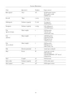
Glass
manufacturing
35%
Chemicals
&pigments
20%
Electronics
& photocopier
components 12%
Other
33%
Source:
Historical Statistics for Mineral and
Material Commodities in the United States
U.S. Geological Survey, 2005, selenium statistics, in T. D.
KellyandG.R.Matos,comps.,
,U.S.GeologicalSurvey
Data Series 140. Available online at />2005/140/.
U.S. End Uses of Selenium
tor devices, including radios, diodes, microproces
-
sors, computer chips, cellular phones, and power
grids, utilize semiconductor materials. Integrated cir-
cuits comprise numerous interconnected semicon-
ductors. Current “smart” technology products com-
bine integrated circuits with power semiconductor
technology.
Technical Definition
Semiconductors are special materials that conduct
differently under different conditions and are fre-
quently silicon-based. Semiconductors can act as a
nonconductor or a conductor, depending on the po-
larity of electrical charge applied to it, thus leading to
the term “semiconductor.” A number of elements are
classified as semiconductors, including silicon, zinc,
and germanium. Other materials include gallium ar-
senide and silicon carbide. Because silicon is readily
obtained, it is the most widely used semiconductor
material. These compounds have the ability to con-
duct electrical current and can be regulated in the
amount of their conductivity. Semiconductor devices
operate by utilizing electronic properties of semicon-
ductor materials.
Description, Distribution, and Forms
Semiconductor materialtakes advantage of the move-
ment of electrons between materials with varied con-
ductive properties.Semiconductors, special materials
that are frequently silicon-based, have varying electri-
cal conductivity properties depending on specific
conditions. Electrical resistance properties of semi-
conductor materials fall somewhere between those of
a conductor and those of an insulator. Most semicon-
ductor devices contain silicon chips with impurities
embedded to conduct electricity under some condi-
tions and not others. Silicon is the material used most
frequently to create semiconductors. Applying an ex-
ternal electrical field to a semiconductor material
changes its resistance. The ability of a semiconductor
material to conduct electricity can be changed dra-
matically by adding other elements or “impurities,” a
process known as “doping.” A pure semiconductor
without impurities is called an “intrinsic” semicon-
ductor. The amount of impurity, or dopant, added to
a semiconductor determines its level of conductivity.
Semiconductors are used to control electricity flow-
ing through a circuit, to amplify a signal, or to turn a
flow of current on or off. Semiconductor devices uti
-
lize the electronic properties of semiconductor mate
-
rials and have replaced vacuum tubes in most applica
-
tions. They utilize conductivity of electricity in the
solid state compared with the gaseous state of a vac-
uum. Semiconductor devices are manufactured both
as discrete devices and as integrated circuits that con-
sist of numerous devices, ranging from a few to mil-
lions, manufactured and interconnected on a single
semiconductor substrate. Typical semiconductor cir-
cuits include a combination of transistors, diodes, re-
sistors, and capacitors that function in switching, reg-
ulating, resisting, and storing electricity. Combining
smaller circuits such as these can be used to produce
integrated circuits, sensors,and microcontroller chips.
These devices are important in a broad spectrum of
consumer products and business equipment. Devices
made from semiconductor materials are the founda-
tion of modernelectronics,includingradios, comput-
ers, telephones, solar cells, andmanyotherdevices.In
fact, semiconductors serve as the essential compo-
nent in almost every modern electronic device.
Silicon, which is extracted from sand, is the most
common semiconductor material. In the 1990’s, there
was a tremendous growth in the semiconductor mate-
rials industry. The increase in production of com-
puters increased the need for semiconductors, with
major industry centers emerging in South Korea, Tai-
wan, Singapore, Malaysia, and Hong Kong.
History
Semiconductor materials were studied inlaboratories
as early as 1830. Over the years, many semiconductor
materials have been researched. The first materials
studied were a group of elements and compounds
that were generally poor conductors if heated.
Shining light on some of them would generate an
electrical current that could pass through them only
in one direction.
In the electronics field, semiconductors were used
for some time before the invention of the transistor.
By 1874, electricity was used not only to carry power
but also to carry information. The telegraph, the tele-
phone, and, later, the radio were the earliest devices
in an industry that would later be called electronics.
In the early part of the twentieth century, semicon-
ductors became common as detectors in radios, used
in a device called a “cat’s whisker.” The cat’s whisker
diode was created using the galena crystal, a semicon-
ductor material composed of lead sulfide, and was
considered the first semiconductor device. In the late
1950’s, a process called “planar technology” enabled
1080 • Semiconductors Global Resources
scientists todiffuse various layers onto the surface of a
silicon wafer to make a transistor with a layer of pro-
tective oxide in the junctions, making commercial
production of integrated circuits possible.
Obtaining Semiconductors
Most semiconductor chips and transistors are created
with silicon, because the material is easily obtained.
Semiconductors with predictable and reliable elec-
tronic properties are required for commercial pro-
duction of semiconductor devices. Because the pres-
ence ofeven smallamounts of impurities can result in
large effects on properties of the material, an ex-
tremely high level of chemical purity is necessary.
High crystalline perfection is also necessary because
faults in crystal structure interfere with semiconduct-
ing properties. Consequently, most semiconductors
are grown in laboratories as crystals. Commercial pro-
duction uses crystal ingots between 10 and 30 centi-
meters in diameter. These crystals are grown as cylin-
ders up to 2 meters in length and weighing several
hundred kilograms. They are sliced thin, into wafers
of standardized dimensions. The Czochralski process
is a method for growing single crystals of semiconduc-
tors and results in high-purity crystals.
Uses of Semiconductors
Semiconductor substances, commonly composed of
silicon, germanium, or compounds of gallium, are
the basisof integrated circuits controlling computers,
cell phones, and other electronic devices. Semicon-
ductors serve as essential components in almost every
electronic device in use. From outdated items such as
transistor radios to continuouslyevolvingonessuch as
the computer, semiconductors are responsible for
current technology. Modern semiconductor devices
include transistors, diodes, resistors, and capacitors.
They are found in televisions, automobiles, washing
machines, and computers. Automobiles use semicon-
ductors to control air-conditioning, injection pro-
cesses, ignition processes, sunroofs, mirrors, and steer-
ing. Anyitem that is computerized or uses radio waves
depends on semiconductors in order to function.
Power semiconductor devices combineintegratedcir-
cuits with power semiconductor technology, devices
often referred to as “smart” power devices. Semicon-
ductors serve essential roles in the control of motor
systems by optimizing a wide array of manufacturing
and industrial motor systems responsible for produc
-
tion of many diverse goods. Semiconductors are also
used in light-emitting diode lighting. All items that
use sensors or controllers rely on semiconductor ma-
terials.
Semiconductor-based power electronics are cru-
cial tools in the battle for energy efficiency. Semicon-
ductor technologies have enabled both performance
and energyefficiency improvements in telecommuni-
cation devices such as radios, televisions, emergency
response networks, and networking technology, pro-
cesses that require increasingly fast speeds and data-
management capabilities. Semiconductors have
helped increase efficiency of transportation in the
United States, with automobiles increasing their fuel
economy by more that 70 percent since 1980. Semi-
conductor technologies are used in diverse capacities
to enhance homelife, business, and personalcommu-
nications. Semiconductor technologies lead to indus-
trial productivity and enhanced energy efficiency and
use. Although there are many modern uses of semi-
conductors, their application in future devices ap-
pears unlimited.
C. J. Walsh
Further Reading
Anderson, Richard L., and Betty Lise Anderson. Fun-
damentals of Semiconductor Devices. New York:
McGraw-Hill, 2005.
Orton, John W. The Story of Semiconductors. New York:
Oxford University Press, 2009.
Singh, Jasprit. Semiconductor Devices: Basic Principles.
New York: Wiley, 2000.
Turley, Jim. The Essential Guide to Semiconductors.Up-
per Saddle River, N.J.: Pearson Education, 2003.
Yacobi, B. G. Semiconductor Materials: An Introduction to
Basic Principles. New York:KluwerAcademic,2003.
Web Sites
Nobel Prize.org
Semiconductors
/>physics/semiconductors/
U.S. Geological Survey
Mineral Information: Silicon Statistics and
Information
/>commodity/silicon/
See also: Fuel cells; Gallium; Germanium; Photovol
-
taic cells; Silicon.
Global Resources Semiconductors • 1081
Sewage disposal. See Solid waste
management; Waste management
and sewage disposal
Shale
Category: Mineral and other nonliving resources
Where Found
Shale is found throughout the world. It is the most
common of the three principal types of sedimentary
rock, that category ofrockformed by consolidationof
rock fragments or by chemical precipitation. In the
geologic record, for every approximate five units of
shale known, threeunits of sandstone andtwo units of
limestone (the remaining two common categories of
sedimentary rock) are also known.
Primary Uses
Shale is used as a filler in numerous construction ma-
terials. It is also used in everyday products such as cos-
metics and toothpaste, and as an energy source.
Technical Definition
Shale is a fine-grained consolidated rock principally
composed of silt-size (particles between 0.0039 and
0.0625 millimeter in diameter) and clay-size (lessthan
0.0039 millimeter in diameter) rock detritus. Shale is
generally characterized by a tendency to break along
well-defined bedding planes.
Description, Distribution, and Forms
The classification of shale is generally based on the
presence or absenceof well-defined bedding (lamina-
tion) planes. Fine-grained rock lacking thischaracter-
istic is termed mudstone, while a similar rock com-
posed entirely of clay-size material is known as
claystone. The ubiquityofshale is explained byits rep-
resenting approximately 75 percent of all sedimen-
tary rock produced throughout the entirety of geo-
logic time.
Because of their fine-grained nature, shales cannot
be conveniently examined mineralogically. Bulk
chemistry and X-ray studies show, however, that the
average shale iscomposed principally of thefollowing
oxides: silica (approximately 58 percent), aluminum
(approximately 15 percent), iron (approximately 7
percent), and calcium, potassium, and carbon (each
approximately 3 percent).
History
Shale richin organic materialdeposited bythe Missis-
sippi River over the past several tens of millions of
years caused the Gulf of Mexico to be one of the rich-
est hydrocarbon provinces in the world. Throughout
ten of the eastern United States and three western
states, the Chattanooga Shale and the Green River
Shale are identified as significant oil shale resources.
Obtaining Shale
Shale is aprime geologic source of crude oil andnatu-
ral gas (hydrocarbon). Hydrocarbon originates from
organic matter that accumulates in varieties of shale
generally deposited under marine conditions. The
preserved organic matter is converted to petroleum
and natural gasbyburial and related postdepositional
changes through the passage of geologic time. The
general lack of permeability of shale will later form a
barrier to the upper subsurface migration (and thus
to possible loss by surface evaporation) of generated
hydrocarbon.
Uses of Shale
Kaolinite-rich shale supplies the basic material for a
wide range of ceramic products, from pottery and
fine porcelain tosewer pipe. Shale richin barite isem-
ployed in thehydrocarbon industry topreventoil and
natural gas blowouts during the drilling of explor-
atory boreholes. Clay-rich shales are also employed in
the cosmetics, insulator, printing ink, medicine, and
toothpaste industries. The highly indurated form of
shale known as slate is used in the construction indus-
try as roofing and paving material. One major eco-
nomic importance of shale is associated with the
worldwide distribution of oil shale, a dark-colored
rock containing 5 to more than 25 percent solid or-
ganic material,from which oil can be extracted by dis-
tillation. Shale rich in organic material also acts di-
rectlyas a primary source of crudeoiland natural gas.
Albert B. Dickas
Web Sites
Natural Resources Canada
Stone
/>indu/cmy-amc/content/2006/56.pdf
1082 • Shale Global Resources
U.S. Geological Survey
Stone, Dimension
/>commodity/stone_dimension/myb1-2007-
stond.pdf
See also: Limestone; Oil and natural gas formation;
Oil andnatural gasreservoirs; Oilshale andtar sands;
Sandstone; Sedimentary processes, rocks, and min-
eral deposits.
Siemens, William
Category: People
Born: April 4, 1823; Lenthe, Prussia (now in
Germany)
Died: November 19, 1883; London, England
Siemens was an inventor whose work included the
steam engine and the regenerative furnace. He was
also a part of Siemens Brothers, a company formed
with four of his brothers, which is credited for ad-
vanced work on telegraph cables. Late in life, he pro-
posed the use of wind and water toproduce electricity.
Biographical Background
Charles William Siemens was born Karl Wilhelm Sie-
mens to Christian Ferdinand Siemens and Eleonore
Deichmann. Scientific education was provided at an
industrial school in Magdeburg, Germany, at the Uni-
versity of Göttingen, and at the works of Count Stol-
berg in Magdeburg.
Siemens spent mostof his life workinginsuccessful
collaborative relationships with four of his brothers.
His work with oldest brother Werner was often in the
area of electrical discovery, while collaboration with
Frederick led to the regenerative furnace. The sib-
lings eventually opened a company called Siemens
Brothers in 1858.
Siemens married Anne Gordon on July 23, 1859,
becoming a naturalized British citizen that same year.
The couple had no children. Siemens died in 1883 of
heart disease, leaving instructions in his will that the
papers pertaining to his scientific work were to be
published. Though not all of his experiments had
been successful, Siemens took copious notes thatpro
-
vide the basis of scientific research in a number of
areas.
Impact on Resource Use
Siemens’s inventions centered on preserving and us-
ing resources produced through natural or estab-
lished power sources. This work progressed after Sie-
mens went toEnglandin 1843 to impartknowledge of
his electrical discoveries. In 1847, he settled in Man-
chester and began work on the steam engine. This
work suggested the harnessing of energy from heat
combustion and recycling it into a working power
source. In 1850, the Society of Arts awarded him a
gold medal for his invention of the regenerative con-
denser. He also earned the Telford Premium and
medal of the Institution of Civil Engineers in 1853 for
this work.
In the same decade, he reaped financial rewards
from the success of his water meter; it sold so well, he
was able to live off the royalties. The water meter used
water energy to power a screw-turned meter. Siemens
received a patent for the fluid meter onApril 15,1852.
The patent also allowed for an application of the
water-powered screw to a meter that measured ship
speed.
Moving to London that year, he became an inde-
Global Resources Siemens, William • 1083
William Siemens invented the regenerative furnace. (Time & Life
Pictures/Getty Images)
pendent civil engineer. With Frederick, he continued
working on fine-tuning his steam engine. The two
men developed the regenerative furnace, which Fred-
erick patented in 1856. The regenerative furnace was
an expansion on the regenerative condenser.
In 1858, the brothers started a small factory, which
eventually became known as Siemens Brothers. Here,
the brothers’ work moved in a different direction.
Werner’s work on insulation of telegraph wiring was
so successful that the company was given responsibil-
ity for laying many telegraph lines both in England
and abroad. William’s major contribution during this
period was his design of a cable-laying ship.
Toward the end of his life, Siemens shifted his in-
terest back to electricity, and in 1877 he extended his
earlier work by proposing an expanded use of power
transmitted through water and wind sources. As a re-
sult, the family company became known for power
transmission. He spent his later years studying, lectur-
ing, and traveling.
Theresa L. Stowell
See also: Electrical power; Hydroenergy; Steam and
steam turbines; Steam engine; Wind energy.
Sierra Club
Category: Organizations, agencies, and programs
Date: Established 1892
The Sierra Club was founded in order to preserve U.S.
natural habitats for future generations. Fromits incep-
tion, the Sierra Club has made its goals the conserva-
tion of nature, the education of the public concerning
the preservation of nature, and the enjoyment of the
great outdoors.
Background
The Sierra Club was foundedin 1892 inSan Francisco
by 182 charter members led by John Muir. Muir and
the othermembers incorporated the Sierra Club with
the mission, as stated by Michael Cohen, “to explore,
enjoy, and render accessible the mountain regions of
the Pacific Coast, to publish authentic information
concerning them,” and “to enlist the support and co-
operation of the people and government in preserv
-
ing theforests and other natural features of the Sierra
Nevada.”
Impact on Resource Use
The Sierra Club has been influential in helping to
gain national parkstatus for Yosemite, Mount Rainier,
and numerous other important sites. Its members
have served on important governmental committees
and have spurred the enactment of many pieces of
legislation designed to conserve natural resources.
The club also leads expeditions large and small that
enable people to experience the wilderness.
The Sierra Club continues to work to ensure that
the legacy of clean air, water, soil, and wilderness will
remain for generations to come. It publishes a num-
ber of periodicals that help to educate the public con-
cerning the need to preserve American natural re-
sources.
Judy Arlis Chesen
Web Site
Sierra Club
/>See also: Conservation; Izaak Walton League of
America; Muir, John; National parks and nature re-
serves; National Wildlife Federation; Nature Conser-
vancy; Wilderness; Wilderness Society.
Silicates
Category: Mineral and other nonliving resources
The two most common elementsin the Earth’s crust are
silicon and oxygen. The prevalence of these two ele-
ments and their ability to combine as stable complex
ions accounts for the fact that silicate minerals consti-
tute a major portion of the minerals in Earth’s crust.
Their wide range of physical properties leads to many
commercial uses.
Definition
Silicon and oxygen combine to form stable complex
ions composed of one silicon ion surrounded by four
oxygen ions. Theresulting complex ion isa four-sided
figure known as a tetrahedron. Silicate tetrahedra
may exist independently separated by cations or link
together by sharing oxygens to form a wide range of
structural groupings. Tetrahedra groupings act as
skeletons in which charge neutrality is attained by
the addition of cations between and within silicate
1084 • Sierra Club Global Resources
tetrahedra. Silicate skeletons may exist as isolated
tetrahedran; as two tetrahedra sharing one oxygen
atom; as rings of three, four, or six tetrahedra; as
single and doublechains;as sheets; andascontinuous
three-dimensional frameworks. These skeletal arrange-
ments impart many diverse physical characteristics to
the various silicate minerals.
Overview
No generalizationdescribes allsilicates, although most
are translucent to transparent, have moderate spe-
cific gravity, and are chemically inert. Silicates range
from extremely soft to hard. Some display excellent
cleavage, but others are uniformly resistant to break-
ing in all directions.
Because silicate minerals exhibit such a wide varia-
tion in physical properties, they have variable com-
mercial uses. Talc, a magnesium silicate, is used as a
filler in paint, ceramics, rubber, insecticides, roofing,
and paper. Its most familiar form is as talcum powder.
Clay minerals (extremely small platy grains of hy-
drous aluminum silicates) are important industrial
minerals. They are used in a variety of fired products,
ranging from bricks to fine china and porcelain. Clay
is used as a filler in many products, including paper.
Montmorillonite, an expandable clay, is widely used
as a sealant. Zeolites, which are hydrous silicates with
open tunnels within a framework lattice, are widely
used as molecular sieves and for ion exchange resins;
they are valuable for oil-spill cleanup and wastewater
treatment and are used in water softeners.
In many applications, natural silicate minerals have
been replaced by the industrial manufacture of syn-
thetic and substitute materials. Muscovite mica, a
sheet structure, was used largely as an electrical insu-
lator in capacitors and electronic tubes. Asbestos, a
term describingflexible, fibroussilicatematerials, was
widely used for its heat resistance and its ability to
be woven as a fabric in fire-retardant cloth, in heat-
resistant sheets, in blown insulation, and in brake lin-
ings. Almost all asbestos use is outlawed in the United
States, as it is considereda carcinogen. Quartz (silicon
dioxide) is used as anabrasive,asopticalcomponents,
and as thin wafers to control the frequency of radio
and radar transmission. Quartz crystals are now grown
by commercial hydrothermal processes.
Many semiprecious stones are silicate minerals.
Microcrystalline varieties of quartz that are used in
jewelry include fibrous-appearing tiger’s eye, red jas
-
per, multicolored agate, and the red-spotted blood
-
stone. Crystalline varieties ofquartzthat serve as semi
-
precious stones include yellow citrine and violet
amethyst. Topaz, jade, garnet, opal, and peridot are
silicates, as is emerald, which is gem-quality beryl.
René A. De Hon
See also: Asbestos; Clays; Feldspars; Mica; Minerals,
structure and physical properties of; Orthosilicate
minerals; Quartz; Silicon; Talc.
Silicon
Category: Mineral and other nonliving resources
Where Found
Silicon makes up 25.7 percent of theEarth’s crustand
is the second most abundant element after oxygen. It
is not found in itselementalform, but rather occurs in
compounds such as oxides and various silicate miner-
als. Silicon is a trace element participating in the
metabolism of higher animals, and siliceous struc-
tures are found in manybiologicalsystems in the form
of cell walls, scales, and other skeletal features.
Primary Uses
Silicon metal and alloys, including ferrosilicon, are
used mainlyby producers of aluminum, aluminum al-
loys, and chemicals. Very pure silicon is an essential
component of semiconductorsandhas given its name
to the “silicon age,” a termthat came into prominence
during the 1990’s.
Technical Definition
Silicon (abbreviated Si) is the fourteenth element of
the periodic table, with an atomic number of 28. With
carbon, germanium, and tin, it belongs to Group IVA
of the periodic table and resembles germanium (Ge)
most strongly in its physical, chemical, and electronic
properties. Pure silicon is a hard, gray solid with a me-
tallic luster and a cubic crystalline structure similar to
that of carbon in diamond form. It has eight isotopes,
the most abundant of which are Si
28
(92.23 percent),
Si
29
(4.67 percent), and Si
30
(3.10 percent). Its density
is 2.329 grams per cubic centimeter, and it has a melt-
ing point of 1,410° Celsius and a boiling point of
2,355° Celsius. While the single-crystal form of silicon
has been most extensively studied from both basic
and practical viewpoints, the polycrystalline and
Global Resources Silicon • 1085
amorphous forms of silicon have also become ex-
tremely important: Polycrystalline silicon has been
applied in the construction of solar panels and cen-
tral processing units of computers. Amorphous sili
-
con has been used in thin-film transistors and solar
cells.
Description, Distribution, and Forms
Silicon is widely available in oxides and silicates. The
oxide forms include sand, quartz, rock crystal, ame-
thyst, agate, flint,andopal. Granite, feldspar, clay, and
mica are some of the common forms of silicates. A ba
-
sic requirement of silicon in all its preeminent elec
-
1086 • Silicon Global Resources
Data from the U.S. Geological Survey, . U.S. Government Printing Office, 2009.Source: Mineral Commodity Summaries, 2009
39,000
340,000
640,000
140,000
78,000
85,000
166,000
60,000
Metric Tons of Silicon Content
3,500,0003,000,0002,500,0002,000,0001,500,0001,000,000500,000
Venezuela
Spain
South Africa
Russia
Norway
Macedonia
Ukraine
United States
Other countries
66,000
3,300,000
160,000
74,000
39,000
68,000
Iceland
France
China
Canada
Brazil
India
Kazakhstan
180,000
270,000
Silicon: World Production, 2008
tronic applications is extreme purity—to levels much
better than parts per billion (ppb).
The single-crystal form of silicon, while essential
for computer chips, has cost and size limitations for a
host of other potentially high-volume applications.
Hence silicon is also produced in polycrystalline and
amorphous forms by techniques such as casting and
thin-film deposition. Polycrystalline forms (poly-Si)
contain crystalline grains separated by grain bound-
aries, while amorphous silicon lacks the long-range
crystalline order completely. However, both have use-
ful semiconducting properties and have been widely
developed for a range of uses.
The interesting and extremely useful electronic
and optoelectronic properties of silicon stem from its
tetrahedral bonding and diamond cubic structure.
Replacing a host silicon atom with a Group V element
(such as phosphorus) or Group III element (such as
boron) adds a free electron or “hole” (an electron va-
cancy that behaves like a positively charged free parti-
cle. Thus the electrical conductivity of silicon can be
changed over several powers of ten simply by control-
ling the trace quantities of phosphorus or boron. The
bandgap separating the electron and hole states has a
value of 1.12 electron volts for silicon, making it a
nearly ideal choice for devices as varied as transistors,
diodes, solar cells, and various types of sensors.
Optically, silicon is transparent to infrared wave-
lengths above 1.1 micrometers while it absorbs thevis-
ible spectrum. Silicon is brittle, but its highly direc-
tional bonds enable easy “scribing” of the silicon
wafer into individual computer chips under properly
chosen crystal orientations. The intricate chemical
properties ofsilicon enable deployment of avariety of
fabrication techniques, with individual feature sizes
falling into the submicron regime. The modest ther-
mal conductivity of silicon places some restraints on
thermal dissipation in computer chips.
History
Although many chemists recognized silicon as an ele-
ment by the early nineteeth century, its tight bonding
with oxygen made it difficult to isolateas a separate el-
ement. Jöns Jacob Berzelius achieved the isolation of
silicon in 1823 using a method similar to one devel-
oped by Sir Humphy Davy, who earlier had tried but
failed to isolate silicon. The newly isolated element
was named for the Latin wordforflint,silex,andsubse
-
quently was investigated by German chemist Friedrich
Wöhler and others.
Obtaining Silicon
Semiconductor-grade silicon requires conversion of
raw silicon obtained from reducing silica (SiO
2
) into
gaseous compounds such as chlorosilanes. Multiple
fractional distillation of the latter leads to high-purity
silicon rods. These rods are subsequently melted and
grown into dislocation-free single crystals by either
the Czochralski (CZ) crystal pulling process or the
float zone (FZ) process. Necessary dopants such as
boron (for p-type silicon) andphosphorus(for n-type
silicon) are added to the melt. CZ silicon ingots are
probably the largest single crystals ever produced—
more than 3 meters long, with diameters as large as
300 millimeters. Wafers, about a millimeter thick,
sliced from the ingots serveasthe starting materialfor
the batch fabrication of microelectronic chips, each
containing up to a few million transistors.
Silicon by itself is inert, but a number of source
gases and reagents used in manufacturing it are highly
toxic, so extreme care must be exercised in waste dis-
posal and protection of assembly workers. Silicon has
been implicated in silicotic lung diseases and certain
cancers.
Uses of Silicon
The principal applications of high-grade silicon are
in microelectronics. The atomic structure of crystal-
line silicon makes it the most important semiconduc-
tor. Silicon in its highly purified form, when “doped”
with elements such as boron and phosphorus, be-
comes the basic element of computer chips, transis-
tors, diodes, and various other electronic switching
and control devices. The enormous success of the sili-
con transistor, the basic electronic amplifying device,
was made possible by an extremely pristine interface
with silicon dioxide (an insulator readily grown on sil-
icon by heating in oxygen) and by the continual scal-
ing down oftransistor feature size, whichtranslates di-
rectly to faster computer speed and higher memory
capacity.
The fieldof giant microelectronics, exemplified by
portable computer displays and flat-screen television,
uses silicon in its polycrystalline or amorphous forms.
Another area of great impact for silicon is in terres-
trial solar cells, for which extremely large volumes at
low cost are necessary. Here computer-grade single
crystals are not cost-effective; large-grain polycrys-
talline silicon holds the key for this crucial renewable
energy application.
A late-twentieth century silicon technology ex
-
Global Resources Silicon • 1087