Electric Circuits, 9th Edition P55 pot
Bạn đang xem bản rút gọn của tài liệu. Xem và tải ngay bản đầy đủ của tài liệu tại đây (784.51 KB, 10 trang )
516 The Laplace Transform in Circuit Analysis
Figure P13.61
h(t)'
10
40 40 /
(a)
*(0"
4
h(ty
40
0 10 t
(b)
0 1
(c)
13.62 A rectangular voltage pulse
i>,-
= [«(/) - u(t - 1)] V
is applied to the circuit in Fig. P13.62. Use the con-
volution integral to find v
n
.
>•',
in:
13.63 Interchange the inductor and resistor in
Problem 13.62 and again use the convolution inte-
gral to find v
Q
.
13.65 a) Repeat Problem 13.64, given that the resistor in
the circuit in Fig. PI3.50(a) is decreased to 10 kll.
b) Does decreasing the resistor increase or decrease
the memory of the circuit?
c) Which circuit comes closer to transmitting a
replica of the input voltage?
13.66 a) Assume the voltage impulse response of a
circuit is
//.(/)
0, t < 0;
lOtT
4
', t > 0.
Use the convolution integral to find the output
voltage if the input signal is 10*<(0 V.
b) Repeat (a) if the voltage impulse response is
0, t < 0;
= \ 10(1 - 20, 0 < t < 0.5 s;
0, t > 0.5 s.
c) Plot the output voltage versus time for (a) and
(b) for 0 < t < 1 s.
13.67 The voltage impulse response of
a
circuit is shown in
Fig. P13.67(a). The input signal to the circuit is the
rectangular voltage pulse shown in Fig. P13.67(b).
a) Derive the equations for the output voltage.
Note the range of time for which each equation
is applicable.
b) Sketch v
0
for -1 < t < 34 s.
13.64 a) Use the convolution integral to find the output
voltage of the circuit in Fig. P13.50(a) if the
input voltage is the rectangular pulse shown in
Fig. P13.64.
b) Sketch v
0
(t) versus t for the time interval
0 < t < 10 ms.
Figure P13.64
»i(V)
lo
r(ms)
Problems 517
13.68 Assume the voltage impulse response of a circuit
can be modeled by the triangular waveform shown
in Fig. P13.68.The voltage input signal to this circuit
is the step function 10«(^) V.
a) Use the convolution integral to derive the
expressions for the output voltage.
b) Sketch the output voltage over the interval
0 to 15 s.
c) Repeat parts (a) and (b) if the area under the
voltage impulse response stays the same but the
width of the impulse response narrows to 4 s.
d) Which output waveform is closer to replicating
the input waveform: (b) or (c)? Explain.
Figure P13.68
A(0 (V)
10
«(»)
13.69 a) Find the impulse response of the circuit shown
in Fig. P13.69(a) if v
g
is the input signal and v
0
is
the output signal.
b) Given that v
q
has the waveform shown in
Fig. P13.69(b), use the convolution integral to
find v
a
.
c) Does v
a
have the same waveform as v
g
l Why or
why not?
Figure P13.69
4H
v
g
(V)
75
0
-75
0.5
1.0
t(s)
(a)
(b)
13.70 a) Find the impulse response of the circuit seen in
Fig. PI3.70 if v
g
is the input signal and v
n
is the
output signal.
b) Assume that the voltage source has the wave-
form shown in Fig. P13.69(b). Use the convolu-
tion integral to find v
(r
c) Sketch % for 0 < / < 2 s.
d) Does v
a
have the same waveform as v„l Why or
why not?
Figure P13.70
13.71 The sinusoidal voltage pulse shown in Fig. P13.71(a)
is applied to the circuit shown in Fig. P13.71(b). Use
the convolution integral to find the value of v
()
at
t = 75 ms.
Figure P13.71
5H
v, 160 n-
77/20 ir/io r(s)
(b)
13.72 Use the convolution integral to find v
(
, in the circuit
seen in Fig. P13.72 if v
t
= 75u{t) V.
Figure P13.72
40 0
o Vs/V—
4H
J-TYYV
4
16
H
13.73 The current source in the circuit shown in
Fig. P13.73(a) is generating the waveform shown in
Fig. PI 3.73(b). Use the convolution integral to find
v„ at t = 5 ms.
518 The Laplace Transform in Circuit Analysis
Figure P13.73
i
g
(mA)
10
H—I—I—
1 2 3 4
-20 4
(b)
5 6
t (ms)
0.4 /itF
(a)
Figure P13.75
i„
{fiA)
50
0
-50
(b)
100
200
/(ms)
(a)
13.74 The input voltage in the circuit seen in Fig. PI 3.74 is
V; = 5[u(t) - u(t - 0.5)] V.
a) Use the convolution integral to find v
a
.
b) Sketch v
a
for 0 < t < 1 s.
Figure P13.74
20
• /vv—
100
mH
100
mF
13.76 a) Show that if y(t) = h(() * x(t), then Y{s)
H(s)X(s).
b) Use the result given in (a) to find /(f) if
F(s) =
s(s + a)"
Section 13.7
13.77 The transfer function for a linear time-invariant
circuit is
13.75 a) Use the convolution integral to find v
0
in the cir-
cuit in Fig. P13.75(a) if i
s
is the pulse shown in
Fig. PI3.75(b).
b) Use the convolution integral to find i
0
.
c) Show that your solutions for v
v
and
i
(
,
are consis-
tent by calculating v
a
and i
n
at 100" ms,
100
+
ms, 200" ms, and 200
+
ms.
H(s)
V
0
4(s + 3)
V
g
s
2
+ 8s + 41
If v
K
= 40 cos 3/ V, what is the steady-state expres-
sion for v
a
'l
13.78 When an input voltage of 30u(t) V is applied to a
circuit, the response is known to be
-80(H)/
111)0,
v
a
= (50*-*™" - 20e-™*")u{t) V.
What will the steady-state response be if
v
g
= 120 cos 6000/ V?
Problems 519
13.79 The op amp in the circuit seen in Fig. P13.79 is ideal.
PSPKE
a) Find the transfer function
VJV„.
MULTISIM ' "' S
b) Find v
a
if v
g
= 0.6//(0 V.
c) Find the steady-state expression for v„ if
v
g
= 2 cos 10,000/: V.
Figure P13.79
13.82 The inductor L
x
in the circuit shown in Fig. P13.82
is carrying an initial current of p A at the instant
the switch opens. Find (a) v(t); (b)
/
-
i(/);
(c) i
2
(t)',
and (d) A(r), where A(f) is the total flux linkage in
the circuit.
Figure P13.82
y„*15kll
13.80 The operational amplifier in the circuit seen in
PSPICE pig. P13.80 is ideal and is operating within its lin-
MULTISIM
ear region.
a) Calculate the transfer function
V„/V
R
.
b) If v
g
= 2cos400f V, what is the steady-state
expression for
v
(>
'~!
'ifPTU
R
«2i:
13.83 a) Let R -» oo in the circuit shown in Fig. P13.82,
and use the solutions derived in Problem 13.82
to find v(t),
ii(t),
and i
2
{t).
b) Let R = oo in the circuit shown in Fig. P13.82
and use the Laplace transform method to find
-u(f),
ii(t),
and i
2
{t).
13.84 There is no energy stored in the circuit in Fig. P13.84
at the time the impulsive voltage is applied.
a) Find v
(>
(t) for t > 0.
b) Does your solution make sense in terms of
known circuit behavior? Explain.
Figure P13.80
y
r>
520kn
Section 13.8
13.81 Show that after
V^C
C
coulombs are transferred from
C] to C
2
in the circuit shown in Fig. 13.47, the volt-
age across each capacitor is
C\V
{)
f(C\
+ C
2
). (Hint:
Use the conservation-of-charge principle.)
Figure P13.84
200
H
4 mH
55(/) mV
16
mH
13.85 The parallel combination of R
2
and C
2
in the circuit
shown in Fig. P13.85 represents the input circuit to
a cathode-ray oscilloscope (CRO). The parallel
combination of i?j and C\ is a circuit model of a
compensating lead that is used to connect the CRO
to the source. There is no energy stored in C\ or C
2
at the time when the
10
V source is connected to the
CRO via the compensating lead. The circuit values
are Q = 4 pF, C
2
= 16 pF, R
l
= 1.25 Mft, and
R
2
= 5 MH.
a) Find v
a
.
b) Find i
0
.
c) Repeat (a) and (b) given Cj is changed to 64 pF
520 The
Laplace Transform
in
Circuit
Analysis
Figure
P13.85
13.89 Tliere is no energy stored in the circuit in Fig. P13.89
at the time the impulsive current is applied.
a) Find v
()
for t > ()
+
.
b) Does your solution make sense in terms of
known circuit behavior? Explain.
Figure
P13.89
250 nF
13.86 Show that if R\C\ = RiC
2
in the circuit shown in
Fig. P13.85, v
(>
will be a scaled replica of the
source voltage.
13.87 The switch in the circuit in Fig. PI3.87 has been
closed for a long time. The switch opens at t — 0.
Compute (a) «,((T); (b)
/,(0
+
);
(c) /
2
(<T); (d) /
2
((T);
(e) i!(r); (f) /
2
(0; and (g) v{t).
Figure
P13.87
t = 0
1
= uv
5A
©
+
:8 mH
::•! 0 jr
1
v(t) k\\
4kO |16kH
13.90 The voltage source in the circuit in Example 13.1 is
changed to a unit impulse; that is, v
g
= 8(t).
a) How much energy does the impulsive voltage
source store in the capacitor?
b) How much energy does it store in the inductor?
c) Use the transfer function to find v
a
(t).
d) Show that the response found in (c) is identical
to the response generated by first charging the
capacitor to 1000 V and then releasing the
charge to the circuit, as shown in Fig. P13.90.
Figure P13.90
looon
k
-1-*
^ r> < . i
1000 V
13.88 The switch in the circuit in Fig. P13.88 has been in
position a for a long time. At t = 0, the switch
moves to position b. Compute (a) ^(O
-
); (b) y?(0
_
);
(c) v
3
(0-); (d) i(t); (e)
^(0
+
);
(f) v
2
(0
+
){ and
(g)^3(0
+
).
Figure P13.88
—'VW-
20kfl
100 v
(-)
A
0.5 ^F;
2.0/XF;
r = 0
+
+
13.91 There is no energy stored in the circuit in Fig. P13.91
at the time the impulse voltage is applied.
a) Find i
{
for t > 0
+
.
b) Find i
2
for t > 0
+
.
c) Find v
a
for t > 0
+
.
d) Do your solutions for i
u
/
2
, and v
(}
make sense in
terms of known circuit behavior? Explain.
i(0
1.6
IJLF:
+
:¾
Figure P13.91
0.5 H
1>"~
205(/) V
©
IH:
1H jF.
Problems 521
Sections 13.1-13.8
13.92 Assume the line-to-neutral voltage Y
0
in the 60 Hz
mom
circuit
of Fig- 13.59 is 120 /CT V (rms). Load
R
CI
is
absorbing 1200 W; load R
b
is absorbing 1800
W;
and
load X
a
is absorbing 350 magnetizing VAR. The
inductive reactance of the line (X{) is 1 fl. Assume
V<,
does not change after the switch opens.
a) Calculate the initial value of i
2
(t) and
i[
0
(t).
b) Find V
0
, v
()
(t), and v
()
(Q
+
) using the s-domain
circuit of Fig. 13.60.
c) Test the steady-state component of v
a
using pha-
sor domain analysis.
d) Using a computer program of your choice, plot
v
0
vs.
t for 0 £ t < 20 ms.
13.93 Assume the switch in the circuit in Fig. 13.59
'ERSPECTIVE
°P
ens
al tne
instant the sinusoidal steady-state
voltage v
a
is zero and going positive, i.e.,
v
0
= 120V2~sinl207rtV.
a) Find v
0
{t) for t > 0.
b) Using a computer program of your choice, plot
v
0
(t)
vs.
t for 0 < t < 20 ms.
c) Compare the disturbance in the voltage in
part (a) with that obtained in part (c) of
Problem 13.92.
13.94 The purpose of this problem is to show that the
•ERSPEcnvE li
ne
-t°-
neutra
l voltage in the circuit in Fig. 13.59
can go directly into steady state if the load R
h
is
disconnected from the circuit at precisely the
right time. Let v
0
= V
m
cos(
12077/
- 0°) V, where
V
m
= 120
V2.
Assume v
g
does not change after R
b
is disconnected.
a) Find the value of 6 (in degrees) so that v
0
goes
directly into steady-state operation when the
load R
f)
is disconnected.
b) For the value of
6
found in part (a), find %(t) for
t > 0.
c) Using a computer program of your choice, plot
on a single graph, for -10 ms ^ t ^ 10 ms,
v
a
(t) before and after load R
b
is disconnected.
I
CHAPTER CONTENTS
14.1 Some Preliminaries p. 524
14.2 Low-Pass Filters p. 526
14.3 High-Pass Filters p. 532
14.4 Bandpass Filters p. 536
14.5 Bandreject Filters p. 545
Know the RL and RC circuit configurations that
act as low-pass filters and be able to design
RL and RC circuit component values to meet a
specified cutoff frequency.
Know the
RL
and
RC
circuit configurations that
act as high-pass filters and be able to design
RL
and
RC
circuit component values to meet a
specified cutoff frequency.
Know the
RLC
circuit configurations that act as
bandpass filters, understand the definition of
and relationship among the center frequency,
cutoff frequencies, bandwidth, and quality
factor of a bandpass filter, and be able to
design
RLC
circuit component values to meet
design specifications.
Know the
RLC
circuit configurations that act as
bandreject filters, understand the definition of
and relationship among the center frequency,
cutoff frequencies, bandwidth, and quality
factor of a bandreject filter, and be able to
design
RLC
circuit component values to meet
design specifications.
522
Introduction to Frequency
Selective Circuits
Up to this point in our analysis of circuits with sinusoidal
sources, the source frequency was held constant. In this chapter,
we analyze the effect of varying source frequency on circuit volt-
ages and currents. The result of this analysis is the frequency
response of
a
circuit.
We've seen in previous chapters that a circuit's response
depends on the types of elements in the circuit, the way the ele-
ments are connected, and the impedance of the elements.
Although varying the frequency of a sinusoidal source does not
change the element types or their connections, it does alter the
impedance of capacitors and inductors, because the impedance
of these elements is a function of frequency. As we will see, the
careful choice of circuit elements, their values, and their con-
nections to other elements enables us to construct circuits that
pass to the output only those input signals that reside in a
desired range of frequencies. Such circuits are called
frequency-selective circuits. Many devices that communicate
via electric signals, such as telephones, radios, televisions, and
satellites, employ frequency-selective circuits.
Frequency-selective circuits are also called filters because of
their ability to filter out certain input signals on the basis of fre-
quency. Figure 14.1 on page 524 represents this ability in a sim-
plistic
way.
To
be more accurate, we should note that no practical
frequency-selective circuit can perfectly or completely filter out
selected frequencies. Rather, filters attenuate—that
is,
weaken or
lessen the effect of—any input signals with frequencies outside
frequencies outside a particular frequency band. Your home
stereo system may have a graphic equalizer, which is an excellent
example of a collection of filter circuits. Each band in the graphic
equalizer is a filter that amplifies sounds (audible frequencies) in
the frequency range of the band and attenuates frequencies out-
side of that band. Thus the graphic equalizer enables you to
change the sound volume in each frequency band.
Practical Perspective
Pushbutton Telephone Circuits
In this chapter, we examine circuits in which the source
fre-
quency varies. The behavior of these circuits varies as the
source frequency varies, because the impedance of the reac-
tive components is a function of the source frequency. These
frequency-dependent circuits are called filters and are used
in many common electrical devices. In radios, filters are used
to select one radio station's signal while rejecting the signals
from others transmitting at different frequencies. In stereo
systems, filters are used to adjust the relative strengths of the
low- and high-frequency components of the audio signal.
Filters are also used throughout telephone systems.
A pushbutton telephone produces tones that you hear
when you press a button. You may have wondered about these
tones.
How are they used to tell the telephone system which
button was pushed? Why are tones used at all? Why do the
tones sound musical? How does the phone system tell the
dif-
ference between button tones and the normal sounds of peo-
ple talking or singing?
The telephone system was designed to handle audio
signals—those with frequencies between 300 Hz and 3 kHz.
Thus,
all signals from the system to the user have to be
audible—including the dial tone and the busy signal. Similarly,
all signals from the user to the system have to be audible,
including the signal that the user has pressed a button. It is
important to distinguish button signals from the normal audio
signal,
so a dual-tone-multiple-frequency (DTMF) design is
employed.
When a number button is pressed, a unique pair of
sinusoidal tones with very precise frequencies is sent by the
phone to the telephone system. The
DTMF
frequency and timing
specifications make it unlikely that a human voice could pro-
duce the exact tone pairs, even if the person were trying. In
the central telephone facility, electric circuits monitor the
audio signal, listening for the tone pairs that signal a number.
In the Practical Perspective example at the end of the chapter,
we will examine the design of the DTMF filters used to deter-
mine which button has been pushed.
523
524 Introduction to Frequency Selective Circuits
Input
signal
Filter
Output
signal
Figure 14.1 • The action of
a
filter
on
an input signal
results in an output signal.
We begin this chapter by analyzing circuits from each of the four
major categories of filters: low pass, high pass, band pass, and band reject.
The transfer function of a circuit is the starting point for the frequency
response analysis. Pay close attention to the similarities among the trans-
fer functions of circuits that perform the same filtering function. We will
employ these similarities when designing filter circuits in Chapter 15.
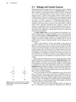
14.1 Some Preliminaries
Vi(s)
Figure 14.2 A
A
circuit with voltage input and output.
Recall from Section 13.7 that the transfer function of a circuit provides an
easy way to compute the steady-state response to a sinusoidal input. There,
we considered only fixed-frequency sources. To study the frequency response
of a circuit, we replace a fixed-frequency sinusoidal source with a varying-
frequency sinusoidal source. The transfer function is still an immensely useful
tool because the magnitude and phase of the output signal depend only on
the magnitude and phase of the transfer function H{ja)).
Note that the approach just outlined assumes that we can vary the fre-
quency of a sinusoidal source without changing its magnitude or phase
angle. Therefore, the amplitude and phase of the output will vary only if
those of the transfer function vary as the frequency of the sinusoidal
source is changed.
To further simplify this first look at frequency-selective circuits, we will
also restrict our attention to cases where both the input and output signals
are sinusoidal voltages, as illustrated in Fig.
14.2.
Thus, the transfer function
of interest to us will be the ratio of the Laplace transform of the output volt-
age to the Laplace transform of the input voltage, or H(s) — V
0
(s)/Vi(s).
We should keep in mind, however, that for a particular application, a current
may be either the input signal or output signal of interest.
The signals passed from the input to the output fall within a band of
frequencies called the passband. Input voltages outside this band have
their magnitudes attenuated by the circuit and are thus effectively pre-
vented from reaching the output terminals of the circuit. Frequencies not
in a circuit's passband are in its stopband. Frequency-selective circuits are
categorized by the location of the passband.
One way of identifying the type of frequency-selective circuit is to
examine a frequency response plot. A frequency response plot shows how
a circuit's transfer function (both amplitude and phase) changes as the
source frequency
changes.
A frequency response plot has two parts. One is
a graph of \H(jai)\ versus frequency w. This part of the plot is called the
magnitude plot. The other part is a graph of d(Jw) versus frequency
w.
This
part is called the phase angle plot.
The ideal frequency response plots for the four major categories of fil-
ters are shown in Fig. 14.3. Parts (a) and (b) illustrate the ideal plots for a
low-pass and a high-pass filter, respectively. Both filters have one pass-
band and one stopband, which are defined by the cutoff frequency that
separates them. The names low pass and high pass are derived from the
magnitude plots: a low-pass filter passes signals at frequencies lower than
the cutoff frequency from the input to the output, and a high-pass filter
passes signals at frequencies higher than the cutoff frequency. Thus the
terms low and high as used here do not refer to any absolute values of fre-
quency, but rather to relative values with respect to the cutoff frequency.
Note from the graphs for both these filters (as well as those for the
bandpass and bandreject filters) that the phase angle plot for an ideal filter
varies linearly in the passband. It is of no interest outside the passband
because there the magnitude is zero. Linear phase variation is necessary to
avoid phase distortion.
\H(ja>)\
I
em
0°
9{ju
c
) -
Passband
1//(/0,)1
1
Stopband
d(jw
c
)
0° -
Stopband
Passband
(a)
(b)
d(ja>)
0°
0(/w
c2
)
h)\
Stopband
Pass-
band
Stopband
0)
cl
(O
c2
0)
\
- \
m
i
0°
0(M:l)
M
Passband
Stop
band
Passband
<u
c
] a>
C
2 (o
(c)
(d)
Figure 14.3 • Ideal frequency response plots of the four types of filter circuits,
(a)
An
ideal low-pass filter, (b)
An
ideal high-pass filter, (c)
An
ideal bandpass filter,
(d)
An
ideal bandreject filter.
The two remaining categories of filters each have two cutoff frequen-
cies.
Figure 14.3(c) illustrates the ideal frequency response plot of a
bandpass filter, which passes a source voltage to the output only when the
source frequency is within the band defined by the two cutoff frequencies.
Figure 14.3(d) shows the ideal plot of a bandreject filter, which passes a
source voltage to the output only when the source frequency is outside the
band defined by the two cutoff frequencies. The bandreject filter thus
rejects, or stops, the source voltage from reaching the output when its fre-
quency is within the band defined by the cutoff frequencies.
In specifying a realizable filter using any of the circuits from this chap-
ter, it is important to note that the magnitude and phase angle characteris-
tics are not independent. In other words, the characteristics of a circuit
that result in a particular magnitude plot will also dictate the form of the
phase angle plot and vice versa. For example, once we select a desired
form for the magnitude response of a circuit, the phase angle response is
also determined. Alternatively, if we select a desired form for the phase
angle response, the magnitude response is also determined. Although
there are some frequency-selective circuits for which the magnitude and
phase angle behavior can be independently specified, these circuits are
not presented here.
The next sections present examples of circuits from each of the four
filter categories. They are a few of the many circuits that act as filters. You
should focus your attention on trying to identify what properties of a cir-
cuit determine its behavior as a filter. Look closely at the form of the
transfer function for circuits that perform the same filtering functions.
Identifying the form of a filter's transfer function will ultimately help you
in designing filtering circuits for particular applications.
All of the filters we will consider in this chapter are passive filters, so
called because their filtering capabilities depend only on the passive