Three-Dimensional Integration and Modeling Part 4 pot
Bạn đang xem bản rút gọn của tài liệu. Xem và tải ngay bản đầy đủ của tài liệu tại đây (1.72 MB, 8 trang )
THREE-DIMENSIONAL PACKAGING IN MULTILAYER ORGANIC SUBSTRATES 21
FIGURE 3.10: Gain measurement of the Hittite HMC342 13–25 GHz LNA. The first measurement
was of the packaged/bonded MMIC. The second measurement was done immediately after the packaged
MMIC was submerged in water on edge for 48 h. The match of the measurements demonstrates as
successful seal by the LCP package. The minimal water absorption into the package shows no significant
effect on the MMIC performance.
The gain measurement in the before/after states is identical, indicating that the multilayer
LCP MMIC package method can be used successfully for packaging active devices.
3.4 THREE-DIMENSIONAL PAPER-BASED MODULES FOR
RFID/SENSING APPLICATIONS
As the demand for low-cost, flexible and efficient electronics increases, the materials and integra-
tion technologies become more critical and face many challenges, especially with the ever growing
interest for “cognitive intelligence” and wireless applications, such as radio frequency identifica-
tion (RFID) and wireless local area networks (WLAN). Paper has been considered as one of the
best organic-substrate candidates for ultrahigh frequency (UHF) and microwave applic ations such
as RFID/sensing. It is not only environmentally friendly, but can also undergo large reel-to-reel
processing. In terms of mass production and increased demand, this makes paper the lowest cost
material made. Paper also has low surface profile with appropriate coating. This is very crucial since
fast printing processes, such as direct write methodologies, can be utilized instead of metal etching
techniques. A fast process, like inkjet printing, can be used efficiently to print electronics on/in paper
substrates.
22 THREE-DIMENSIONAL INTEGRATION
FIGURE 3.11: Inductively coupled feeding RFID tag module configuration.
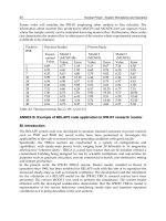
First of all, the RF characteristics of the paper-based substrate have been recently studied by
using the cavity resonator method and the transmission line method to characterize the dielectric
constant (ε
r
) and loss tangent (tan ı) of the substrate [60]. The results show ε
r
= 1.6 at Ka band and
tan ı<0.082 up to 2.4 GHz. Then, aUHF RFID tag module was developed with the inkjet-printing
technology that could function as a technology for much simpler and faster fabrication on/in paper.
Most available commercial RFID tags are passive, and the antenna translates electromagnetic waves
from the reader into power supplied to the IC. Thus, a conjugate impedance matching between
antenna and the tag IC is highly essential to power up the IC and maximize the effective range, and
so an inductively coupled feeding structure is an effective way for impedance matching.
FIGURE 3.12: Measured and simulated input resistance and reactance of the inkjet-printed RFID tag.
25
CHAPTER 4
Microstrip-Type Integrated Filters
4.1 PATCH RESONATOR FILTERS AND DUPLEXERS
4.1.1 Single Patch Resonator
Integrating filter-on-package in low-temperature cofired ceramic (LTCC) multilayer technology is a
very attractive option for radio frequency (RF) front-ends up to the millimeter-wave frequency range
in termsofbothminiaturization by vertical deployment offilterelementsandreductionof thenumber
of components and assembly cost by eliminating the demand for discrete filters. In millimeter-
wave frequencies, the bandpass filters are commonly realized using slotted patch resonators because
of their miniaturized size and their excellent compromise among size, power handling, and
easy-to-design layout [17]. In this section, the design of a single-pole slotted patch filter is presented
for two operating frequency bands (38–40 GHz and 58–60 GHz). This design can be easily gener-
alized to multiband applications, especially for portable wireless modules that the size and weight
is of paramount importance. Its major advantages are its capability of high-Q structures in vertical
stackups and the easy addition of multiple stages for high-selectivity applications.
Figure 4.1(a) and (b) shows a top-view comparison between a basic half-wavelength
(/2) square patch resonator (L ×L =0.996 mm ×0.996 mm) [61] and the new configuration
(L ×L =0.616 mm ×0.616 mm), respectively, that is capable of providing good tradeoffs between
miniaturization and power handling. Side views and the photographs of the 60 GHz resonators are
shown in Figs. 4.2 and 4.3, respectively. In the conventional design of a /2 square patch, the planar
single-mode patch and microstrip feedlines are located on metal 3 (M3 in Fig. 4.2) and they use
the end-gap capacitive coupling between the feedlines and the resonator itself to achieve 3% 3-dB
bandwidth and <3 dB insertion loss around the center frequency of 60GHz. However, the required
coupling capacitances to obtain design specifications could not be achieved because of the LTCC
design rule limitations.
To maximize the coupling strength while minimizing the effects of the fabrication, the pro-
posed novel structure takes advantage of the vertical deployment of filter elements by placing the
feedlines and the resonator into different vertical metal layers, as shown in Fig. 4.2. This transi-
tion also introduces a 7.6% frequency downshift resulting from the additional capacitive coupling
effect compared to the basic /2 square patch resonator [Fig. 4.1(a)] directly attached by feedlines.
Transverse cuts have been added on each side of the patch to achieve significant miniaturization of
the patch by contributing an additional inductance. Figure 4.4 shows the simulated response for the
26 THREE-DIMENSIONAL INTEGRATION
FIGURE 4.1: Top view o f (a) conventional /2 square patch (b) Miniaturized patch resonator.
FIGURE 4.2: Side view of 60 GHz slotted 3D patch resonator.
MICROSTRIP-TYPE INTEGRATED FILTERS 27
FIGURE 4.3: Photograph of the fabricated filters with coplanar waveguide (CPW) pads at 60 GHz.
center frequency and the insertion loss as the length of cuts [L
CL
in Fig. 4.1(b)] increases, while the
fixed width of cuts [L
CW
=L/8 in Fig. 4.1(b)] is determined by the fabrication tolerance. It can
be observed that the operating frequency range shifts further downward about 33% as the length
of the cut [L
CL
in Fig. 4.1(b)] increases by approximately 379 m. Additional miniaturization is
limited by the minimum distance [L
S
in F ig. 4.1(b)] between the corners of adjacent orthogonal
cuts. Meanwhile, as the operating frequenc y decreases, the shunt conductance in the equivalent cir-
cuit of the single patch also decreases because its value is reciprocal to the exponential function of
the operating frequency [62]. This fact additionally causes the reduction of radiation loss since it is
proportionally related to the conductance in the absence of conductor loss [62]. Therefore, insertion
loss at resonance is improved from 2.27 dB to 1.06 dB by an increase of L
CL
in Fig. 4.1(b).
FIGURE 4.4: Simulated responses of center frequency ( f
0
) and insertion loss (|S21|) as a function of
transverse cut (L
CL
).
28 THREE-DIMENSIONAL INTEGRATION
FIGURE 4.5: Simulated 3-dB bandwidth as function of overlap distance of 60GHz slotted
patch resonator.
The patch size is reduced significantly from 0.996 to 0.616 mm. The modification of band-
width resultingfrom the patch’sminiaturization can be compensated by adjustingtheoverlap distance
(L
over
). Figure 4.5 shows the simulated response for the 3-dB bandwidth as L
over
increases. It is
observed that the 3-dB bandwidth increases almost linearly as L
over
increases because of a stronger
coupling effect; L
over
is determined to be 18m corresponding to the 1.85GHz 3-dB bandwidth.
The proposed embedded microstrip line filters can be easily excited through vias connecting
the coplanar waveguide (CPW) signal pads on the top metal layer (M1 in Fig. 4.2), reducing the
paraisitc radiation loss compared to conventional microstrip lines on the top (surface) layer. As
shown in Fig. 4.1(b), Klopfenstein impedance tapers are used to connect the 50 feeding line and
the via pad on metal 2 (M2 in F ig. 4.2). The overlap (L
over
≈L/31) and transverse cuts (L
CW
≈L/8,
L
CL
≈L/3.26) have been finally determined to achieve desired filter characteristics. The filters with
CPW pads have been fabricated in LTCC (ε
r
= 5.4, tanı =0.0015) with a dielectric layer thickness
of 100 m and metal thickness of 9 m. The overall size is 4.018 mm ×1.140 mm ×0.3 mm,
including the CPW measurement pads. As shown in Fig. 4.6, the experimental and the simulated
results agree very well. It can be easily observed that the insertion loss is <2.3 dB, the return loss
>25.3 dB over the passband and the 3-dB bandwidth is about 1 GHz. The center frequency shift
from 59.85 to 59.3 GHz can be attributed to the fabrication accuracy (vertical coupling overlap
affected by the alignment between layers and layer thickness tolerance).
MICROSTRIP-TYPE INTEGRATED FILTERS 29
FIGURE 4.6: Measured and simulated S-parameters of 60 GHz slotted patch resonator.
4.1.2 Three and Five-Pole Resonator Filters
The next step for the easy and miniaturized realization of better rejection and selectivity would be
the design of multistage filters. The presented example in this section deals with the design and
fabrication of symmetrical three-pole and five-pole filters for intersatellite wideband applications
that consist of, respectively, three and five capacitively gap-coupled single-mode resonators, as shown
Fig. 4.7(a) and (b).
FIGURE 4.7: Top view of (a) three-pole slotted patch bandpass filter (b) five-pole slotted patch
bandpass filter.
30 THREE-DIMENSIONAL INTEGRATION
FIGURE 4.8: Side view of (a) three-pole slotted patch bandpass filter (b) five-pole slotted patch
bandpass filter.
The first three-pole bandpass filter was developed for a center frequency of 59.6 GHz,
1dB insertion loss, 0.1dB in band ripple, and 6.4% fractional bandwidth based on Chebyshev
low-pass prototype filter. The design parameters, such as the external quality factors and the coupling
coefficients, were
Q
ext
= 15.4725
k
12
= k
23
= 0.06128.
To determine the physical dimensions, full-wave electromagnetic (EM) simulations (IE3D)
were used to extract the coupling coefficients (k
ii+1,
i =1 or 2) and external quality factors (Q
ext
)
based on a simple graphical approach as described in [63]. Feeding lines and slotted patch resonators
were alternately positioned on different metal layers (feeding lines, 2nd resonator: M2; 1st resonator,
3rd resonator: M3) as shown in Fig. 4.8(a),(b) to achieve strong k
ii+1
between resonators as well as
desired Q
ext
between resonator and feeding line with a moderate sensitivity to the LTCC fabrication
tolerances. The benefits of the multilayer filter topologies in terms of miniaturization can be easily
observed in Fig. 4.8.