Computer organization and design Design 2nd phần 10 pdf
Bạn đang xem bản rút gọn của tài liệu. Xem và tải ngay bản đầy đủ của tài liệu tại đây (309.59 KB, 91 trang )
A-62
Appendix A Computer Arithmetic
and run with a cycle time of about 40 nanoseconds. However, as we will see, they
use quite different algorithms. The Weitek chip is well described in Birman et al.
[1990], the MIPS chip is described in less detail in Rowen, Johnson, and Ries
[1988], and details of the TI chip can be found in Darley et al. [1989].
These three chips have a number of things in common. They perform addition
and multiplication in parallel, and they implement neither extended precision nor
a remainder step operation. (Recall from section A.6 that it is easy to implement
the IEEE remainder function in software if a remainder step instruction is available.) The designers of these chips probably decided not to provide extended precision because the most influential users are those who run portable codes, which
can’t rely on extended precision. However, as we have seen, extended precision
can make for faster and simpler math libraries.
In the summary of the three chips given in Figure A.36, note that a higher
transistor count generally leads to smaller cycle counts. Comparing the cycles/op
numbers needs to be done carefully, because the figures for the MIPS chip are
those for a complete system (R3000/3010 pair), while the Weitek and TI numbers
are for stand-alone chips and are usually larger when used in a complete system.
The MIPS chip has the fewest transistors of the three. This is reflected in the
fact that it is the only chip of the three that does not have any pipelining or hardware square root. Further, the multiplication and addition operations are not completely independent because they share the carry-propagate adder that performs
the final rounding (as well as the rounding logic).
Addition on the R3010 uses a mixture of ripple, CLA, and carry select. A carry-select adder is used in the fashion of Figure A.20 (page A-45). Within each
half, carries are propagated using a hybrid ripple-CLA scheme of the type indicated in Figure A.18 (page A-43). However, this is further tuned by varying the
size of each block, rather than having each fixed at 4 bits (as they are in
Figure A.18). The multiplier is midway between the designs of Figures A.2
(page A-4) and A.27 (page A-53). It has an array just large enough so that output
can be fed back into the input without having to be clocked. Also, it uses radix-4
Booth recoding and the even-odd technique of Figure A.29 (page A-55). The
R3010 can do a divide and multiply in parallel (like the Weitek chip but unlike
the TI chip). The divider is a radix-4 SRT method with quotient digits −2, −1, 0,
1, and 2, and is similar to that described in Taylor [1985]. Double-precision division is about four times slower than multiplication. The R3010 shows that for
chips using an O(n) multiplier, an SRT divider can operate fast enough to keep a
reasonable ratio between multiply and divide.
The Weitek 3364 has independent add, multiply, and divide units. It also uses
radix-4 SRT division. However, the add and multiply operations on the Weitek
A.10
Putting It All Together
A-63
chip are pipelined. The three addition stages are (1) exponent compare, (2) add
followed by shift (or vice versa), and (3) final rounding. Stages (1) and (3) take
only a half-cycle, allowing the whole operation to be done in two cycles, even
though there are three pipeline stages. The multiplier uses an array of the style of
Figure A.28 but uses radix-8 Booth recoding, which means it must compute 3
times the multiplier. The three multiplier pipeline stages are (1) compute 3b, (2)
pass through array, and (3) final carry-propagation add and round. Single precision passes through the array once, double precision twice. Like addition, the latency is two cycles.
The Weitek chip uses an interesting addition algorithm. It is a variant on the
carry-skip adder pictured in Figure A.19 (page A-44). However, Pij , which is the
logical AND of many terms, is computed by rippling, performing one AND per ripple. Thus, while the carries propagate left within a block, the value of Pij is propagating right within the next block, and the block sizes are chosen so that both
waves complete at the same time. Unlike the MIPS chip, the 3364 has hardware
square root, which shares the divide hardware. The ratio of double-precision multiply to divide is 2:17. The large disparity between multiply and divide is due to
the fact that multiplication uses radix-8 Booth recoding, while division uses a radix-4 method. In the MIPS R3010, multiplication and division use the same radix.
The notable feature of the TI 8847 is that it does division by iteration (using
the Goldschmidt algorithm discussed in section A.6). This improves the speed of
division (the ratio of multiply to divide is 3:11), but means that multiplication and
division cannot be done in parallel as on the other two chips. Addition has a twostage pipeline. Exponent compare, fraction shift, and fraction addition are done
in the first stage, normalization and rounding in the second stage. Multiplication
uses a binary tree of signed-digit adders and has a three-stage pipeline. The first
stage passes through the array, retiring half the bits; the second stage passes
through the array a second time; and the third stage converts from signed-digit
form to two’s complement. Since there is only one array, a new multiply operation can only be initiated in every other cycle. However, by slowing down the
clock, two passes through the array can be made in a single cycle. In this case, a
new multiplication can be initiated in each cycle. The 8847 adder uses a carryselect algorithm rather than carry lookahead. As mentioned in section A.6, the TI
carries 60 bits of precision in order to do correctly rounded division.
These three chips illustrate the different trade-offs made by designers with
similar constraints. One of the most interesting things about these chips is the diversity of their algorithms. Each uses a different add algorithm, as well as a different multiply algorithm. In fact, Booth recoding is the only technique that is
universally used by all the chips.
A-64
Appendix A Computer Arithmetic
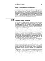
TI 8847
MIPS R3010
Figure continued on next page
A.11
Fallacies and Pitfalls
A-65
Weitek 3364
FIGURE A.37 Chip layout for the TI 8847, MIPS R3010, and Weitek 3364. In the left-hand columns are the photomicrographs; the right-hand columns show the corresponding floor plans.
A.11
Fallacies and Pitfalls
Fallacy: Underflows rarely occur in actual floating-point application code.
Although most codes rarely underflow, there are actual codes that underflow frequently. SDRWAVE [Kahaner 1988], which solves a one-dimensional wave
equation, is one such example. This program underflows quite frequently, even
when functioning properly. Measurements on one machine show that adding
hardware support for gradual underflow would cause SDRWAVE to run about
50% faster.
Fallacy: Conversions between integer and floating point are rare.
In fact, in spice they are as frequent as divides. The assumption that conversions
are rare leads to a mistake in the SPARC version 8 instruction set, which does not
provide an instruction to move from integer registers to floating-point registers.
A-66
Appendix A Computer Arithmetic
Pitfall: Don’t increase the speed of a floating-point unit without increasing its
memory bandwidth.
A typical use of a floating-point unit is to add two vectors to produce a third vector. If these vectors consist of double-precision numbers, then each floating-point
add will use three operands of 64 bits each, or 24 bytes of memory. The memory
bandwidth requirements are even greater if the floating-point unit can perform
addition and multiplication in parallel (as most do).
Pitfall: −x is not the same as 0 − x.
This is a fine point in the IEEE standard that has tripped up some designers. Because floating-point numbers use the sign/magnitude system, there are two zeros,
+0 and −0. The standard says that 0 − 0 = +0, whereas −(0) = −0. Thus −x is not
the same as 0 − x when x = 0.
A.12
Historical Perspective and References
The earliest computers used fixed point rather than floating point. In “Preliminary
Discussion of the Logical Design of an Electronic Computing Instrument,”
Burks, Goldstine, and von Neumann [1946] put it like this:
There appear to be two major purposes in a “floating” decimal point system both
of which arise from the fact that the number of digits in a word is a constant fixed
by design considerations for each particular machine. The first of these purposes
is to retain in a sum or product as many significant digits as possible and the second of these is to free the human operator from the burden of estimating and inserting into a problem “scale factors” — multiplicative constants which serve to
keep numbers within the limits of the machine.
There is, of course, no denying the fact that human time is consumed in arranging
for the introduction of suitable scale factors. We only argue that the time so consumed is a very small percentage of the total time we will spend in preparing an
interesting problem for our machine. The first advantage of the floating point is,
we feel, somewhat illusory. In order to have such a floating point, one must waste
memory capacity which could otherwise be used for carrying more digits per
word. It would therefore seem to us not at all clear whether the modest advantages
of a floating binary point offset the loss of memory capacity and the increased
complexity of the arithmetic and control circuits.
This enables us to see things from the perspective of early computer designers,
who believed that saving computer time and memory were more important than
saving programmer time.
A.12
Historical Perspective and References
A-67
The original papers introducing the Wallace tree, Booth recoding, SRT division, overlapped triplets, and so on, are reprinted in Swartzlander [1990]. A good
explanation of an early machine (the IBM 360/91) that used a pipelined Wallace
tree, Booth recoding, and iterative division is in Anderson et al. [1967]. A discussion of the average time for single-bit SRT division is in Freiman [1961]; this is
one of the few interesting historical papers that does not appear in Swartzlander.
The standard book of Mead and Conway [1980] discouraged the use of CLAs
as not being cost effective in VLSI. The important paper by Brent and Kung
[1982] helped combat that view. An example of a detailed layout for CLAs can be
found in Ngai and Irwin [1985] or in Weste and Eshraghian [1993], and a more
theoretical treatment is given by Leighton [1992]. Takagi, Yasuura, and Yajima
[1985] provide a detailed description of a signed-digit tree multiplier.
Before the ascendancy of IEEE arithmetic, many different floating-point formats were in use. Three important ones were used by the IBM/370, the DEC
VAX, and the Cray. Here is a brief summary of these older formats. The VAX format is closest to the IEEE standard. Its single-precision format (F format) is like
IEEE single precision in that it has a hidden bit, 8 bits of exponent, and 23 bits of
fraction. However, it does not have a sticky bit, which causes it to round halfway
cases up instead of to even. The VAX has a slightly different exponent range from
IEEE single: Emin is −128 rather than −126 as in IEEE, and Emax is 126 instead of
127. The main differences between VAX and IEEE are the lack of special values
and gradual underflow. The VAX has a reserved operand, but it works like a
signaling NaN: it traps whenever it is referenced. Originally, the VAX’s double
precision (D format) also had 8 bits of exponent. However, as this is too small for
many applications, a G format was added; like the IEEE standard, this format has
11 bits of exponent. The VAX also has an H format, which is 128 bits long.
The IBM/370 floating-point format uses base 16 rather than base 2. This
means it cannot use a hidden bit. In single precision, it has 7 bits of exponent and
7
24 bits (6 hex digits) of fraction. Thus, the largest representable number is 162 =
7
9
8
24 × 2 = 22 , compared with 22 for IEEE. However, a number that is normalized
in the hexadecimal sense only needs to have a nonzero leading digit. When interpreted in binary, the three most-significant bits could be zero. Thus, there are potentially fewer than 24 bits of significance. The reason for using the higher base
was to minimize the amount of shifting required when adding floating-point
numbers. However, this is less significant in current machines, where the floating-point add time is usually fixed independently of the operands. Another difference between 370 arithmetic and IEEE arithmetic is that the 370 has neither a
round digit nor a sticky digit, which effectively means that it truncates rather than
rounds. Thus, in many computations, the result will systematically be too small.
Unlike the VAX and IEEE arithmetic, every bit pattern is a valid number. Thus,
library routines must establish conventions for what to return in case of errors. In
the IBM FORTRAN library, for example, – 4 returns 2!
Arithmetic on Cray computers is interesting because it is driven by a motivation for the highest possible floating-point performance. It has a 15-bit exponent
A-68
Appendix A Computer Arithmetic
field and a 48-bit fraction field. Addition on Cray computers does not have a
guard digit, and multiplication is even less accurate than addition. Thinking of
multiplication as a sum of p numbers, each 2p bits long, Cray computers drop the
low-order bits of each summand. Thus, analyzing the exact error characteristics of
the multiply operation is not easy. Reciprocals are computed using iteration, and
division of a by b is done by multiplying a times 1/b. The errors in multiplication
and reciprocation combine to make the last three bits of a divide operation unreliable. At least Cray computers serve to keep numerical analysts on their toes!
The IEEE standardization process began in 1977, inspired mainly by W.
Kahan and based partly on Kahan’s work with the IBM 7094 at the University of
Toronto [Kahan 1968]. The standardization process was a lengthy affair, with
gradual underflow causing the most controversy. (According to Cleve Moler, visitors to the U.S. were advised that the sights not to be missed were Las Vegas, the
Grand Canyon, and the IEEE standards committee meeting.) The standard was finally approved in 1985. The Intel 8087 was the first major commercial IEEE implementation and appeared in 1981, before the standard was finalized. It contains
features that were eliminated in the final standard, such as projective bits. According to Kahan, the length of double-extended precision was based on what
could be implemented in the 8087. Although the IEEE standard was not based on
any existing floating-point system, most of its features were present in some other system. For example, the CDC 6600 reserved special bit patterns for INDEFINITE and INFINITY, while the idea of denormal numbers appears in Goldberg
[1967] as well as in Kahan [1968]. Kahan was awarded the 1989 Turing prize in
recognition of his work on floating point.
Although floating point rarely attracts the interest of the general press, newspapers were filled with stories about floating-point division in November 1994. A
bug in the division algorithm used on all of Intel’s Pentium chips had just come to
light. It was discovered by Thomas Nicely, a math professor at Lynchburg College in Virginia. Nicely found the bug when doing calculations involving reciprocals of prime numbers. News of Nicely’s discovery first appeared in the press on
the front page of the November 7 issue of Electronic Engineering Times. Intel’s
immediate response was to stonewall, asserting that the bug would only affect
theoretical mathematicians. Intel told the press, “This doesn’t even qualify as an
errata . . . even if you’re an engineer, you’re not going to see this.”
Under more pressure, Intel issued a white paper, dated November 30, explaining why they didn’t think the bug was significant. One of their arguments was
based on the fact that if you pick two floating-point numbers at random and divide one into the other, the chance that the resulting quotient will be in error is
about 1 in 9 billion. However, Intel neglected to explain why they thought that the
typical customer accessed floating-point numbers randomly.
Pressure continued to mount on Intel. One sore point was that Intel had known
about the bug before Nicely discovered it, but had decided not to make it public.
Finally, on December 20, Intel announced that they would unconditionally replace any Pentium chip that used the faulty algorithm and that they would take an
unspecified charge against earnings, which turned out to be $300 million.
A.12
Historical Perspective and References
A-69
The Pentium uses a simple version of SRT division as discussed in section
A.9. The bug was introduced when they converted the quotient lookup table to a
PLA. Evidently there were a few elements of the table containing the quotient
digit 2 that Intel thought would never be accessed, and they optimized the PLA
design using this assumption. The resulting PLA returned 0 rather than 2 in these
situations. However, those entries were really accessed, and this caused the division bug. Even though the effect of the faulty PLA was to cause 5 out of 2048 table entries to be wrong, the Pentium only computes an incorrect quotient 1 out of
9 billion times on random inputs. This is explored in Exercise A.34.
References
ANDERSON, S. F., J. G. EARLE, R. E. GOLDSCHMIDT, AND D. M. POWERS [1967]. “The IBM System/
360 Model 91: Floating-point execution unit,” IBM J. Research and Development 11, 34–53. Reprinted in Swartzlander [1990].
Good description of an early high-performance floating-point unit that used a pipelined
Wallace-tree multiplier and iterative division.
BELL, C. G. AND A. NEWELL [1971]. Computer Structures: Readings and Examples, McGraw-Hill,
New York.
BIRMAN, M., A. SAMUELS, G. CHU, T. CHUK, L. HU, J. MCLEOD, AND J. BARNES [1990]. “Developing the WRL3170/3171 SPARC floating-point coprocessors,” IEEE Micro 10:1, 55–64.
These chips have the same floating-point core as the Weitek 3364, and this paper has a fairly
detailed description of that floating-point design.
BRENT, R. P. AND H. T. KUNG [1982]. “A regular layout for parallel adders,” IEEE Trans. on Computers C-31, 260–264.
This is the paper that popularized CLAs in VLSI.
BURGESS, N. AND T. WILLIAMS [1995]. “Choices of operand truncation in the SRT division algorithm,” IEEE Trans. on Computers 44:7.
Analyzes how many bits of divisor and remainder need to be examined in SRT division.
BURKS, A. W., H. H. GOLDSTINE, AND J. VON NEUMANN [1946]. “Preliminary discussion of the logical design of an electronic computing instrument,” Report to the U.S. Army Ordnance Department,
p. 1; also appears in Papers of John von Neumann, W. Aspray and A. Burks, eds., MIT Press, Cambridge, Mass., and Tomash Publishers, Los Angeles, Calif., 1987, 97–146.
CODY, W. J., J. T. COONEN, D. M. GAY, K. HANSON, D. HOUGH, W. KAHAN, R. KARPINSKI,
J. PALMER, F. N. RIS, AND D. STEVENSON [1984]. “A proposed radix- and word-length-independent standard for floating-point arithmetic,” IEEE Micro 4:4, 86–100.
Contains a draft of the 854 standard, which is more general than 754. The significance of this
article is that it contains commentary on the standard, most of which is equally relevant to
754. However, be aware that there are some differences between this draft and the final standard.
COONEN, J. [1984]. Contributions to a Proposed Standard for Binary Floating-Point Arithmetic,
Ph.D. Thesis, Univ. of Calif., Berkeley.
The only detailed discussion of how rounding modes can be used to implement efficient binary
decimal conversion.
A-70
Appendix A Computer Arithmetic
DARLEY, H. M., ET AL. [1989]. “Floating point/integer processor with divide and square root functions,” U.S. Patent 4,878,190, October 31, 1989.
Pretty readable as patents go. Gives a high-level view of the TI 8847 chip, but doesn’t have all
the details of the division algorithm.
DEMMEL, J. W. AND X. LI [1994]. “Faster numerical algorithms via exception handling,” IEEE
Trans. on Computers 43:8, 983–992.
A good discussion of how the features unique to IEEE floating point can improve the performance of an important software library.
FREIMAN, C. V. [1961]. “Statistical analysis of certain binary division algorithms,” Proc. IRE 49:1,
91–103.
Contains an analysis of the performance of shifting-over-zeros SRT division algorithm.
GOLDBERG, D. [1991]. “What every computer scientist should know about floating-point arithmetic,”
Computing Surveys 23:1, 5–48.
Contains an in-depth tutorial on the IEEE standard from the software point of view.
GOLDBERG, I. B. [1967]. “27 bits are not enough for 8-digit accuracy,” Comm. ACM 10:2, 105–106.
This paper proposes using hidden bits and gradual underflow.
GOSLING, J. B. [1980]. Design of Arithmetic Units for Digital Computers, Springer-Verlag, New
York.
A concise, well-written book, although it focuses on MSI designs.
HAMACHER, V. C., Z. G. VRANESIC, AND S. G. ZAKY [1984]. Computer Organization, 2nd ed.,
McGraw-Hill, New York.
Introductory computer architecture book with a good chapter on computer arithmetic.
HWANG, K. [1979]. Computer Arithmetic: Principles, Architecture, and Design, Wiley, New York.
This book contains the widest range of topics of the computer arithmetic books.
IEEE [1985]. “IEEE standard for binary floating-point arithmetic,” SIGPLAN Notices 22:2, 9–25.
IEEE 754 is reprinted here.
KAHAN, W. [1968]. “7094-II system support for numerical analysis,” SHARE Secretarial Distribution SSD-159.
This system had many features that were incorporated into the IEEE floating-point standard.
KAHANER, D. K. [1988]. “Benchmarks for ‘real’ programs,” SIAM News (November).
The benchmark presented in this article turns out to cause many underflows.
KNUTH, D. [1981]. The Art of Computer Programming, vol. II, 2nd ed., Addison-Wesley, Reading,
Mass.
Has a section on the distribution of floating-point numbers.
KOGGE, P. [1981]. The Architecture of Pipelined Computers, McGraw-Hill, New York.
Has brief discussion of pipelined multipliers.
KOHN, L. AND S.-W. FU [1989]. “A 1,000,000 transistor microprocessor,” IEEE Int’l Solid-State Circuits Conf., 54–55.
There are several articles about the i860, but this one contains the most details about its floating-point algorithms.
KOREN, I. [1989]. Computer Arithmetic Algorithms, Prentice Hall, Englewood Cliffs, N.J.
LEIGHTON, F. T. [1992]. Introduction to Parallel Algorithms and Architectures: Arrays, Trees, Hypercubes, Morgan Kaufmann, San Mateo, Calif.
This is an excellent book, with emphasis on the complexity analysis of algorithms.
Section 1.2.1 has a nice discussion of carry-lookahead addition on a tree.
A.12
Historical Perspective and References
A-71
MAGENHEIMER, D. J., L. PETERS, K. W. PETTIS, AND D. ZURAS [1988]. “Integer multiplication and
division on the HP Precision architecture,” IEEE Trans. on Computers 37:8, 980–990.
Gives rationale for the integer- and divide-step instructions in the Precision architecture.
MARKSTEIN, P. W. [1990]. “Computation of elementary functions on the IBM RISC System/6000
processor,” IBM J. of Research and Development 34:1, 111–119.
Explains how to use fused muliply-add to compute correctly rounded division and square
root.
MEAD, C. AND L. CONWAY [1980]. Introduction to VLSI Systems, Addison-Wesley, Reading, Mass.
MONTOYE, R. K., E. HOKENEK, AND S. L. RUNYON [1990]. “Design of the IBM RISC System/6000
floating-point execution,” IBM J. of Research and Development 34:1, 59–70.
Describes one implementation of fused multiply-add.
NGAI, T.-F. AND M. J. IRWIN [1985]. “Regular, area-time efficient carry-lookahead adders,” Proc.
Seventh IEEE Symposium on Computer Arithmetic, 9–15.
Describes a CLA like that of Figure A.17, where the bits flow up and then come back down.
PATTERSON, D.A. AND J.L. HENNESSY [1994]. Computer Organization and Design: The Hardware/
Software Interface, Morgan Kaufmann, San Francisco.
Chapter 4 is a gentler introduction to the first third of this appendix.
PENG, V., S. SAMUDRALA, AND M. GAVRIELOV [1987]. “On the implementation of shifters, multipliers, and dividers in VLSI floating point units,” Proc. Eighth IEEE Symposium on Computer Arithmetic, 95–102.
Highly recommended survey of different techniques actually used in VLSI designs.
ROWEN, C., M. JOHNSON, AND P. RIES [1988]. “The MIPS R3010 floating-point coprocessor,” IEEE
Micro 53–62 (June).
SANTORO, M. R., G. BEWICK, AND M. A. HOROWITZ [1989]. “Rounding algorithms for IEEE multipliers,” Proc. Ninth IEEE Symposium on Computer Arithmetic, 176–183.
A very readable discussion of how to efficiently implement rounding for floating-point multiplication.
SCOTT, N. R. [1985]. Computer Number Systems and Arithmetic, Prentice Hall, Englewood Cliffs,
N.J.
SWARTZLANDER, E., ED. [1990]. Computer Arithmetic, IEEE Computer Society Press, Los Alamitos,
Calif.
A collection of historical papers in two volumes.
TAKAGI, N., H. YASUURA, AND S. YAJIMA [1985].“High-speed VLSI multiplication algorithm with a
redundant binary addition tree,” IEEE Trans. on Computers C-34:9, 789–796.
A discussion of the binary-tree signed multiplier that was the basis for the design used in the
TI 8847.
TAYLOR, G. S. [1981]. “Compatible hardware for division and square root,” Proc. Fifth IEEE Symposium on Computer Arithmetic, 127–134.
Good discussion of a radix-4 SRT division algorithm.
TAYLOR, G. S. [1985]. “Radix 16 SRT dividers with overlapped quotient selection stages,” Proc. Seventh IEEE Symposium on Computer Arithmetic, 64–71.
Describes a very sophisticated high-radix division algorithm.
WESTE, N. AND K. ESHRAGHIAN [1993]. Principles of CMOS VLSI Design: A Systems Perspective,
2nd ed., Addison-Wesley, Reading, Mass.
This textbook has a section on the layouts of various kinds of adders.
A-72
Appendix A Computer Arithmetic
WILLIAMS, T. E., M. HOROWITZ, R. L. ALVERSON, AND T. S. YANG [1987]. “A self-timed chip for division,” Advanced Research in VLSI, Proc. 1987 Stanford Conf., MIT Press, Cambridge, Mass.
Describes a divider that tries to get the speed of a combinational design without using the
area that would be required by one.
E X E R C I S E S
A.1 [12] <A.2> Using n bits, what is the largest and smallest integer that can be represented in the two’s complement system?
A.2 [20/25] <A.2> In the subsection Signed Numbers (page A-7), it was stated that two’s
complement overflows when the carry into the high-order bit position is different from the
carry-out from that position.
a.
[20] <A.2> Give examples of pairs of integers for all four combinations of carry-in
and carry-out. Verify the rule stated above.
b.
[25] <A.2> Explain why the rule is always true.
A.3 [12] <A.2> Using 4-bit binary numbers, multiply −8 × −8 using Booth recoding.
A.4 [15] <A.2> Equations A.2.1 and A.2.2 are for adding two n-bit numbers. Derive similar equations for subtraction, where there will be a borrow instead of a carry.
A.5 [25] <A.2> On a machine that doesn’t detect integer overflow in hardware, show how
you would detect overflow on a signed addition operation in software.
A.6 [15/15/20] <A.3> Represent the following numbers as single-precision and doubleprecision IEEE floating-point numbers.
a.
[15] <A.3> 10.
b.
[15] <A.3> 10.5.
c.
[20] <A.3> 0.1.
A.7 [12/12/12/12/12] <A.3> Below is a list of floating-point numbers. In single precision,
write down each number in binary, in decimal, and give its representation in IEEE arithmetic.
a.
[12] <A.3> The largest number less than 1.
b.
[12] <A.3> The largest number.
c.
[12] <A.3> The smallest positive normalized number.
d.
[12] <A.3> The largest denormal number.
e.
[12] <A.3> The smallest positive number.
A.8 [15] <A.3> Is the ordering of nonnegative floating-point numbers the same as integers
when denormalized numbers are also considered?
A.9 [20] <A.3> Write a program that prints out the bit patterns used to represent floatingpoint numbers on your favorite computer. What bit pattern is used for NaN?
Exercises
A-73
A.10 [15] <A.4> Using p = 4, show how the binary floating-point multiply algorithm computes the product of 1.875 × 1.875.
A.11 [12/10] <A.4> Concerning the addition of exponents in floating-point multiply:
a.
[12] <A.4> What would the hardware that implements the addition of exponents look
like?
b.
[10] <A.4> If the bias in single precision were 129 instead of 127, would addition be
harder or easier to implement?
A.12 [15/12] <A.4> In the discussion of overflow detection for floating-point multiplication, it was stated that (for single precision) you can detect an overflowed exponent by performing exponent addition in a 9-bit adder.
a.
[15] <A.4> Give the exact rule for detecting overflow.
b.
[12] <A.4> Would overflow detection be any easier if you used a 10-bit adder instead?
A.13 [15/10] <A.4> Floating-point multiplication:
a.
[15] <A.4> Construct two single-precision floating-point numbers whose product
doesn’t overflow until the final rounding step.
b.
[10] <A.4> Is there any rounding mode where this phenomenon cannot occur?
A.14 [15] <A.4> Give an example of a product with a denormal operand but a normalized
output. How large was the final shifting step? What is the maximum possible shift that can
occur when the inputs are double-precision numbers?
A.15 [15] <A.5> Use the floating-point addition algorithm on page A-24 to compute
1.0102 − .10012 (in 4-bit precision) .
A.16 [10/15/20/20/20] <A.5> In certain situations, you can be sure that a + b is exactly representable as a floating-point number, that is, no rounding is necessary.
a.
[10] <A.5> If a, b have the same exponent and different signs, explain why a + b is
exact. This was used in the subsection Speeding Up Addition on page A-27.
b.
[15] <A.5> Give an example where the exponents differ by 1, a and b have different
signs, and a + b is not exact.
c.
[20] <A.5> If a ≥ b ≥ 0, and the top two bits of a cancel when computing a − b, explain
why the result is exact (this fact is mentioned on page A-23).
d.
[20] <A.5> If a ≥ b ≥ 0, and the exponents differ by 1, show that a − b is exact unless
the high order bit of a − b is in the same position as that of a (mentioned in Speeding
Up Addition, page A-27).
e.
[20] <A.5> If the result of a − b or a + b is denormal, show that the result is exact (mentioned in the subsection Underflow, page A-38).
A.17 [15/20] <A.5> Fast floating-point addition (using parallel adders) for p = 5.
a.
[15] <A.5> Step through the fast addition algorithm for a + b, where a = 1.01112 and
b = .110112.
A-74
Appendix A Computer Arithmetic
b.
[20] <A.5> Suppose the rounding mode is toward +∞. What complication arises in the
above example for the adder that assumes a carry-out? Suggest a solution.
A.18 [12] <A.4,A.5> How would you use two parallel adders to avoid the final round-up
addition in floating-point multiplication?
A.19 [30/10] <A.5> This problem presents a way to reduce the number of addition steps
in floating-point addition from three to two using only a single adder.
a.
[30] <A.5> Let A and B be integers of opposite signs, with a and b be their magnitudes. Show that the following rules for manipulating the unsigned numbers a and b
gives A + B.
1.
2.
Using end around carry to add the complemented operand and the other (uncomplemented) one.
3.
If there was a carry-out, the sign of the result is the sign associated with the uncomplemented operand.
4.
b.
Complement one of the operands.
Otherwise, if there was no carry-out, complement the result, and give it the sign
of the complemented operand.
[10] <A.5> Use the above to show how steps 2 and 4 in the floating-point addition algorithm can be performed using only a single addition.
A.20 [20/15/20/15/20/15] <A.6> Iterative square root.
a.
[20] <A.6> Use Newton’s method to derive an iterative algorithm for square root. The
formula will involve a division.
b.
[15] <A.6> What is the fastest way you can think of to divide a floating-point number
by 2?
c.
[20] <A.6> If division is slow, then the iterative square root routine will also be slow.
Use Newton’s method on f(x) = 1/x2 − a to derive a method that doesn’t use any divisions.
d.
[15] <A.6> Assume that the ratio division by 2 : floating-point add : floating-point
multiply is 1:2:4. What ratios of multiplication time to divide time makes each iteration step in the method of part(c) faster than each iteration in the method of part(a)?
e.
[20] <A.6> When using the method of part(a), how many bits need to be in the initial
guess in order to get double-precision accuracy after three iterations? (You may ignore
rounding error.)
f.
[15] <A.6> Suppose that when Spice runs on the TI 8847, it spends 16.7% of its time
in the square root routine (this percentage has been measured on other machines). Using the values in Figure A.36 and assuming three iterations, how much slower would
Spice run if square root was implemented in software using the method of part(a)?
A.21 [10/20/15/15/15] <A.6> Correctly rounded iterative division. Let a and b be floatingpoint numbers with p-bit significands (p = 53 in double precision). Let q be the exact quotient q = a/b, 1 ≤ q < 2. Suppose that q is the result of an iteration process, that q has a few
Exercises
A-75
extra bits of precision, and that 0 < q − q < 2−p . For the following, it is important that
q < q, even when q can be exactly represented as a floating-point number.
a.
[10] <A.6> If x is a floating-point number, and 1 ≤ x < 2, what is the next representable
number after x?
b.
[20] <A.6> Show how to compute q′ from q, where q′ has p + 1 bits of precision and
−p
q − q′ < 2 .
c.
[15] <A.6> Assuming round to nearest, show that the correctly rounded quotient is
either q′, q′ − 2−p, or q′ + 2−p.
d.
[15] <A.6> Give rules for computing the correctly rounded quotient from q′ based on
the low-order bit of q′ and the sign of a − bq′.
e.
[15] <A.6> Solve part(c) for the other three rounding modes.
A.22 [15] <A.6> Verify the formula on page A-31. [Hint: If xn = x0(2 − x0b) × Πi=1, n [1 +
i
i
(1 − x0b)2 ], then 2 − xnb = 2 − x0b(2 − x0b) Π[1 + (1 − x0b)2 ] = 2 − [1 − (1 − x0b)2] Π[1
i
+ (1 − x0b)2 ].]
A.23 [15] <A.7> Our example that showed that double rounding can give a different answer from rounding once used the round-to-even rule. If halfway cases are always rounded
up, is double rounding still dangerous?
A.24 [10/10/20/20] <A.7> Some of the cases of the italicized statement in the Precisions
subsection (page A-34) aren’t hard to demonstrate.
a.
[10] <A.7> What form must a binary number have if rounding to q bits followed by
rounding to p bits gives a different answer than rounding directly to p bits?
b.
[10] <A.7> Show that for multiplication of p-bit numbers, rounding to q bits followed
by rounding to p bits is the same as rounding immediately to p bits if q ≥ 2p.
c.
[20] <A.7> If a and b are p-bit numbers with the same sign, show that rounding a + b
to q bits followed by a rounding to p bits is the same as rounding immediately to p bits
if q ≥ 2p + 1.
d.
[20] <A.7> Do part (c) when a and b have opposite signs.
A.25 [Discussion] <A.7> In the MIPS approach to exception handling, you need a test for
determining whether two floating-point operands could cause an exception. This should be
fast and also not have too many false positives. Can you come up with a practical test? The
performance cost of your design will depend on the distribution of floating-point numbers.
This is discussed in Knuth [1981] and the Hamming paper in Swartzlander [1990].
A.26 [12/12/10] <A.8> Carry-skip adders.
a.
[12] <A.8> Assuming that time is proportional to logic levels, how long does it take
an n-bit adder divided into (fixed) blocks of length k bits to perform an addition?
b.
[12] <A.8> What value of k gives the fastest adder?
c.
[10] <A.8> Explain why the carry-skip adder takes time 0 ( n ).
A-76
Appendix A Computer Arithmetic
A.27 [10/15/20] <A.8> Complete the details of the block diagrams for the following
adders.
a.
[10] <A.8> In Figure A.15, show how to implement the “1” and “2” boxes in terms of
AND and OR gates.
b.
[15] <A.8> In Figure A.18, what signals need to flow from the adder cells in the top
row into the “C” cells? Write the logic equations for the “C” box.
c.
[20] <A.8> Show how to extend the block diagram in A.17 so it will produce the
carry-out bit c8.
A.28 [15] <A.9> For ordinary Booth recoding, the multiple of b used in the ith step is
simply ai–1 − ai. Can you find a similar formula for radix-4 Booth recoding (overlapped
triplets)?
A.29 [20] <A.9> Expand Figure A.29 in the fashion of A.27, showing the individual
adders.
A.30 [25] <A.9> Write out the analogue of Figure A.25 for radix-8 Booth recoding.
A.31 [18] <A.9> Suppose that an–1. . .a1a0 and bn–1. . .b1b0 are being added in a signed-digit
adder as illustrated in the Example on page A-56. Write a formula for the ith bit of the sum,
si, in terms of ai, ai–1, ai–2, bi, bi–1, and bi–2.
A.32 [15] <A.9> The text discussed radix-4 SRT division with quotient digits of −2, −1, 0,
1, 2. Suppose that 3 and −3 are also allowed as quotient digits. What relation replaces ri
≤ 2b/3?
A.33 [25/20/30] <A.9> Concerning the SRT division table, Figure A.34:
a.
[25] <A.9> Write a program to generate the results of Figure A.34.
b.
[20] <A.9> Note that Figure A.34 has a certain symmetry with respect to positive and
negative values of P. Can you find a way to exploit the symmetry and only store the
values for positive P?
c.
[30] <A.9> Suppose a carry-save adder is used instead of a propagate adder. The input
to the quotient lookup table will be k bits of divisor, and l bits of remainder, where the
remainder bits are computed by summing the top l bits of the sum and carry registers.
What are k and l? Write a program to generate the analogue of Figure A.34.
A.34 [12/12/12]<A.9,A.12>The first several million Pentium chips produced had a flaw
that caused division to sometimes return the wrong result. The Pentium uses a radix-4 SRT
algorithm similar to the one illustrated in the Example on page A-59 (but with the remainder stored in carry-save format: see Exercise A.33(c)). According to Intel, the bug was due
to five incorrect entries in the quotient lookup table.
a.
[12] <A.9,A.12> The bad entries should have had a quotient of plus or minus 2, but
instead had a quotient of 0. Because of redundancy, it’s conceivable that the algorithm
could “recover” from a bad quotient digit on later iterations. Show that this is not possible for the Pentium flaw.
Exercises
A-77
b.
[12] <A.9,A.12> Since the operation is a floating-point divide rather than an integer
divide, the SRT division algorithm on page A-47 must be modified in two ways. First,
step 1 is no longer needed, since the divisor is already normalized. Second, the very
first remainder may not satisfy the proper bound (r ≤ 2b/3 for Pentium, see page A58). Show that skipping the very first left shift in step 2(a) of the SRT algorithm will
solve this problem.
c.
[12] <A.9,A.12> If the faulty table entries were indexed by a remainder that could occur at the very first divide step (when the remainder is the divisor), random testing
would quickly reveal the bug. This didn’t happen. What does that tell you about the
remainder values that index the faulty entries?
A.35 [12/12/12] <A.6,A.9> The discussion of the remainder-step instruction assumed that
division was done using a bit-at-a-time algorithm. What would have to change if division
were implemented using a higher-radix method?
A.36 [25] <A.9> In the array of Figure A.28, the fact that an array can be pipelined is not
exploited. Can you come up with a design that feeds the output of the bottom CSA into the
bottom CSAs instead of the top one, and that will run faster than the arrangement of
Figure A.28?
B
Vector Processors
I’m certainly not inventing vector processors. There are three
kinds that I know of existing today. They are represented by the
Illiac-IV, the (CDC) Star processor, and the TI (ASC) processor.
Those three were all pioneering processors.... One of the problems
of being a pioneer is you always make mistakes and I never, never
want to be a pioneer. It’salways best to come second when you can
look at the mistakes the pioneers made.
Seymour Cray
Public Lecture at Lawrence Livermore Laboratories
on the Introduction of the CRAY-1 (1976)
2
B.1
Why Vector Processors?
B-1
B.2
Basic Vector Architecture
B-3
B.3
Two Real-World Issues: Vector Length and Stride
B-15
B.4
Effectiveness of Compiler Vectorization
B-22
B.5
Enhancing Vector Performance
B-23
B.6
Putting It All Together: Performance of Vector Processors
B-29
B.7
Fallacies and Pitfalls
B-35
B.8
Concluding Remarks
B-37
B.9
Historical Perspective and References
B-38
Exercises
B-43
B.1
Why Vector Processors?
In Chapters 3 and 4 we looked at pipelining and exploitation of instruction-level
parallelism in detail and saw that pipeline scheduling, issuing multiple instructions per clock cycle, and more deeply pipelining a processor could significantly
improve the performance of a processor. (This appendix assumes that you have
read Chapter 3 completely and at least skimmed Chapter 4; in addition, the discussion on vector memory systems assumes that you have read Chapter 5.) Yet
there are limits on the performance improvement that pipelining can achieve.
These limits are set by two primary factors:
s
s
Clock cycle time—The clock cycle time can be decreased by making the pipelines deeper, but a deeper pipeline will increase the pipeline dependences and
result in a higher CPI. At some point, each increase in pipeline depth has a corresponding increase in CPI. As we saw in Chapter 3’s Fallacies and Pitfalls,
very deep pipelining can slow down a processor.
Instruction fetch and decode rate—This obstacle, sometimes called the Flynn
bottleneck (based on Flynn [1966]), makes it difficult to fetch and issue many
B-2
Appendix B Vector Processors
instructions per clock. This obstacle is one reason that it has been difficult to
build processors with high clock rates and very high issue rates.
The dual limitations imposed by deeper pipelines and issuing multiple instructions can be viewed from the standpoint of either clock rate or CPI: It is just as
difficult to schedule a pipeline that is n times deeper as it is to schedule a processor that issues n instructions per clock cycle.
High-speed, pipelined processors are particularly useful for large scientific
and engineering applications. A high-speed pipelined processor will usually use a
cache to avoid forcing memory reference instructions to have very long latency.
Unfortunately, big, long-running, scientific programs often have very large active
data sets that are sometimes accessed with low locality, yielding poor performance from the memory hierarchy. This problem could be overcome by not caching these structures if it were possible to determine the memory-access patterns
and pipeline the memory accesses efficiently. Novel cache architectures and compiler assistance through blocking and prefetching are decreasing these memory
hierarchy problems, but they continue to be serious in some applications.
Vector processors provide high-level operations that work on vectors—linear
arrays of numbers. A typical vector operation might add two 64-element, floatingpoint vectors to obtain a single 64-element vector result. The vector instruction is
equivalent to an entire loop, with each iteration computing one of the 64 elements
of the result, updating the indices, and branching back to the beginning.
Vector instructions have several important properties that solve most of the
problems mentioned above:
s
s
s
s
The computation of each result is independent of the computation of previous
results, allowing a very deep pipeline without generating any data hazards. Essentially, the absence of data hazards was determined by the compiler or by the
programmer when she decided that a vector instruction could be used.
A single vector instruction specifies a great deal of work—it is equivalent to executing an entire loop. Thus, the instruction bandwidth requirement is reduced,
and the Flynn bottleneck is considerably mitigated.
Vector instructions that access memory have a known access pattern. If the vector’s elements are all adjacent, then fetching the vector from a set of heavily interleaved memory banks works very well (as we saw in section 5.6). The high
latency of initiating a main memory access versus accessing a cache is amortized, because a single access is initiated for the entire vector rather than to a
single word. Thus, the cost of the latency to main memory is seen only once for
the entire vector, rather than once for each word of the vector.
Because an entire loop is replaced by a vector instruction whose behavior is
predetermined, control hazards that would normally arise from the loop branch
are nonexistent.
B.2
Basic Vector Architecture
B-3
For these reasons, vector operations can be made faster than a sequence of scalar
operations on the same number of data items, and designers are motivated to include vector units if the applications domain can use them frequently.
As mentioned above, vector processors pipeline the operations on the individual elements of a vector. The pipeline includes not only the arithmetic operations
(multiplication, addition, and so on), but also memory accesses and effective address calculations. In addition, most high-end vector processors allow multiple
vector operations to be done at the same time, creating parallelism among the operations on different elements. In this appendix, we focus on vector processors
that gain performance by pipelining and instruction overlap.
B.2
Basic Vector Architecture
A vector processor typically consists of an ordinary pipelined scalar unit plus a
vector unit. All functional units within the vector unit have a latency of several
clock cycles. This allows a shorter clock cycle time and is compatible with longrunning vector operations that can be deeply pipelined without generating hazards. Most vector processors allow the vectors to be dealt with as floating-point
numbers, as integers, or as logical data. Here we will focus on floating point. The
scalar unit is basically no different from the type of advanced pipelined CPU discussed in Chapter 3.
There are two primary types of architectures for vector processors: vectorregister processors and memory-memory vector processors. In a vector-register
processor, all vector operations—except load and store—are among the vector
registers. These architectures are the vector counterpart of a load-store architecture. All major vector computers shipped since the late 1980s use a vector-register
architecture; these include the Cray Research processors (CRAY-1, CRAY-2, XMP, Y-MP, and C-90), the Japanese supercomputers (NEC SX/2 and SX/3, Fujitsu
VP200 and VP400, and the Hitachi S820), as well as the mini-supercomputers
(Convex C-1 and C-2). In a memory-memory vector processor, all vector operations are memory to memory. The first vector computers were of this type, as were
CDC’s vector computers. From this point on we will focus on vector-register architectures only; we will briefly return to memory-memory vector architectures at
the end of the appendix (section B.7) to discuss why they have not been as successful as vector-register architectures.
We begin with a vector-register processor consisting of the primary components shown in Figure B.1. This processor, which is loosely based on the
CRAY-1, is the foundation for discussion throughout most of this appendix. We
will call it DLXV; its integer portion is DLX, and its vector portion is the logical
vector extension of DLX. The rest of this section examines how the basic architecture of DLXV relates to other processors.
B-4
Appendix B Vector Processors
Main memory
Vector
load-store
FP add/subtract
FP multiply
FP divide
Vector
registers
Integer
Logical
Scalar
registers
FIGURE B.1 The basic structure of a vector-register architecture, DLXV. This processor has a scalar architecture just like DLX. There are also eight 64-element vector registers,
and all the functional units are vector functional units. Special vector instructions are defined
both for arithmetic and for memory accesses. We show vector units for logical and integer
operations. These are included so that DLXV looks like a standard vector processor, which
usually includes these units. However, we will not be discussing these units except in the
Exercises. The vector and scalar registers have a significant number of read and write ports
to allow multiple simultaneous vector operations. These ports are connected to the inputs and
outputs of the vector functional units by a set of crossbars (shown in thick gray lines). In
section B.5 we add chaining, which will require additional interconnect capability.
The primary components of the instruction set architecture of DLXV are
s
Vector registers—Each vector register is a fixed-length bank holding a single
vector. DLXV has eight vector registers, and each vector register holds 64 elements. Each vector register must have at least two read ports and one write
port in DLXV. This will allow a high degree of overlap among vector operations to different vector registers. (We do not consider the problem of a shortage of vector register ports. In real machines this would result in a structural
hazard.) The read and write ports, which total at least 16 read ports and eight
write ports, are connected to the functional unit inputs or outputs by a pair of
crossbars. (The CRAY-1 manages to implement the register file with only a
single port per register using some clever implementation techniques.)
B.2
s
s
s
Basic Vector Architecture
B-5
Vector functional units—Each unit is fully pipelined and can start a new operation on every clock cycle. A control unit is needed to detect hazards, both from
conflicts for the functional units (structural hazards) and from conflicts for register accesses (data hazards). DLXV has five functional units, as shown in
Figure B.1. For simplicity, we will focus exclusively on the floating-point functional units. Depending on the vector processor, scalar operations either use the
vector functional units or use a dedicated set. We assume the functional units
are shared, but again, for simplicity, we ignore potential conflicts.
Vector load-store unit—This is a vector memory unit that loads or stores a vector to or from memory. The DLXV vector loads and stores are fully pipelined,
so that words can be moved between the vector registers and memory with a
bandwidth of one word per clock cycle, after an initial latency. This unit would
also normally handle scalar loads and stores.
A set of scalar registers—Scalar registers can also provide data as input to the
vector functional units, as well as compute addresses to pass to the vector loadstore unit. These are the normal 32 general-purpose registers and 32 floatingpoint registers of DLX, though more read and write ports are needed. The scalar registers are also connected to the functional units by the pair of crossbars.
Figure B.2 shows the characteristics of some typical vector processors, including the size and count of the registers, the number and types of functional units,
and the number of load-store units.
In DLXV, vector operations use the same names as DLX operations, but with
the letter “V” appended. These are double-precision, floating-point vector operations. (We have omitted single-precision FP operations and integer and logical
operations for simplicity.) Thus, ADDV is an add of two double-precision vectors.
The vector instructions take as their input either a pair of vector registers (ADDV)
or a vector register and a scalar register, designated by appending “SV” (ADDSV).
In the latter case, the value in the scalar register is used as the input for all operations—the operation ADDSV will add the contents of a scalar register to each element in a vector register. Most vector operations have a vector destination
register, though a few (population count) produce a scalar value, which is stored
to a scalar register. The names LV and SV denote vector load and vector store, and
they load or store an entire vector of double-precision data. One operand is
the vector register to be loaded or stored; the other operand, which is a DLX
general-purpose register, is the starting address of the vector in memory.
Figure B.3 lists the DLXV vector instructions. In addition to the vector registers,
we need two additional special-purpose registers: the vector-length and vectormask registers. We will discuss these registers and their purpose in sections B.3
and B.5, respectively.
B-6
Appendix B Vector Processors
Processor
Year
announced
Clock
rate
(MHz)
Registers
Elements per
register (64-bit
elements)
CRAY-1
1976
80
8
64
6: add, multiply, reciprocal,
integer add, logical, shift
CRAY X-MP
CRAY Y-MP
1983
1988
120
166
8
64
8: FP add, FP multiply, FP reciprocal, integer add, 2 logical,
shift, population count/parity
2 loads
1 store
CRAY-2
1985
166
8
64
5: FP add, FP multiply, FP reciprocal/sqrt, integer (add shift,
population count), logical
1
Fujitsu
VP100/200
1982
133
8–256
32–1024
3: FP or integer add/logical,
multiply, divide
2
Hitachi
S810/820
1983
71
32
256
4: 2 integer add/logical,
1 multiply-add, and 1 multiply/
divide–add unit
4
Convex C-1
1985
10
8
128
4: multiply, add, divide, integer/
logical
1
NEC SX/2
1984
160
8 + 8192
256 variable
16: 4 integer add/logical, 4 FP
multiply/divide, 4 FP add,
4 shift
8
DLXV
1990
200
8
64
5: multiply, divide, add,
integer add, logical
1
Cray C-90
1991
240
8
128
8: FP add, FP multiply, FP reciprocal, integer add, 2 logical,
shift, population count/parity
4
Convex C-4
1994
135
16
128
3: each is full integer, logical,
and FP (including multiply-add)
NEC SX/4
1995
400
8 + 8192
256 variable
16: 4 integer add/logical, 4 FP
multiply/divide, 4 FP add,
4 shift
Cray J-90
1995
100
8
64
4: FP add, FP multiply, FP reciprocal, integer/logical
Cray T-90
1996
~500
8
128
8: FP add, FP multiply, FP reciprocal, integer add, 2 logical,
shift, population count/parity
Functional units
Load-store
units
1
8
4
FIGURE B.2 Characteristics of several vector-register architectures. The vector functional units include all operation
units used by the vector instructions. The functional units are floating point unless stated otherwise. If the processor is a
multiprocessor, the entries correspond to the characteristics of one processor. Each vector load-store unit represents the
ability to do an independent, overlapped transfer to or from the vector registers. The Fujitsu VP200’s vector registers are
configurable: The size and count of the 8 K 64-bit entries may be varied inversely to one another (e.g., eight registers each
1 K elements long, or 128 registers each 64 elements long). The NEC SX/2 has eight fixed registers of length 256, plus 8 K
of configurable 64-bit registers. The reciprocal unit on the CRAY processors is used to do division (and square root on the
CRAY-2). Add pipelines perform floating-point add and subtract. The multiply/divide–add unit on the Hitachi S810/820 performs an FP multiply or divide followed by an add or subtract (while the multiply-add unit performs a multiply followed by an
add or subtract). Note that most processors use the vector FP multiply and divide units for vector integer multiply and divide,
just like DLX, and several of the processors use the same units for FP scalar and FP vector operations. Several of the
machines have different clock rates in the vector and scalar units; the clock rates shown are for the vector units.
B.2
Basic Vector Architecture
B-7
Instruction
Operands
Function
ADDV
ADDSV
V1,V2,V3
V1,F0,V2
Add elements of V2 and V3, then put each result in V1.
Add F0 to each element of V2, then put each result in V1.
SUBV
SUBVS
SUBSV
V1,V2,V3
V1,V2,F0
V1,F0,V2
Subtract elements of V3 from V2, then put each result in V1.
Subtract F0 from elements of V2, then put each result in V1.
Subtract elements of V2 from F0, then put each result in V1.
MULTV
MULTSV
V1,V2,V3
V1,F0,V2
Multiply elements of V2 and V3, then put each result in V1.
Multiply F0 by each element of V2, then put each result in V1.
DIVV
DIVVS
DIVSV
V1,V2,V3
V1,V2,F0
V1,F0,V2
Divide elements of V2 by V3, then put each result in V1.
Divide elements of V2 by F0, then put each result in V1.
Divide F0 by elements of V2, then put each result in V1.
LV
V1,R1
Load vector register V1 from memory starting at address R1.
SV
R1,V1
Store vector register V1 into memory starting at address R1.
LVWS
V1,(R1,R2)
Load V1 from address at R1 with stride in R2, i.e., R1+i × R2.
SVWS
(R1,R2),V1
Store V1 from address at R1 with stride in R2, i.e., R1+i × R2.
LVI
V1,(R1+V2)
Load V1 with vector whose elements are at R1+V2(i), i.e., V2 is an index.
SVI
(R1+V2),V1
Store V1 to vector whose elements are at R1+V2(i), i.e., V2 is an index.
CVI
V1,R1
Create an index vector by storing the values 0, 1 × R1, 2 × R1,...,63 × R1
into V1.
S--V
S--SV
V1,V2
F0,V1
Compare the elements (EQ, NE, GT, LT, GE, LE) in V1 and V2. If condition is true,
put a 1 in the corresponding bit vector; otherwise put 0. Put resulting bit vector in
vector-mask register (VM). The instruction S--SV performs the same compare but
using a scalar value as one operand.
POP
R1,VM
Count the 1s in the vector-mask register and store count in R1.
Set the vector-mask register to all 1s.
CVM
MOVI2S
MOVS2I
VLR,R1
R1,VLR
Move contents of R1 to the vector-length register.
Move the contents of the vector-length register to R1.
MOVF2S
MOVS2F
VM,F0
F0,VM
Move contents of F0 to the vector-mask register.
Move contents of vector-mask register to F0.
FIGURE B.3 The DLXV vector instructions. Only the double-precision FP operations are shown. In addition to the vector
registers, there are two special registers, VLR (discussed in section B.3) and VM (discussed in section B.5). The operations
with stride are explained in section B.3, and the use of the index creation and indexed load-store operations are explained
in section B.5.
A vector processor is best understood by looking at a vector loop on DLXV.
Let’s take a typical vector problem, which will be used throughout this appendix:
Y=a×X+Y
X and Y are vectors, initially resident in memory, and a is a scalar. This is the socalled SAXPY or DAXPY loop that forms the inner loop of the Linpack benchmark. (SAXPY stands for single-precision a × X plus Y; DAXPY for doubleprecision a × X plus Y.) Linpack is a collection of linear algebra routines, and the
B-8
Appendix B Vector Processors
routines for performing Gaussian elimination constitute what is known as the
Linpack benchmark. The DAXPY routine, which implements the above loop,
represents a small fraction of the source code of the Linpack benchmark, but it
accounts for most of the execution time for the benchmark.
For now, let us assume that the number of elements, or length, of a vector register (64) matches the length of the vector operation we are interested in. (This restriction will be lifted shortly.)
EXAMPLE
ANSWER
Show the code for DLX and DLXV for the DAXPY loop. Assume that the
starting addresses of X and Y are in Rx and Ry, respectively.
Here is the DLX code.
LD
ADDI
Loop: LD
MULTD
LD
ADDD
SD
ADDI
ADDI
SUB
BNEZ
F0,a
R4,Rx,#512
F2,0(Rx)
F2,F0,F2
F4,0(Ry)
F4,F2,F4
0(Ry),F4
Rx,Rx,#8
Ry,Ry,#8
R20,R4,Rx
R20,Loop
;last address to load
;load X(i)
;a × X(i)
;load Y(i)
;a × X(i) + Y(i)
;store into Y(i)
;increment index to X
;increment index to Y
;compute bound
;check if done
Here is the code for DLXV for DAXPY.
LD
LV
MULTSV
LV
ADDV
SV
F0,a
V1,Rx
V2,F0,V1
V3,Ry
V4,V2,V3
Ry,V4
;load scalar a
;load vector X
;vector-scalar multiply
;load vector Y
;add
;store the result
There are some interesting comparisons between the two code segments
in this Example. The most dramatic is that the vector processor greatly reduces the dynamic instruction bandwidth, executing only six instructions
versus almost 600 for DLX. This reduction occurs both because the vector
operations work on 64 elements and because the overhead instructions
that constitute nearly half the loop on DLX are not present in the DLXV
code.
s