Data Sheet High-Performance, Enhanced Flash Microcontrollers phần 4 docx
Bạn đang xem bản rút gọn của tài liệu. Xem và tải ngay bản đầy đủ của tài liệu tại đây (316.34 KB, 38 trang )
© 2006 Microchip Technology Inc. DS39564C-page 97
PIC18FXX2
9.5 PORTE, TRISE and LATE
Registers
This section is only applicable to the PIC18F4X2
devices.
PORTE is a 3-bit wide, bi-directional port. The corre-
sponding Data Direction register is TRISE. Setting a
TRISE bit (= 1) will make the corresponding PORTE pin
an input (i.e., put the corresponding output driver in a
Hi-Impedance mode). Clearing a TRISE bit (= 0) will
make the corresponding PORTE pin an output (i.e., put
the contents of the output latch on the selected pin).
The Data Latch register (LATE) is also memory
mapped. Read-modify-write operations on the LATE
register reads and writes the latched output value for
PORTE.
PORTE has three pins (RE0/RD
/AN5, RE1/WR/AN6
and RE2/CS
/AN7) which are individually configurable
as inputs or outputs. These pins have Schmitt Trigger
input buffers.
Register 9-1 shows the TRISE register, which also
controls the parallel slave port operation.
PORTE pins are multiplexed with analog inputs. When
selected as an analog input, these pins will read as '0's.
TRISE controls the direction of the RE pins, even when
they are being used as analog inputs. The user must
make sure to keep the pins configured as inputs when
using them as analog inputs.
EXAMPLE 9-5: INITIALIZING PORTE
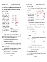
FIGURE 9-9: PORTE BLOCK DIAGRAM
IN I/O PORT MODE
Note: On a Power-on Reset, these pins are
configured as analog inputs.
CLRF PORTE ; Initialize PORTE by
; clearing output
; data latches
CLRF LATE ; Alternate method
; to clear output
; data latches
MOVLW 0x07 ; Configure A/D
MOVWF ADCON1 ; for digital inputs
MOVLW 0x05 ; Value used to
; initialize data
; direction
MOVWF TRISE ; Set RE<0> as inputs
; RE<1> as outputs
; RE<2> as inputs
Data
Bus
WR LATE
WR TRISE
RD PORTE
Data Latch
TRIS Latch
RD TRISE
Schmitt
Trigger
Input
Buffer
QD
CK
QD
CK
EN
QD
EN
I/O pin
(1)
RD LATE
or
PORTE
To Analog Converter
Note 1: I/O pins have diode protection to VDD and VSS.
PIC18FXX2
DS39564C-page 98 © 2006 Microchip Technology Inc.
REGISTER 9-1: TRISE REGISTER
R-0 R-0 R/W-0 R/W-0 U-0 R/W-1 R/W-1 R/W-1
IBF OBF IBOV PSPMODE
— TRISE2 TRISE1 TRISE0
bit 7 bit 0
bit 7 IBF: Input Buffer Full Status bit
1 = A word has been received and waiting to be read by the CPU
0 = No word has been received
bit 6 OBF: Output Buffer Full Status bit
1 = The output buffer still holds a previously written word
0 = The output buffer has been read
bit 5 IBOV: Input Buffer Overflow Detect bit (in Microprocessor mode)
1 = A write occurred when a previously input word has not been read
(must be cleared in software)
0 = No overflow occurred
bit 4 PSPMODE: Parallel Slave Port Mode Select bit
1 = Parallel Slave Port mode
0 = General purpose I/O mode
bit 3 Unimplemented: Read as '0'
bit 2 TRISE2: RE2 Direction Control bit
1 = Input
0 = Output
bit 1 TRISE1: RE1 Direction Control bit
1 = Input
0 = Output
bit 0 TRISE0: RE0 Direction Control bit
1 = Input
0 = Output
Legend:
R = Readable bit W = Writable bit U = Unimplemented bit, read as ‘0’
- n = Value at POR ’1’ = Bit is set ’0’ = Bit is cleared x = Bit is unknown
© 2006 Microchip Technology Inc. DS39564C-page 99
PIC18FXX2
TABLE 9-9: PORTE FUNCTIONS
TABLE 9-10: SUMMARY OF REGISTERS ASSOCIATED WITH PORTE
Name Bit# Buffer Type Function
RE0/RD
/AN5 bit0 ST/TTL
(1)
Input/output port pin or read control input in Parallel Slave Port mode
or analog input:
RD
1 = Not a read operation
0 = Read operation. Reads PORTD register (if chip selected).
RE1/WR/AN6 bit1 ST/TTL
(1)
Input/output port pin or write control input in Parallel Slave Port mode
or analog input:
WR
1 = Not a write operation
0 = Write operation. Writes PORTD register (if chip selected).
RE2/CS
/AN7 bit2 ST/TTL
(1)
Input/output port pin or chip select control input in Parallel Slave Port
mode or analog input:
CS
1 = Device is not selected
0 = Device is selected
Legend: ST = Schmitt Trigger input, TTL = TTL input
Note 1: Input buffers are Schmitt Triggers when in I/O mode and TTL buffers when in Parallel Slave Port mode.
Name Bit 7 Bit 6 Bit 5 Bit 4 Bit 3 Bit 2 Bit 1 Bit 0
Value on
POR, BOR
Value on
All Other
RESETS
PORTE
— — — — —RE2RE1RE0 -000 -000
LATE
— — — — — LATE Data Output Register -xxx -uuu
TRISE IBF OBF IBOV PSPMODE
— PORTE Data Direction bits 0000 -111 0000 -111
ADCON1
ADFM ADCS2 — — PCFG3 PCFG2 PCFG1 PCFG0 00 0000 00 0000
Legend: x = unknown, u = unchanged, - = unimplemented, read as '0'. Shaded cells are not used by PORTE.
PIC18FXX2
DS39564C-page 100 © 2006 Microchip Technology Inc.
9.6 Parallel Slave Port
The Parallel Slave Port is implemented on the 40-pin
devices only (PIC18F4X2).
PORTD operates as an 8-bit wide Parallel Slave Port,
or microprocessor port when control bit, PSPMODE
(TRISE<4>) is set. It is asynchronously readable and
writable by the external world through RD
control input
pin, RE0/RD
and WR control input pin, RE1/WR.
It can directly interface to an 8-bit microprocessor data
bus. The external microprocessor can read or write the
PORTD latch as an 8-bit latch. Setting bit PSPMODE
enables port pin RE0/RD
to be the RD input, RE1/WR
to be the WR input and RE2/CS to be the CS (chip
select) input. For this functionality, the corresponding
data direction bits of the TRISE register (TRISE<2:0>)
must be configured as inputs (set). The A/D port config-
uration bits PCFG2:PCFG0 (ADCON1<2:0>) must be
set, which will configure pins RE2:RE0 as digital I/O.
A write to the PSP occurs when both the CS
and WR
lines are first detected low. A read from the PSP occurs
when both the CS
and RD lines are first detected low.
The PORTE I/O pins become control inputs for the
microprocessor port when bit PSPMODE (TRISE<4>)
is set. In this mode, the user must make sure that the
TRISE<2:0> bits are set (pins are configured as digital
inputs), and the ADCON1 is configured for digital I/O.
In this mode, the input buffers are TTL.
FIGURE 9-10: PORTD AND PORTE
BLOCK DIAGRAM
(PARALLEL SLAVE
PORT)
FIGURE 9-11: PARALLEL SLAVE PORT WRITE WAVEFORMS
Data Bus
WR LATD
RDx
QD
CK
EN
QD
EN
RD PORTD
Pin
One bit of PORTD
Set Interrupt Flag
PSPIF (PIR1<7>)
Read
Chip Select
Write
RD
CS
WR
Note: I/O pin has protection diodes to VDD and VSS.
TTL
TTL
TTL
TTL
or
PORTD
RD LATD
Data Latch
TRIS Latch
Q1 Q2 Q3 Q4
CS
Q1 Q2 Q3 Q4 Q1 Q2 Q3 Q4
WR
RD
IBF
OBF
PSPIF
PORTD<7:0>
© 2006 Microchip Technology Inc. DS39564C-page 101
PIC18FXX2
FIGURE 9-12: PARALLEL SLAVE PORT READ WAVEFORMS
TABLE 9-11: REGISTERS ASSOCIATED WITH PARALLEL SLAVE PORT
Q1 Q2 Q3 Q4
CS
Q1 Q2 Q3 Q4 Q1 Q2 Q3 Q4
WR
IBF
PSPIF
RD
OBF
PORTD<7:0>
Name Bit 7 Bit 6 Bit 5 Bit 4 Bit 3 Bit 2 Bit 1 Bit 0
Value on
POR, BOR
Value on
All Other
RESETS
PORTD Port Data Latch when written; Port pins when read xxxx xxxx uuuu uuuu
LATD LATD Data Output bits xxxx xxxx uuuu uuuu
TRISD PORTD Data Direction bits 1111 1111 1111 1111
PORTE
— — — — —RE2RE1RE0 -000 -000
LATE
— — — — — LATE Data Output bits -xxx -uuu
TRISE IBF OBF IBOV PSPMODE
— PORTE Data Direction bits 0000 -111 0000 -111
INTCON GIE/
GIEH
PEIE/
GIEL
TMR0IF INT0IE RBIE TMR0IF INT0IF RBIF 0000 000x 0000 000u
PIR1 PSPIF
ADIF RCIF TXIF SSPIF CCP1IF TMR2IF TMR1IF 0000 0000 0000 0000
PIE1 PSPIE
ADIE RCIE TXIE SSPIE CCP1IE TMR2IE TMR1IE 0000 0000 0000 0000
IPR1 PSPIP
ADIP RCIP TXIP SSPIP CCP1IP TMR2IP TMR1IP 0000 0000 0000 0000
ADCON1
ADFM ADCS2 — — PCFG3 PCFG2 PCFG1 PCFG0 00 0000 00 0000
Legend: x = unknown, u = unchanged, - = unimplemented, read as '0'. Shaded cells are not used by the Parallel Slave Port.
PIC18FXX2
DS39564C-page 102 © 2006 Microchip Technology Inc.
NOTES:
© 2006 Microchip Technology Inc. DS39564C-page 103
PIC18FXX2
10.0 TIMER0 MODULE
The Timer0 module has the following features:
• Software selectable as an 8-bit or 16-bit timer/
counter
• Readable and writable
• Dedicated 8-bit software programmable prescaler
• Clock source selectable to be external or internal
• Interrupt-on-overflow from FFh to 00h in 8-bit
mode and FFFFh to 0000h in 16-bit mode
• Edge select for external clock
Figure 10-1 shows a simplified block diagram of the
Timer0 module in 8-bit mode and Figure 10-2 shows a
simplified block diagram of the Timer0 module in 16-bit
mode.
The T0CON register (Register 10-1) is a readable and
writable register that controls all the aspects of Timer0,
including the prescale selection.
REGISTER 10-1: T0CON: TIMER0 CONTROL REGISTER
R/W-1 R/W-1 R/W-1 R/W-1 R/W-1 R/W-1 R/W-1 R/W-1
TMR0ON T08BIT T0CS T0SE PSA T0PS2 T0PS1 T0PS0
bit 7 bit 0
bit 7 TMR0ON: Timer0 On/Off Control bit
1 = Enables Timer0
0 = Stops Timer0
bit 6 T08BIT: Timer0 8-bit/16-bit Control bit
1 = Timer0 is configured as an 8-bit timer/counter
0 = Timer0 is configured as a 16-bit timer/counter
bit 5 T0CS: Timer0 Clock Source Select bit
1 = Transition on T0CKI pin
0 = Internal instruction cycle clock (CLKO)
bit 4 T0SE: Timer0 Source Edge Select bit
1 = Increment on high-to-low transition on T0CKI pin
0 = Increment on low-to-high transition on T0CKI pin
bit 3 PSA: Timer0 Prescaler Assignment bit
1 = TImer0 prescaler is NOT assigned. Timer0 clock input bypasses prescaler.
0 = Timer0 prescaler is assigned. Timer0 clock input comes from prescaler output.
bit 2-0 T0PS2:T0PS0: Timer0 Prescaler Select bits
111 = 1:256 prescale value
110 = 1:128 prescale value
101 = 1:64 prescale value
100 = 1:32 prescale value
011 = 1:16 prescale value
010 = 1:8 prescale value
001 = 1:4 prescale value
000 = 1:2 prescale value
Legend:
R = Readable bit W = Writable bit U = Unimplemented bit, read as ‘0’
- n = Value at POR ’1’ = Bit is set ’0’ = Bit is cleared x = Bit is unknown
PIC18FXX2
DS39564C-page 104 © 2006 Microchip Technology Inc.
FIGURE 10-1: TIMER0 BLOCK DIAGRAM IN 8-BIT MODE
FIGURE 10-2: TIMER0 BLOCK DIAGRAM IN 16-BIT MODE
Note: Upon RESET, Timer0 is enabled in 8-bit mode with clock input from T0CKI max. prescale.
RA4/T0CKI pin
T0SE
0
1
1
0
T0CS
FOSC/4
Programmable
Prescaler
Sync with
Internal
Clocks
TMR0L
(2 TCY delay)
Data Bus
8
PSA
T0PS2, T0PS1, T0PS0
Set Interrupt
Flag bit TMR0IF
on Overflow
3
Note: Upon RESET, Timer0 is enabled in 8-bit mode with clock input from T0CKI max. prescale.
T0CKI pin
T0SE
0
1
1
0
T0CS
FOSC/4
Programmable
Prescaler
Sync with
Internal
Clocks
TMR0L
(2 TCY delay)
Data Bus<7:0>
8
PSA
T0PS2, T0PS1, T0PS0
Set Interrupt
Flag bit TMR0IF
on Overflow
3
TMR0
TMR0H
High Byte
8
8
8
Read TMR0L
Write TMR0L
© 2006 Microchip Technology Inc. DS39564C-page 105
PIC18FXX2
10.1 Timer0 Operation
Timer0 can operate as a timer or as a counter.
Timer mode is selected by clearing the T0CS bit. In
Timer mode, the Timer0 module will increment every
instruction cycle (without prescaler). If the TMR0L reg-
ister is written, the increment is inhibited for the follow-
ing two instruction cycles. The user can work around
this by writing an adjusted value to the TMR0L register.
Counter mode is selected by setting the T0CS bit. In
Counter mode, Timer0 will increment, either on every
rising or falling edge of pin RA4/T0CKI. The increment-
ing edge is determined by the Timer0 Source Edge
Select bit (T0SE). Clearing the T0SE bit selects the ris-
ing edge. Restrictions on the external clock input are
discussed below.
When an external clock input is used for Timer0, it must
meet certain requirements. The requirements ensure
the external clock can be synchronized with the internal
phase clock (T
OSC). Also, there is a delay in the actual
incrementing of Timer0 after synchronization.
10.2 Prescaler
An 8-bit counter is available as a prescaler for the Timer0
module. The prescaler is not readable or writable.
The PSA and T0PS2:T0PS0 bits determine the
prescaler assignment and prescale ratio.
Clearing bit PSA will assign the prescaler to the Timer0
module. When the prescaler is assigned to the Timer0
module, prescale values of 1:2, 1:4, , 1:256 are
selectable.
When assigned to the Timer0 module, all instructions
writing to the TMR0L register (e.g., CLRF TMR0,
MOVWF TMR0, BSF TMR0, x etc.) will clear the
prescaler count.
10.2.1 SWITCHING PRESCALER ASSIGNMENT
The prescaler assignment is fully under software con-
trol, (i.e., it can be changed “on-the-fly” during program
execution).
10.3 Timer0 Interrupt
The TMR0 interrupt is generated when the TMR0 reg-
ister overflows from FFh to 00h in 8-bit mode, or FFFFh
to 0000h in 16-bit mode. This overflow sets the TMR0IF
bit. The interrupt can be masked by clearing the
TMR0IE bit. The TMR0IE bit must be cleared in soft-
ware by the Timer0 module Interrupt Service Routine
before re-enabling this interrupt. The TMR0 interrupt
cannot awaken the processor from SLEEP, since the
timer is shut-off during SLEEP.
10.4 16-Bit Mode Timer Reads and
Writes
TMR0H is not the high byte of the timer/counter in
16-bit mode, but is actually a buffered version of the
high byte of Timer0 (refer to Figure 10-2). The high byte
of the Timer0 counter/timer is not directly readable nor
writable. TMR0H is updated with the contents of the
high byte of Timer0 during a read of TMR0L. This pro-
vides the ability to read all 16-bits of Timer0 without
having to verify that the read of the high and low byte
were valid due to a rollover between successive reads
of the high and low byte.
A write to the high byte of Timer0 must also take place
through the TMR0H buffer register. Timer0 high byte is
updated with the contents of TMR0H when a write
occurs to TMR0L. This allows all 16-bits of Timer0 to be
updated at once.
TABLE 10-1: REGISTERS ASSOCIATED WITH TIMER0
Note: Writing to TMR0L when the prescaler is
assigned to Timer0 will clear the prescaler
count, but will not change the prescaler
assignment.
Name Bit 7 Bit 6 Bit 5 Bit 4 Bit 3 Bit 2 Bit 1 Bit 0
Value on
POR, BOR
Value on
All Other
RESETS
TMR0L Timer0 Module Low Byte Register xxxx xxxx uuuu uuuu
TMR0H Timer0 Module High Byte Register 0000 0000 0000 0000
INTCON GIE/GIEH PEIE/GIEL TMR0IE
INT0IE RBIE TMR0IF INT0IF RBIF 0000 000x 0000 000u
T0CON TMR0ON T08BIT T0CS T0SE PSA T0PS2 T0PS1 T0PS0 1111 1111 1111 1111
TRISA
— PORTA Data Direction Register -111 1111 -111 1111
Legend: x = unknown, u = unchanged, - = unimplemented locations read as '0'. Shaded cells are not used by Timer0.
PIC18FXX2
DS39564C-page 106 © 2006 Microchip Technology Inc.
NOTES:
© 2006 Microchip Technology Inc. DS39564C-page 107
PIC18FXX2
11.0 TIMER1 MODULE
The Timer1 module timer/counter has the following
features:
• 16-bit timer/counter
(two 8-bit registers; TMR1H and TMR1L)
• Readable and writable (both registers)
• Internal or external clock select
• Interrupt-on-overflow from FFFFh to 0000h
• RESET from CCP module special event trigger
Figure 11-1 is a simplified block diagram of the Timer1
module.
Register 11-1 details the Timer1 control register. This
register controls the Operating mode of the Timer1
module, and contains the Timer1 oscillator enable bit
(T1OSCEN). Timer1 can be enabled or disabled by
setting or clearing control bit TMR1ON (T1CON<0>).
REGISTER 11-1: T1CON: TIMER1 CONTROL REGISTER
R/W-0 U-0 R/W-0 R/W-0 R/W-0 R/W-0 R/W-0 R/W-0
RD16
— T1CKPS1 T1CKPS0 T1OSCEN T1SYNC TMR1CS TMR1ON
bit 7 bit 0
bit 7 RD16: 16-bit Read/Write Mode Enable bit
1 = Enables register Read/Write of Timer1 in one 16-bit operation
0 = Enables register Read/Write of Timer1 in two 8-bit operations
bit 6 Unimplemented: Read as '0'
bit 5-4 T1CKPS1:T1CKPS0: Timer1 Input Clock Prescale Select bits
11 = 1:8 Prescale value
10 = 1:4 Prescale value
01 = 1:2 Prescale value
00 = 1:1 Prescale value
bit 3 T1OSCEN: Timer1 Oscillator Enable bit
1 = Timer1 Oscillator is enabled
0 = Timer1 Oscillator is shut-off
The oscillator inverter and feedback resistor are turned off to eliminate power drain.
bit 2 T1SYNC
: Timer1 External Clock Input Synchronization Select bit
When TMR1CS = 1:
1 = Do not synchronize external clock input
0 = Synchronize external clock input
When TMR1CS = 0:
This bit is ignored. Timer1 uses the internal clock when TMR1CS = 0.
bit 1 TMR1CS: Timer1 Clock Source Select bit
1 = External clock from pin RC0/T1OSO/T13CKI (on the rising edge)
0 = Internal clock (F
OSC/4)
bit 0 TMR1ON: Timer1 On bit
1 = Enables Timer1
0 = Stops Timer1
Legend:
R = Readable bit W = Writable bit U = Unimplemented bit, read as ‘0’
- n = Value at POR ’1’ = Bit is set ’0’ = Bit is cleared x = Bit is unknown
PIC18FXX2
DS39564C-page 108 © 2006 Microchip Technology Inc.
11.1 Timer1 Operation
Timer1 can operate in one of these modes:
•As a timer
• As a synchronous counter
• As an asynchronous counter
The Operating mode is determined by the clock select
bit, TMR1CS (T1CON<1>).
When TMR1CS = 0, Timer1 increments every instruc-
tion cycle. When TMR1CS = 1, Timer1 increments on
every rising edge of the external clock input or the
Timer1 oscillator, if enabled.
When the Timer1 oscillator is enabled (T1OSCEN is
set), the RC1/T1OSI and RC0/T1OSO/T1CKI pins
become inputs. That is, the TRISC<1:0> value is
ignored, and the pins are read as ‘0’.
Timer1 also has an internal “RESET input”. This
RESET can be generated by the CCP module
(Section 14.0).
FIGURE 11-1: TIMER1 BLOCK DIAGRAM
FIGURE 11-2: TIMER1 BLOCK DIAGRAM: 16-BIT READ/WRITE MODE
TMR1H
TMR1L
T1SYNC
TMR1CS
T1CKPS1:T1CKPS0
SLEEP Input
F
OSC/4
Internal
Clock
TMR1ON
On/Off
Prescaler
1, 2, 4, 8
Synchronize
det
1
0
0
1
Synchronized
Clock Input
2
TMR1IF
Overflow
TMR1
CLR
CCP Special Event Trigger
T1OSCEN
Enable
Oscillator
(1)
T1OSC
Interrupt
Flag Bit
Note 1: When enable bit T1OSCEN is cleared, the inverter and feedback resistor are turned off. This eliminates power drain.
T1OSI
T1CKI/T1OSO
Timer 1
TMR1L
T1OSC
T1SYNC
TMR1CS
T1CKPS1:T1CKPS0
SLEEP Input
T1OSCEN
Enable
Oscillator
(1)
TMR1IF
Overflow
Interrupt
F
OSC/4
Internal
Clock
TMR1ON
on/off
Prescaler
1, 2, 4, 8
Synchronize
det
1
0
0
1
Synchronized
Clock Input
2
T13CKI/T1OSO
T1OSI
TMR1
Flag bit
Note 1: When enable bit T1OSCEN is cleared, the inverter and feedback resistor are turned off. This eliminates power drain.
High Byte
Data Bus<7:0>
8
TMR1H
8
8
8
Read TMR1L
Write TMR1L
CLR
CCP Special Event Trigger
© 2006 Microchip Technology Inc. DS39564C-page 109
PIC18FXX2
11.2 Timer1 Oscillator
A crystal oscillator circuit is built-in between pins T1OSI
(input) and T1OSO (amplifier output). It is enabled by
setting control bit T1OSCEN (T1CON<3>). The oscilla-
tor is a low power oscillator rated up to 200 kHz. It will
continue to run during SLEEP. It is primarily intended
for a 32 kHz crystal. Table 11-1 shows the capacitor
selection for the Timer1 oscillator.
The user must provide a software time delay to ensure
proper start-up of the Timer1 oscillator.
TABLE 11-1: CAPACITOR SELECTION FOR
THE ALTERNATE
OSCILLATOR
11.3 Timer1 Interrupt
The TMR1 Register pair (TMR1H:TMR1L) increments
from 0000h to FFFFh and rolls over to 0000h. The
TMR1 Interrupt, if enabled, is generated on overflow,
which is latched in interrupt flag bit TMR1IF (PIR1<0>).
This interrupt can be enabled/disabled by setting/
clearing TMR1 interrupt enable bit, TMR1IE (PIE1<0>).
11.4 Resetting Timer1 using a CCP
Trigger Output
If the CCP module is configured in Compare mode to
generate a “special event trigger” (CCP1M3:CCP1M0
= 1011), this signal will reset Timer1 and start an A/D
conversion (if the A/D module is enabled).
Timer1 must be configured for either Timer or Synchro-
nized Counter mode to take advantage of this feature.
If Timer1 is running in Asynchronous Counter mode,
this RESET operation may not work.
In the event that a write to Timer1 coincides with a
special event trigger from CCP1, the write will take
precedence.
In this mode of operation, the CCPR1H:CCPR1L regis-
ters pair effectively becomes the period register for
Timer1.
11.5 Timer1 16-Bit Read/Write Mode
Timer1 can be configured for 16-bit reads and writes
(see Figure 11-2). When the RD16 control bit
(T1CON<7>) is set, the address for TMR1H is mapped
to a buffer register for the high byte of Timer1. A read
from TMR1L will load the contents of the high byte of
Timer1 into the Timer1 high byte buffer. This provides
the user with the ability to accurately read all 16-bits of
Timer1 without having to determine whether a read of
the high byte followed by a read of the low byte is valid,
due to a rollover between reads.
A write to the high byte of Timer1 must also take place
through the TMR1H buffer register. Timer1 high byte is
updated with the contents of TMR1H when a write
occurs to TMR1L. This allows a user to write all 16 bits
to both the high and low bytes of Timer1 at once.
The high byte of Timer1 is not directly readable or writ-
able in this mode. All reads and writes must take place
through the Timer1 high byte buffer register. Writes to
TMR1H do not clear the Timer1 prescaler. The
prescaler is only cleared on writes to TMR1L.
Osc Type Freq C1 C2
LP 32 kHz TBD
(1)
TBD
(1)
Crystal to be Tested:
32.768 kHz Epson C-001R32.768K-A ± 20 PPM
Note 1: Microchip suggests 33 pF as a starting
point in validating the oscillator circuit.
2: Higher capacitance increases the stability
of the oscillator, but also increases the
start-up time.
3: Since each resonator/crystal has its own
characteristics, the user should consult
the resonator/crystal manufacturer
for appropriate values of external
components.
4: Capacitor values are for design guidance
only.
Note: The special event triggers from the CCP1
module will not set interrupt flag bit
TMR1IF (PIR1<0>).
PIC18FXX2
DS39564C-page 110 © 2006 Microchip Technology Inc.
TABLE 11-2: REGISTERS ASSOCIATED WITH TIMER1 AS A TIMER/COUNTER
Name Bit 7 Bit 6 Bit 5 Bit 4 Bit 3 Bit 2 Bit 1 Bit 0
Value on
POR, BOR
Value on
All Other
RESETS
INTCON GIE/GIEH PEIE/GIEL
TMR0IE INT0IE RBIE TMR0IF INT0IF RBIF 0000 000x 0000 000u
PIR1
PSPIF
(1)
ADIF RCIF TXIF SSPIF CCP1IF TMR2IF TMR1IF 0000 0000 0000 0000
PIE1
PSPIE
(1)
ADIE RCIE TXIE SSPIE CCP1IE TMR2IE TMR1IE 0000 0000 0000 0000
IPR1
PSPIP
(1)
ADIP RCIP TXIP SSPIP CCP1IP TMR2IP TMR1IP 0000 0000 0000 0000
TMR1L Holding Register for the Least Significant Byte of the 16-bit TMR1 Register xxxx xxxx uuuu uuuu
TMR1H Holding Register for the Most Significant Byte of the 16-bit TMR1 Register xxxx xxxx uuuu uuuu
T1CON RD16
— T1CKPS1 T1CKPS0 T1OSCEN T1SYNC TMR1CS TMR1ON 0-00 0000 u-uu uuuu
Legend: x = unknown, u = unchanged, - = unimplemented, read as '0'. Shaded cells are not used by the Timer1 module.
Note 1: The PSPIF, PSPIE and PSPIP bits are reserved on the PIC18F2X2 devices; always maintain these bits clear.
© 2006 Microchip Technology Inc. DS39564C-page 111
PIC18FXX2
12.0 TIMER2 MODULE
The Timer2 module timer has the following features:
• 8-bit timer (TMR2 register)
• 8-bit period register (PR2)
• Readable and writable (both registers)
• Software programmable prescaler (1:1, 1:4, 1:16)
• Software programmable postscaler (1:1 to 1:16)
• Interrupt on TMR2 match of PR2
• SSP module optional use of TMR2 output to
generate clock shift
Timer2 has a control register shown in Register 12-1.
Timer2 can be shut-off by clearing control bit TMR2ON
(T2CON<2>) to minimize power consumption.
Figure 12-1 is a simplified block diagram of the Timer2
module. Register 12-1 shows the Timer2 control regis-
ter. The prescaler and postscaler selection of Timer2
are controlled by this register.
12.1 Timer2 Operation
Timer2 can be used as the PWM time-base for the
PWM mode of the CCP module. The TMR2 register is
readable and writable, and is cleared on any device
RESET. The input clock (F
OSC/4) has a prescale option
of 1:1, 1:4 or 1:16, selected by control bits
T2CKPS1:T2CKPS0 (T2CON<1:0>). The match out-
put of TMR2 goes through a 4-bit postscaler (which
gives a 1:1 to 1:16 scaling inclusive) to generate a
TMR2 interrupt (latched in flag bit TMR2IF, (PIR1<1>)).
The prescaler and postscaler counters are cleared
when any of the following occurs:
• a write to the TMR2 register
• a write to the T2CON register
• any device RESET (Power-on Reset, MCLR
Reset, Watchdog Timer Reset, or Brown-out
Reset)
TMR2 is not cleared when T2CON is written.
REGISTER 12-1: T2CON: TIMER2 CONTROL REGISTER
U-0 R/W-0 R/W-0 R/W-0 R/W-0 R/W-0 R/W-0 R/W-0
— TOUTPS3 TOUTPS2 TOUTPS1 TOUTPS0 TMR2ON T2CKPS1 T2CKPS0
bit 7 bit 0
bit 7 Unimplemented: Read as '0'
bit 6-3 TOUTPS3:TOUTPS0: Timer2 Output Postscale Select bits
0000 = 1:1 Postscale
0001 = 1:2 Postscale
•
•
•
1111 = 1:16 Postscale
bit 2 TMR2ON: Timer2 On bit
1 = Timer2 is on
0 = Timer2 is off
bit 1-0 T2CKPS1:T2CKPS0: Timer2 Clock Prescale Select bits
00 = Prescaler is 1
01 = Prescaler is 4
1x = Prescaler is 16
Legend:
R = Readable bit W = Writable bit U = Unimplemented bit, read as ‘0’
- n = Value at POR ’1’ = Bit is set ’0’ = Bit is cleared x = Bit is unknown
PIC18FXX2
DS39564C-page 112 © 2006 Microchip Technology Inc.
12.2 Timer2 Interrupt
The Timer2 module has an 8-bit period register, PR2.
Timer2 increments from 00h until it matches PR2 and
then resets to 00h on the next increment cycle. PR2 is
a readable and writable register. The PR2 register is
initialized to FFh upon RESET.
12.3 Output of TMR2
The output of TMR2 (before the postscaler) is fed to the
Synchronous Serial Port module, which optionally uses
it to generate the shift clock.
FIGURE 12-1: TIMER2 BLOCK DIAGRAM
TABLE 12-1: REGISTERS ASSOCIATED WITH TIMER2 AS A TIMER/COUNTER
Comparator
TMR2
Sets Flag
TMR2
Output
(1)
RESET
Postscaler
Prescaler
PR2
2
F
OSC/4
1:1 to 1:16
1:1, 1:4, 1:16
EQ
4
bit TMR2IF
Note 1: TMR2 register output can be software selected by the SSP Module as a baud clock.
TOUTPS3:TOUTPS0
T2CKPS1:T2CKPS0
Name Bit 7 Bit 6 Bit 5 Bit 4 Bit 3 Bit 2 Bit 1 Bit 0
Value on
POR, BOR
Value on
All Other
RESETS
INTCON GIE/GIEH PEIE/GIEL
TMR0IE INT0IE RBIE TMR0IF INT0IF RBIF 0000 000x 0000 000u
PIR1
PSPIF
(1)
ADIF RCIF TXIF SSPIF CCP1IF TMR2IF TMR1IF 0000 0000 0000 0000
PIE1
PSPIE
(1)
ADIE RCIE TXIE SSPIE CCP1IE TMR2IE TMR1IE 0000 0000 0000 0000
IPR1
PSPIP
(1)
ADIP RCIP TXIP SSPIP CCP1IP TMR2IP TMR1IP 0000 0000 0000 0000
TMR2 Timer2 Module Register 0000 0000 0000 0000
T2CON
— TOUTPS3 TOUTPS2 TOUTPS1 TOUTPS0 TMR2ON T2CKPS1 T2CKPS0 -000 0000 -000 0000
PR2 Timer2 Period Register 1111 1111 1111 1111
Legend: x = unknown, u = unchanged, - = unimplemented read as '0'. Shaded cells are not used by the Timer2 module.
Note 1: The PSPIF, PSPIE and PSPIP bits are reserved on the PIC18F2X2 devices; always maintain these bits clear.
© 2006 Microchip Technology Inc. DS39564C-page 113
PIC18FXX2
13.0 TIMER3 MODULE
The Timer3 module timer/counter has the following
features:
• 16-bit timer/counter
(two 8-bit registers; TMR3H and TMR3L)
• Readable and writable (both registers)
• Internal or external clock select
• Interrupt-on-overflow from FFFFh to 0000h
• RESET from CCP module trigger
Figure 13-1 is a simplified block diagram of the Timer3
module.
Register 13-1 shows the Timer3 control register. This
register controls the Operating mode of the Timer3
module and sets the CCP clock source.
Register 11-1 shows the Timer1 control register. This
register controls the Operating mode of the Timer1
module, as well as contains the Timer1 oscillator
enable bit (T1OSCEN), which can be a clock source for
Timer3.
REGISTER 13-1: T3CON: TIMER3 CONTROL REGISTER
R/W-0 R/W-0 R/W-0 R/W-0 R/W-0 R/W-0 R/W-0 R/W-0
RD16 T3CCP2 T3CKPS1 T3CKPS0 T3CCP1 T3SYNC TMR3CS TMR3ON
bit 7 bit 0
bit 7 RD16: 16-bit Read/Write Mode Enable bit
1 = Enables register Read/Write of Timer3 in one 16-bit operation
0 = Enables register Read/Write of Timer3 in two 8-bit operations
bit 6-3 T3CCP2:T3CCP1: Timer3 and Timer1 to CCPx Enable bits
1x = Timer3 is the clock source for compare/capture CCP modules
01 = Timer3 is the clock source for compare/capture of CCP2,
Timer1 is the clock source for compare/capture of CCP1
00 = Timer1 is the clock source for compare/capture CCP modules
bit 5-4 T3CKPS1:T3CKPS0: Timer3 Input Clock Prescale Select bits
11 = 1:8 Prescale value
10 = 1:4 Prescale value
01 = 1:2 Prescale value
00 = 1:1 Prescale value
bit 2 T3SYNC
: Timer3 External Clock Input Synchronization Control bit
(Not usable if the system clock comes from Timer1/Timer3)
When TMR3CS = 1:
1 = Do not synchronize external clock input
0 = Synchronize external clock input
When TMR3CS = 0:
This bit is ignored. Timer3 uses the internal clock when TMR3CS = 0.
bit 1 TMR3CS: Timer3 Clock Source Select bit
1 = External clock input from Timer1 oscillator or T1CKI
(on the rising edge after the first falling edge)
0 = Internal clock (F
OSC/4)
bit 0 TMR3ON: Timer3 On bit
1 = Enables Timer3
0 = Stops Timer3
Legend:
R = Readable bit W = Writable bit U = Unimplemented bit, read as ‘0’
- n = Value at POR ’1’ = Bit is set ’0’ = Bit is cleared x = Bit is unknown
PIC18FXX2
DS39564C-page 114 © 2006 Microchip Technology Inc.
13.1 Timer3 Operation
Timer3 can operate in one of these modes:
•As a timer
• As a synchronous counter
• As an asynchronous counter
The Operating mode is determined by the clock select
bit, TMR3CS (T3CON<1>).
When TMR3CS = 0, Timer3 increments every instruc-
tion cycle. When TMR3CS = 1, Timer3 increments on
every rising edge of the Timer1 external clock input or
the Timer1 oscillator, if enabled.
When the Timer1 oscillator is enabled (T1OSCEN is
set), the RC1/T1OSI and RC0/T1OSO/T1CKI pins
become inputs. That is, the TRISC<1:0> value is
ignored, and the pins are read as ‘0’.
Timer3 also has an internal “RESET input”. This RESET
can be generated by the CCP module (Section 14.0).
FIGURE 13-1: TIMER3 BLOCK DIAGRAM
FIGURE 13-2: TIMER3 BLOCK DIAGRAM CONFIGURED IN 16-BIT READ/WRITE MODE
TMR3H TMR3L
T1OSC
T3SYNC
TMR3CS
T3CKPS1:T3CKPS0
SLEEP Input
T1OSCEN
Enable
Oscillator
(1)
TMR3IF
Overflow
Interrupt
F
OSC/4
Internal
Clock
TMR3ON
On/Off
Prescaler
1, 2, 4, 8
Synchronize
det
1
0
0
1
Synchronized
Clock Input
2
T1OSO/
T1OSI
Flag bit
(3)
Note 1: When enable bit T1OSCEN is cleared, the inverter and feedback resistor are turned off. This eliminates power drain.
T13CKI
CLR
CCP Special Trigger
T3CCPx
Timer3
TMR3L
T1OSC
T3SYNC
TMR3CS
T3CKPS1:T3CKPS0
SLEEP Input
T1OSCEN
Enable
Oscillator
(1)
FOSC/4
Internal
Clock
TMR3ON
On/Off
Prescaler
1, 2, 4, 8
Synchronize
det
1
0
0
1
Synchronized
Clock Input
2
T1OSO/
T1OSI
TMR3
T13CKI
CLR
CCP Special Trigger
T3CCPx
To Timer1 Clock Input
Note 1: When the T1OSCEN bit is cleared, the inverter and feedback resistor are turned off. This eliminates power drain.
High Byte
Data Bus<7:0>
8
TMR3H
8
8
8
Read TMR3L
Write TMR3L
Set TMR3IF Flag bit
on Overflow
© 2006 Microchip Technology Inc. DS39564C-page 115
PIC18FXX2
13.2 Timer1 Oscillator
The Timer1 oscillator may be used as the clock source
for Timer3. The Timer1 oscillator is enabled by setting
the T1OSCEN (T1CON<3>) bit. The oscillator is a low
power oscillator rated up to 200 KHz. See Section 11.0
for further details.
13.3 Timer3 Interrupt
The TMR3 Register pair (TMR3H:TMR3L) increments
from 0000h to FFFFh and rolls over to 0000h. The
TMR3 Interrupt, if enabled, is generated on overflow,
which is latched in interrupt flag bit, TMR3IF
(PIR2<1>). This interrupt can be enabled/disabled by
setting/clearing TMR3 interrupt enable bit, TMR3IE
(PIE2<1>).
13.4 Resetting Timer3 Using a CCP
Trigger Output
If the CCP module is configured in Compare mode to
generate a “special event trigger” (CCP1M3:CCP1M0
= 1011), this signal will reset Timer3.
Timer3 must be configured for either Timer or Synchro-
nized Counter mode to take advantage of this feature.
If Timer3 is running in Asynchronous Counter mode,
this RESET operation may not work. In the event that a
write to Timer3 coincides with a special event trigger
from CCP1, the write will take precedence. In this mode
of operation, the CCPR1H:CCPR1L registers pair
effectively becomes the period register for Timer3.
TABLE 13-1: REGISTERS ASSOCIATED WITH TIMER3 AS A TIMER/COUNTER
Note: The special event triggers from the CCP
module will not set interrupt flag bit,
TMR3IF (PIR1<0>).
Name Bit 7 Bit 6 Bit 5 Bit 4 Bit 3 Bit 2 Bit 1 Bit 0
Value on
POR, BOR
Value on
All Other
RESETS
INTCON GIE/
GIEH
PEIE/
GIEL
TMR0IE INT0IE RBIE TMR0IF INT0IF RBIF 0000 000x 0000 000u
PIR2
— — — EEIF BCLIF LVDIF TMR3IF CCP2IF 0 0000 0 0000
PIE2
— — — EEIE BCLIE LVDIE TMR3IE CCP2IE 0 0000 0 0000
IPR2
— — — EEIP BCLIP LVDIP TMR3IP CCP2IP 1 1111 1 1111
TMR3L Holding Register for the Least Significant Byte of the 16-bit TMR3 Register xxxx xxxx uuuu uuuu
TMR3H Holding Register for the Most Significant Byte of the 16-bit TMR3 Register xxxx xxxx uuuu uuuu
T1CON RD16
— T1CKPS1 T1CKPS0 T1OSCEN T1SYNC TMR1CS TMR1ON 0-00 0000 u-uu uuuu
T3CON
RD16 T3CCP2 T3CKPS1 T3CKPS0 T3CCP1 T3SYNC TMR3CS TMR3ON 0000 0000 uuuu uuuu
Legend: x = unknown, u = unchanged, - = unimplemented, read as '0'. Shaded cells are not used by the Timer1 module.
PIC18FXX2
DS39564C-page 116 © 2006 Microchip Technology Inc.
NOTES:
© 2006 Microchip Technology Inc. DS39564C-page 117
PIC18FXX2
14.0 CAPTURE/COMPARE/PWM
(CCP) MODULES
Each CCP (Capture/Compare/PWM) module contains
a 16-bit register which can operate as a 16-bit Capture
register, as a 16-bit Compare register or as a PWM
Master/Slave Duty Cycle register. Table 14-1 shows
the timer resources of the CCP Module modes.
The operation of CCP1 is identical to that of CCP2, with
the exception of the special event trigger. Therefore,
operation of a CCP module in the following sections is
described with respect to CCP1.
Table 14-2 shows the interaction of the CCP modules.
REGISTER 14-1: CCP1CON REGISTER/CCP2CON REGISTER
U-0 U-0 R/W-0 R/W-0 R/W-0 R/W-0 R/W-0 R/W-0
— — DCxB1 DCxB0 CCPxM3 CCPxM2 CCPxM1 CCPxM0
bit 7 bit 0
bit 7-6 Unimplemented: Read as '0'
bit 5-4 DCxB1:DCxB0: PWM Duty Cycle bit1 and bit0
Capture mode:
Unused
Compare mode:
Unused
PWM mode:
These bits are the two LSbs (bit1 and bit0) of the 10-bit PWM duty cycle. The upper eight bits
(DCx9:DCx2) of the duty cycle are found in CCPRxL.
bit 3-0 CCPxM3:CCPxM0: CCPx Mode Select bits
0000 = Capture/Compare/PWM disabled (resets CCPx module)
0001 = Reserved
0010 = Compare mode, toggle output on match (CCPxIF bit is set)
0011 = Reserved
0100 = Capture mode, every falling edge
0101 = Capture mode, every rising edge
0110 = Capture mode, every 4th rising edge
0111 = Capture mode, every 16th rising edge
1000 = Compare mode,
Initialize CCP pin Low, on compare match force CCP pin High (CCPIF bit is set)
1001 = Compare mode,
Initialize CCP pin High, on compare match force CCP pin Low (CCPIF bit is set)
1010 = Compare mode,
Generate software interrupt on compare match (CCPIF bit is set, CCP pin is unaffected)
1011 = Compare mode,
Trigger special event (CCPIF bit is set)
11xx =PWM mode
Legend:
R = Readable bit W = Writable bit U = Unimplemented bit, read as ‘0’
- n = Value at POR ’1’ = Bit is set ’0’ = Bit is cleared x = Bit is unknown
PIC18FXX2
DS39564C-page 118 © 2006 Microchip Technology Inc.
14.1 CCP1 Module
Capture/Compare/PWM Register 1 (CCPR1) is com-
prised of two 8-bit registers: CCPR1L (low byte) and
CCPR1H (high byte). The CCP1CON register controls
the operation of CCP1. All are readable and writable.
TABLE 14-1: CCP MODE - TIMER
RESOURCE
14.2 CCP2 Module
Capture/Compare/PWM Register2 (CCPR2) is com-
prised of two 8-bit registers: CCPR2L (low byte) and
CCPR2H (high byte). The CCP2CON register controls
the operation of CCP2. All are readable and writable.
TABLE 14-2: INTERACTION OF TWO CCP MODULES
CCP Mode Timer Resource
Capture
Compare
PWM
Timer1 or Timer3
Timer1 or Timer3
Timer2
CCPx Mode CCPy Mode Interaction
Capture Capture TMR1 or TMR3 time-base. Time-base can be different for each CCP.
Capture Compare The compare could be configured for the special event trigger,
which clears either TMR1 or TMR3 depending upon which time-base is used.
Compare Compare The compare(s) could be configured for the special event trigger,
which clears TMR1 or TMR3 depending upon which time-base is used.
PWM PWM The PWMs will have the same frequency and update rate
(TMR2 interrupt).
PWM Capture None
PWM Compare None
© 2006 Microchip Technology Inc. DS39564C-page 119
PIC18FXX2
14.3 Capture Mode
In Capture mode, CCPR1H:CCPR1L captures the
16-bit value of the TMR1 or TMR3 registers when an
event occurs on pin RC2/CCP1. An event is defined as
one of the following:
• every falling edge
• every rising edge
• every 4th rising edge
• every 16th rising edge
The event is selected by control bits CCP1M3:CCP1M0
(CCP1CON<3:0>). When a capture is made, the inter-
rupt request flag bit CCP1IF (PIR1<2>) is set; it must be
cleared in software. If another capture occurs before the
value in register CCPR1 is read, the old captured value
is overwritten by the new captured value.
14.3.1 CCP PIN CONFIGURATION
In Capture mode, the RC2/CCP1 pin should be
configured as an input by setting the TRISC<2> bit.
14.3.2 TIMER1/TIMER3 MODE SELECTION
The timers that are to be used with the capture feature
(either Timer1 and/or Timer3) must be running in Timer
mode or Synchronized Counter mode. In Asynchro-
nous Counter mode, the capture operation may not
work. The timer to be used with each CCP module is
selected in the T3CON register.
14.3.3 SOFTWARE INTERRUPT
When the Capture mode is changed, a false capture
interrupt may be generated. The user should keep bit
CCP1IE (PIE1<2>) clear to avoid false interrupts and
should clear the flag bit, CCP1IF, following any such
change in Operating mode.
14.3.4 CCP PRESCALER
There are four prescaler settings, specified by bits
CCP1M3:CCP1M0. Whenever the CCP module is
turned off or the CCP module is not in Capture mode,
the prescaler counter is cleared. This means that any
RESET will clear the prescaler counter.
Switching from one capture prescaler to another may
generate an interrupt. Also, the prescaler counter will
not be cleared, therefore, the first capture may be from
a non-zero prescaler. Example 14-1 shows the recom-
mended method for switching between capture pres-
calers. This example also clears the prescaler counter
and will not generate the “false” interrupt.
EXAMPLE 14-1: CHANGING BETWEEN
CAPTURE PRESCALERS
FIGURE 14-1: CAPTURE MODE OPERATION BLOCK DIAGRAM
Note: If the RC2/CCP1 is configured as an out-
put, a write to the port can cause a capture
condition.
CLRF CCP1CON, F ; Turn CCP module off
MOVLW NEW_CAPT_PS ; Load WREG with the
; new prescaler mode
; value and CCP ON
MOVWF CCP1CON ; Load CCP1CON with
; this value
CCPR1H CCPR1L
TMR1H TMR1L
Set Flag bit CCP1IF
TMR3
Enable
Q’s
CCP1CON<3:0>
CCP1 pin
Prescaler
÷ 1, 4, 16
and
Edge Detect
TMR3H TMR3L
TMR1
Enable
T3CCP2
T3CCP2
CCPR2H CCPR2L
TMR1H TMR1L
Set Flag bit CCP2IF
TMR3
Enable
Q’s
CCP2CON<3:0>
CCP2 pin
Prescaler
÷ 1, 4, 16
and
Edge Detect
TMR3H TMR3L
TMR1
Enable
T3CCP2
T3CCP1
T3CCP2
T3CCP1
PIC18FXX2
DS39564C-page 120 © 2006 Microchip Technology Inc.
14.4 Compare Mode
In Compare mode, the 16-bit CCPR1 (CCPR2) register
value is constantly compared against either the TMR1
register pair value, or the TMR3 register pair value.
When a match occurs, the RC2/CCP1 (RC1/CCP2) pin
is:
• driven High
• driven Low
• toggle output (High to Low or Low to High)
• remains unchanged
The action on the pin is based on the value of control
bits CCP1M3:CCP1M0 (CCP2M3:CCP2M0). At the
same time, interrupt flag bit CCP1IF (CCP2IF) is set.
14.4.1 CCP PIN CONFIGURATION
The user must configure the CCPx pin as an output by
clearing the appropriate TRISC bit.
14.4.2 TIMER1/TIMER3 MODE SELECTION
Timer1 and/or Timer3 must be running in Timer mode
or Synchronized Counter mode if the CCP module is
using the compare feature. In Asynchronous Counter
mode, the compare operation may not work.
14.4.3 SOFTWARE INTERRUPT MODE
When generate software interrupt is chosen, the CCP1
pin is not affected. Only a CCP interrupt is generated (if
enabled).
14.4.4 SPECIAL EVENT TRIGGER
In this mode, an internal hardware trigger is generated,
which may be used to initiate an action.
The special event trigger output of CCP1 resets the
TMR1 register pair. This allows the CCPR1 register to
effectively be a 16-bit programmable period register for
Timer1.
The special trigger output of CCPx resets either the
TMR1 or TMR3 register pair. Additionally, the CCP2
Special Event Trigger will start an A/D conversion if the
A/D module is enabled.
FIGURE 14-2: COMPARE MODE OPERATION BLOCK DIAGRAM
Note: Clearing the CCP1CON register will force
the RC2/CCP1 compare output latch to the
default low level. This is not the PORTC
I/O data latch.
Note: The special event trigger from the CCP2
module will not set the Timer1 or Timer3
interrupt flag bits.
CCPR1H CCPR1L
TMR1H TMR1L
Comparator
QS
R
Output
Logic
Special Event Trigger
Set Flag bit CCP1IF
Match
RC2/CCP1 pin
TRISC<2>
CCP1CON<3:0>
Mode Select
Output Enable
Special Event Trigger will:
Reset Timer1 or Timer3, but not set Timer1 or Timer3 interrupt flag bit,
and set bit GO/DONE (ADCON0<2>)
which starts an A/D conversion (CCP2 only)
TMR3H TMR3L
T3CCP2
CCPR2H CCPR2L
Comparator
1
0
T3CCP2
T3CCP1
QS
R
Output
Logic
Special Event Trigger
Set Flag bit CCP2IF
Match
RC1/CCP2 pin
TRISC<1>
CCP2CON<3:0>
Mode Select
Output Enable
01
© 2006 Microchip Technology Inc. DS39564C-page 121
PIC18FXX2
TABLE 14-3: REGISTERS ASSOCIATED WITH CAPTURE, COMPARE, TIMER1 AND TIMER3
Name Bit 7 Bit 6 Bit 5 Bit 4 Bit 3 Bit 2 Bit 1 Bit 0
Value on
POR, BOR
Value on
All Other
RESETS
INTCON GIE/GIEH PEIE/GIEL
TMR0IE INT0IE RBIE TMR0IF INT0IF RBIF 0000 000x 0000 000u
PIR1
PSPIF
(1)
ADIF RCIF TXIF SSPIF CCP1IF TMR2IF TMR1IF 0000 0000 0000 0000
PIE1
PSPIE
(1)
ADIE RCIE TXIE SSPIE CCP1IE TMR2IE TMR1IE 0000 0000 0000 0000
IPR1
PSPIP
(1)
ADIP RCIP TXIP SSPIP CCP1IP TMR2IP TMR1IP 0000 0000 0000 0000
TRISC PORTC Data Direction Register 1111 1111 1111 1111
TMR1L Holding Register for the Least Significant Byte of the 16-bit TMR1 Register xxxx xxxx uuuu uuuu
TMR1H Holding Register for the Most Significant Byte of the 16-bit TMR1 Register xxxx xxxx uuuu uuuu
T1CON RD16
— T1CKPS1 T1CKPS0 T1OSCEN T1SYNC TMR1CS TMR1ON 0-00 0000 u-uu uuuu
CCPR1L Capture/Compare/PWM Register1 (LSB) xxxx xxxx uuuu uuuu
CCPR1H Capture/Compare/PWM Register1 (MSB) xxxx xxxx uuuu uuuu
CCP1CON
— — DC1B1 DC1B0 CCP1M3 CCP1M2 CCP1M1 CCP1M0 00 0000 00 0000
CCPR2L Capture/Compare/PWM Register2 (LSB) xxxx xxxx uuuu uuuu
CCPR2H Capture/Compare/PWM Register2 (MSB) xxxx xxxx uuuu uuuu
CCP2CON
— — DC2B1 DC2B0 CCP2M3 CCP2M2 CCP2M1 CCP2M0 00 0000 00 0000
PIR2
— — — EEIE BCLIF LVDIF TMR3IF CCP2IF 0 0000 0 0000
PIE2
— — — EEIF BCLIE LVDIE TMR3IE CCP2IE 0 0000 0 0000
IPR2
— — — EEIP BCLIP LVDIP TMR3IP CCP2IP 1 1111 1 1111
TMR3L Holding Register for the Least Significant Byte of the 16-bit TMR3 Register xxxx xxxx uuuu uuuu
TMR3H Holding Register for the Most Significant Byte of the 16-bit TMR3 Register xxxx xxxx uuuu uuuu
T3CON RD16 T3CCP2 T3CKPS1 T3CKPS0 T3CCP1 T3SYNC
TMR3CS TMR3ON 0000 0000 uuuu uuuu
Legend: x = unknown, u = unchanged, - = unimplemented, read as '0'. Shaded cells are not used by Capture and Timer1.
Note 1: The PSPIF, PSPIE and PSPIP bits are reserved on the PIC18F2x2 devices; always maintain these bits clear.