Smart Material Systems and MEMS - Vijay K. Varadan Part 3 pot
Bạn đang xem bản rút gọn của tài liệu. Xem và tải ngay bản đầy đủ của tài liệu tại đây (865.54 KB, 30 trang )
First, we will discuss an accelerometer consisting of
a proof mass suspended over an FET, with the gate
electrode of the device attached to the suspended
structure. The anchors of the ‘meander’ support are
elevated to suspend the beam above the gate region
(Figure 3.12). This arrangement provides a gap
between the gate and the insulator layer, thus keeping
the threshold voltage for the FET constant [16]. The
meander beams attached to this system are configured
such that the electrode moves in the direction shown in
Figure 3.12.
This motion of the gate electrode changes the transis-
tor drain current without affecting the current density
through the channel. The sensitivity S of this device is
given by the following:
S ¼
dI
D
dW
ðA=mÞð3:18Þ
where dI
D
is the change in drain current and dW is the
change in the depth to which the gate is overlapping the
channel.
Vacuum
cover
enclosur
Drive
line
(a)
(b)
(c)
(d)
Contacts for
sense lines
Resonant
microbeam
Silicon
diaphragm
Silicon Proof mass
Silicon flexure
P
1
P
2
V
in
V
a
V
+
V
–
V
T
Beam
To p
Substrate
I
DC
Sense resistor
Detector
AGC amplifier
Counter out
V
out
Beam
drive
Voltage-controlled
attenuator
Differental
amplifier
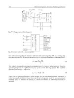
Figure 3.11 Resonant microbeam system (a) showing cross-sectional views of the polysilicon beam attached to a silicon diaphragm
(b) or silicon flexure (c), along with (d) a schematic of the related microbeam test circuit [15]. Reprinted from Sensors Actuators A,
35, Zook J D, Burns D W, Guckel H, Sniegowski J J, Engelstad R L and Feng Z, Characteristics of polysilicon resonant microbeams,
pp. 51–59, Copyright 1992, with permission from Elsevier
54 Smart Material Systems and MEMS
For a typical n-channel FET, the drain current is given
by:
I
D
¼
C
g
mW
2L
½2ðV
GS
ÀV
T
ÞV
DS
ÀV
2
DS
for V
DS
<V
GS
ÀV
T
ð3:19Þ
and:
I
D
¼
C
g
mW
2L
ðV
GS
À V
T
Þ
2
for V
DS
! V
GS
À V
T
ð3:20Þ
where V
GS
and V
DS
are the gate-to-source and drain-to-
source voltages, V
T
is the threshold voltage at which the
channel begins to conduct, C
g
is the gate capacitance per
unit gate area, m is the majority carrier mobility for the
channel and W and L are the width and length of the
channel, respectively. These equations show a linear
relationship between the drain current and the channel
width W.
The threshold voltage for the FET is as follows:
V
T
¼ V
FB
À
Q
D
C
i
À
ffiffiffiffiffiffiffiffiffiffiffiffiffiffiffiffiffiffiffiffiffiffiffiffiffiffiffiffiffiffiffiffiffiffiffiffi
2qeN
D
ðV
bi
À V
BS
Þ
p
C
i
ð3:21Þ
where Q
D
is the dose of the n-type impurity, N
D
is
the doping concentration, e is the dielectric constant of
the semiconductor and V
FB
, V
bi
and V
BS
are the flat-band
voltage, built-in potential of the channel junction and
substrate bias, respectively; C
i
is the capacitance of
the gate, which is a series combination of the capacitance
due to the air gap and that due to the insulator layer.
For very thin insulator layers, this capacitance can be
approximated to that due to air alone. Thus, the config-
uration presented here results in a linear relationship
for the device current to the mechanical motion. Further-
more, the lateral motion permits larger amplitudes of
variation. The inertial force of the mass causes the
lateral movement when the device can be used as an
accelerometer.
Substrate
Structural layer
Gate electrode
Insulator
Channel
Source
Drain
(b)
(a)
Meander beam
Insulator
Drain
Source
Anchor
Direction o
f
vibration
Polymer
Structural layer
Gate electrode
Channel
Source
Drain
Gate
L
W
Gate/anchor
Figure 3.12 Schematics of a movable-gate field effect transistor: (a) top view; (b) cross-sectional view.
Sensors for Smart Systems 55
Table 3.1 Structures of Love, SAW, SH–SAW, SH–APM and FPW devices and comparison of their operation [17,18]. M. Hoummady,
A. Campitelli and W. Wlodarski, ‘‘Acoustic wave sensors: design, sensing mechanisms and applications,’’ Smart Mater. Struct. 6 1997, # IOP
Device type Substrate Typical Structure Particle displacement Transverse component Sensing
frequency relative to wave relative to sensing medium/
propagation surface quantity
Love ST-quartz 95–130 MHz
Transverse Parallel Ice, liquid
Rayleigh SAW ST-quartz 80 MHz–1 GHz
Transverse parallel Normal Strain, gas
SH–SAW LiTaO
3
90–150 MHz Transverse Parallel Gas, liquid
SH–APM ST-quartz 160 MHz
Transverse Parallel Gas, liquid,
chemical
Lamb/FPW Si
x
N
y
=ZnO 1–6 MHz Transverse parallel Normal Gas, liquid
3.10 ACOUSTIC SENSORS
Acoustic sensors operate by converting electrical energy
in to acoustic waves, the propagation characteristics of
which could be influenced by the physical parameter
being measured, and then converting this back to
electrical energy for further processing. Various config-
urations of acoustic wave devices are possible for sensor
applications. The important characteristics of some of
these devices are summarized in Table 3.1. The type of
acoustic wave generated in a piezoelectric material
depends mainly on the substrate material properties, the
crystal cut and the structure of the electrodes utilized to
transform the electrical energy into mechanical energy.
A Rayleigh wave has both a surface-normal compo-
nent and a surface-parallel component in the direction of
propagation. The wave velocity is determined by the
substrate material and the crystal cut. Most surface
acoustic wave (SAW) devices operate under this mode
and will be discussed further below. The energies of the
SAW are confined to a zone close to the surface a few
wavelengths thick [19]. Love waves are guided acoustic
modes which propagate in a thin layer deposited on a
substrate. The acoustic energy is concentrated in this
guiding layer and results in a high-mass sensitivity. This
wave mode is typically employed in gases, biochemical
or viscosity sensors.
The selection of a different crystal cut can yield shear
horizontal (SH) surface waves instead of Rayleigh
waves. The particle displacements of this wave are
transverse to the wave propagation direction and parallel
to the plane of the surface. The frequency of operation is
determined by the inter-digitated transducer (IDT) finger
spacing and the shear horizontal wave velocity for the
particular substrate material. These have shown consid-
erable promise in applications such as sensors in liquid
media and biosensors [20–22]. In general, SH–SAWs are
sensitive to mass loading, viscosity, conductivity and
permittivity of the adjacent liquid.
The configuration of SH–APM devices is similar to
the Rayleigh SAW devices, but the wafer is thinner,
typically a few acoustic wavelengths. SH waves excited
by the transducer propagate in the bulk of the substrate,
at an angle to the surface. These waves reflect between
the plate surfaces as they travel in the plate between
the input and output transducers. The frequency of
operation is determined by the thickness of the plate
and the design of the transducer. SH–APM devices are
mainly used in liquid sensing and offer the advantage of
using the back surface of the plate as the sensing active
area.
Lamb waves, also known as flexural plate waves
(FPWs), are elastic waves that propagate in plates of
finite thickness and are used for the health monitoring
of structures and for flow sensors: as the fluid passes
through a channel above the acoustic path, it affects the
properties of the acoustic waves propagating on the
substrate.
Surface acoustic wave (SAW)-based sensors form
an important part of the sensor family and in recent
years have seen diverse applications ranging from gas
and vapor detection to strain measurement [19]. SAW
devices were first used in radar and communication
equipment as filters and delay lines and were recently
found to have several applications in sensors for various
physical variables, including temperature, pressure,
force, electric field and magnetic field, as well as che-
mical compounds. A SAW device consists of a piezo-
electric wafer, IDTs and reflectors on its surface. The
IDT is the ‘cornerstone’ of SAW technology, converting
the electrical energy into mechanical energy, and vice
versa, and hence are used for exciting as well as detecting
the SAW.
An IDT consists of two metal comb-shaped electrodes
placed on a piezoelectric substrate (Figure 3.13). An
electric field, created by the voltage applied to the
electrodes, induces dynamic strains in the piezoelectric
substrate, which in turn launches elastic waves.
These waves contain, among others, the Rayleigh
waves which run perpendicular to the electrodes with
velocity V
R
.
If a harmonic voltage, v ¼ v
0
exp ( jot), is applied to
the electrodes, the stress induced by a finger pair travels
along the surface of the crystal in both directions. To
ensure constructive interference and in-phase stress, the
distance between two neighboring fingers should be
equal to half the elastic wavelength, l
R
.
d ¼ l
R
=2 ð3:22Þ
v
d
Figure 3.13 Finger spacings and (d) and their role in determi-
nation of the acoustic wavelength (n) in an inter-digitated
transducer [23].
Sensors for Smart Systems 57
The associated frequency is known as the synchronous
frequency and is given by the following:
f
0
¼ V
R
=l
R
ð3:23Þ
At this frequency, the transducer efficiency in converting
electrical energy to acoustical, or vice versa, is max-
imized. The width of each electrode finger is generally
chosen as half the period. Its length determines the
acoustic beamwidth and hence is not as significant in
this preliminary design. The number of pairs of fingers
are however critical in choosing the device bandwidth.
The impulse response of the basic IDT is a rectangle.
The Fourier transform of a rectangle is a sinc function
whose bandwidth in the frequency domain is propor-
tional to the length of the rectangular window in the
space domain. As a result, a narrow bandwidth requires
the IDT to have a large number of fingers. A schematic of
a SAW device with IDTs
´
metallized onto the surface is
shown in Figure 3.14 [23].
The exact calculation of the piezoelectric field driven
by the inter-digital transducer is rather elaborate [19]. For
simplicity, analysis of the IDT is carried out by means of
numerical models. The frequency response of a single
IDT can be simplified by the delta-function model [19].
The SAW velocity on the substrate depends on its density
and elastic and piezoelectric constants. The principle of
SAW sensors is based on the fact that the SAW traveling
time between the IDTs changes with variation in the
physical variables.
Acoustic sensors offer a rugged and relatively inex-
pensive platform for the development of wide-ranging
sensing applications. A unique feature of acoustic sen-
sors is their direct response to a number of physical and
chemical parameters, such as surface mass, stress, strain,
liquid density, viscosity, dielectric and conductivity pro-
perties [24]. Furthermore, the anisotropic nature of piezo-
electric crystals allows for various angles of cut, with
each cut having unique properties. Applications, such
as, for example, a SAW-based accelerometer utilize a
quartz crystal with an ST-cut, which has an effective
zero temperature coefficient [25], with a negligible
frequency shift through changes in temperature.
Again, depending on the orientation of the crystal cut,
various SAW sensors with different acoustic modes may
be constructed, with a mode ideally suited towards a
particular application. Other attributes include very low
internal loss, uniform material density and elastic con-
stants and advantageous mechanical properties [26].
The principal means of detection of the physical
property change involves the transduction mechanism
of a SAW acoustic transducer, which involves transfer
of signals from the mechanical (acoustic wave) to the
electrical domain [19]. Small perturbations affecting
the acoustic wave would manifest themselves as large
changes when converted to the electromagnetic (EM)
domain because of the difference in velocity between
the two waves. Given that the velocity of propagation of
the SAW on a piezoelectric substrate is 3488 m=s and the
AC voltage is applied to the IDT at a synchronous
frequency of 1 MHz, the SAW wavelength is given by
l ¼ v=f ¼ 3:488 Â 10
À3
m. The EM wavelength in this
case is lc ¼ c=f , where c ¼ð3 Â10
8
m=sÞ is the velocity
of light. Thus, lc ¼ 30 m, and the ratio of the wave-
lengths ðl=lcÞ¼1:1 Â 10
À5
.
3.11 POLYMERIC SENSORS
Several well-known sensing mechanisms have been dis-
cussed so far in this chapter. This and the next section
will dwell on two material systems that have not been
explored to their fullest potential.
The advancement of silicon-based micro systems is
intimately intertwined with developments in silicon
semiconductor processing technology. Accordingly, var-
ious processing approaches have been established for the
integration of silicon-based micro systems with standard
complimentary metal oxide semiconductor (CMOS) pro-
cessing. For precision devices, and for devices requiring
To source
To detecto
r
Uniform
fin
g
er s
p
acin
g
IDTs’ center-to-center separation
M
W
λ
R
Constant finger overlap
Figure 3.14 Schematic of a SAW device with IDTs metallized onto the surface [23].
58 Smart Material Systems and MEMS
integrated electronics, silicon is presently unrivaled.
However, it is not necessarily the best material for all
applications. For example, structures fabricated on this is
limited to 2-D or very limited 3-D systems, unpackaged
silicon devices are incompatible with many chemical and
biological substances and fabrication requires sophisti-
cated, expensive equipment operated in a clean-room
environment. These often limit the low-cost potential of
silicon-based micro systems. Polymer-based micro sys-
tems are rapidly gaining momentum due to their potential
for conformability and other special characteristics not
available with silicon. In general, polymer-based devices
may not be as small or as complex as those with silicon.
However, polymers are often flexible, chemically and
biologically compatible, available in many varieties and
can be fabricated in truly 3-D shapes. Most of these
materials and their fabrication processes are inexpensive.
Perhaps one of the most important advantages of sensors
using polymeric materials, in the context of smart systems,
is their potential for being distributed over a large area.
Polymer sensors are particularly advantageous in
‘moderate-performance’ devices which are low cost or
disposable [27]. Unlike many silicon devices that are
often packaged inside polymers, sensors built with poly-
mers can even be ‘self-packaged’. Active polymer com-
ponents can take advantage of several functional
polymers to increase their functionality. Polymer sensors
may be divided into two categories. The first uses the
piezoelectric properties observed in some functional
polymers while the second uses the change in conduc-
tivity of some other polymers when exposed to changing
environmental conditions.
Since the discovery of strong piezoelectricity in poly
(vinylidene fluoride) (PVDF) in 1969, piezoelectric poly-
mers have been extensively investigated for various
applications [28]. There are some unique features of
piezoelectric polymers that make them attractive for
use as sensing elements, including their relatively low
acoustic impedance, broadband acoustic performance,
flexible form and availability in large area films, and
ability to be dissolved and coated onto various substrates.
In the successful applications of piezoelectric polymer
technology, these characteristics have prevailed over
their inherent disadvantages of relatively weak piezo-
electric properties, large dielectric and elastic losses,
and low dielectric constants. In addition to its piezo-
electric properties, PVDF also offers pyroelectric proper-
ties [17].
PVDF is a semicrystalline high-molecular-weight poly-
mer formed by the linking together of simple 1,1-difluor-
oethylene (VDF) molecules. Under precisely controlled
reaction conditions, a molecular structure of PVDF with a
90 % head-to-tail arrangement (i.e. CH
2
–CF
2
–(CH
2
–
CF
2
)
n
–CH
2
–CF
2
) [29] can be obtained. PVDF is approxi-
mately half crystalline and half amorphous. The most
common polymorph form of PVDF, the a-phase, is pro-
duced by crystallization from the melt or solution. The
a-phase can be transformed into the polar form, the b-
phase, by mechanically stretching or rolling at elevated
temperatures. Since all of the dipole moments become
perpendicular to the chain axes, microscopically, each
crystallite has a net dipole moment and is piezoelectric.
However, on the macroscopic scale, there is no polariza-
tion within the polymer due to the random orientation of
the dipole moments of the crystallites. In order to render
the PVDF film piezoelectric, poling is required, which
involves the application of an electric field. This step
preferentially aligns the dipoles of the crystallites in the
direction of the applied electric field and thus produces a
net polarization. In the copolymer (P(VDF–TrFE)), the
increased number of the relatively large fluorine atoms
prevents the formation the of tg þtg-conformation. This
extends the polymer chains to crystallize directly into the
b-phase. The copolymer also needs a final poling step to
make it fully piezoelectric. The two main poling techni-
ques are conventional two-electrode poling (also referred
to as thermal poling) and corona poling. A listing of the
properties of poled PVDF and its copolymer P(VDF–
TrFE) is provided in Table 3.2 [30].
Several standard processes are available for the deposi-
tion of polymer thin films. Some films which are used
for gas sensing employing SAW devices are listed in
Table 3.3. These could be deposited on a substrate by
deposition methods such as spin coating, dip coating and
in situ polymerization.
3.12 CARBON NANOTUBE SENSORS
After carbon nanotubes (CNTs) were first discovered by
Iijima in 1991 [31], several researchers have reported
excellent mechanical, electrical and thermal properties
for these materials, both theoretically and experimen-
tally. In recent years, such nanotubes have been intro-
duced into microelectronics and micro electromechanical
systems (MEMS). These nanotubes are also regarded as
promising materials for nanotechnology and nano elec-
tromechanical systems (NEMS).
Fundamentally, CNTs can be considered as rolled-up
cylinders of graphite sheets of sp
2
-bonded carbon atoms
with diameters less than 100 nm. The length of an
individual carbon nanotube could typically vary from
Sensors for Smart Systems 59
tens of nanometers to several microns. Caps have always
been observed at both ends of these cylinders, which
could be hemispheres of a fullerene, such as C
60
. Carbon
nanotubes can be divided into two categories, i.e. single-
walled nanotubes (SWNTs) and multi-walled nanotubes
(MWNTs), according to the number of grahene layers.
Some properties of CNTs, such as conductivity varia-
tion and the electrostrictive effect, have been used in
implementing sensors using them. The design of such
sensors follow the principles discussed earlier in this
chapter. In the following, we present a somewhat differ-
ent approach that makes use of the variation in electro-
magnetic properties of a transmission line coated with a
layer of a CNT [32]. Based upon the change in this
electrical property in composite thin films of carbon
naotubes (as the vapor concentration varies), monitoring
of the reflection phase at radio frequencies has been
proposed for real-time wireless sensing applications. The
reflection phase of electromagnetic waves reflected from
a load was determined by load impedance. For this
purpose, composite thin films with funtionalized carbon
nanotubes (f-CNTs) were coated onto an interdigital
coplanar waveguide, as shown in Figure 3.15, and the
phase change of the reflected waves due to the presence
of an organic gas was evaluated.
Table 3.2 Comparison of typical properties of PVDF and P(VDF–TrFE) [30].
Property PVDF P(VDF–TrFE)
Coupling coefficient
k
31
0.12 0.20
k
t
0.14 0.25–0.29
Piezoelectric strain constant (10
À12
m=V or C/N)
d
31
23 11
d
33
À33 À38
Piezoelectric stress constant (10
À3
Vm=N)
g
31
216 162
g
33
À330 À542
Pyroelectric coefficient, P (10
À6
C=(m
2
K) 30 40
Young’s modulus, Y (10
9
N=m
2
)2–43–5
Relative permittivity, e=e
0
12–13 7–8
Mass density, r (10
3
kg=m) 1.78 1.82
Speed of sound, c (10
3
m=s) 2.2 2.4
Acoustic impedance, Z (MRa) 3.92 4.37
Loss tangent, tan d
e
(at 1 kHz) 0.02 0.015
Temperature range (
C) À40 to 80 À40 to 115
Table 3.3 Typical examples of polymer thin films
used in gas sensors.
Measurand Coating
Hydrogen Palladium
SO
2
Triethanolamine
NO
2
Lead phthalocyanine
Toluene Polydimethylsiloxane
Water vapor/humidity Polymide, SiO
2
,
cellulose acetate
H
2
SWO
3
CO Metal phthalocyanine
CO
2
Polyethyleneimine
CH
4
Metal phthalocyanine
NH
3
Platinum
Power
divider
Gas sensor
(CNT/PMMA)
Reference load
(NiCr thin film)
RF signal
Figure 3.15 Schematic of a sensor based on the phase changes
in a transmission line coated with a carbon nanotube composite.
60 Smart Material Systems and MEMS
When a reflected wave exists on a ‘lossless’ transmis-
sion line terminated with a load impedance, Z
L
¼ a þ jb,
the voltage across T the line is given by the following:
V ¼ V
þ
e
Àjbz
þ V
À
e
jbz
ð3:24Þ
where V
þ
and V
À
are the amplitude constants of the
incident and reflected waves, respectively, and b is the
phase constant for the ‘lossless’ line. The voltage reflec-
tion coefficient, G
L
, is described by the ratio of V
À
to V
þ
as follows [33].
G
L
¼
V
À
V
þ
¼
Z
L
À Z
C
Z
L
þ Z
C
ð3:25Þ
and the voltage at any point on the transmission line
(z < 0) is given by the following:
V ¼ V
þ
e
Àjbz
þjG
L
je
jðyþbzÞ
ð3:26Þ
where:
G
L
¼jG
L
je
iy
ð3:27Þ
and:
jG
L
j¼
½ða
2
À Z
2
c
Þþb
2
þ4b
2
Z
2
c
½ða þZ
2
c
Þþb
2
2
()
½
ð3:28Þ
plus:
y ¼ tan
À1
2bZ
c
ða
2
À Z
c
2
Þþb
2
!
ð3:29Þ
where Z
c
is the characteristic impedance of the transmis-
sion line.
According to Equation (3.29), the phase of the
reflected waves in a transmission line is determined by
load impedance. Typical changes in the phase of the
reflected waves with respect to the load impedance of a
transmission line are illustrated in Figure 3.16. As long
as the imaginary part of the load impedance (b)islow,
the reflected wave phase exhibits a large phase shift with
a small change in the real part of the load impedance
(a) near the characteristic impedance. The basic sche-
matic of phase monitoring in this newly designed sensor
employs a variable resistor with a small imaginary
impedance as a load terminating a coplanar waveguide
(Figure 3.15).
REFERENCES
1. S. Fatikow and U. Rembold, Microsystem Technology and
Microrobobics, Springer-Verlag, Berlin, Germany (1997).
2. P. Rai-Choudhury (Ed.), Handbook of Microlithography,
Micromachining and Microfabrication, Vol. 2, Microma-
chining and Microfabrication, SPIE Optical Engineering
Press, Bellingham, WA, USA (1997).
z
1
z
2
0
20
40
60
80
100
120
140
160
180
200
6055504540
Real part of impedance (ohm)
S
11
Phase (degrees)
1
2
Figure 3.16 Relationship of the reflection (S
11
) phase to the real and imaginary parts of the load impedance (Z
L
¼ a þ jb), with
z
1
¼ a þj1 and z
2
¼ a þj2.
Sensors for Smart Systems 61
3. W.P. Eaton and J.H. Smith, ‘Micromachined pressure
sensors – review and recent developments’, Smart Materials
and Structures, 6, 530–539 (1997).
4. C. Lee, T. Itoh and T. Suga, ‘Micromachined piezoelectric
force sensors based on PZT thin films’, IEEE Transactions:
Ultrasonics, Ferroelectrics and Frequency Control, 43,
pp. 553–559 (1996).
5. M. Rossi, Acoustics and Electroacoustics, Artech House,
Norwood, MA, USA (1988).
6. C. Body, G. Reyne and G. Meunier, ‘Modeling of magne-
tostrictive thin films: application to a micromembrane’,
Journal de Physique (France), Part III, 7, 67–85 (1997).
7. C.S. Smith, ‘Piezoresistance effect in germanium and
silicon’, Physical Review, 94, 42–49 (1954).
8. T. Lisec, M. Kreutzer and B. Wagner, ‘Surface microma-
chined piezoresistive pressure sensors with step-type bent
and flat membrane structures’, IEEE Transactions on Elec-
tronics Developments, 43, 1547–1552 (1996).
9. M. Witte and H. Gu, ‘Force and position sensing resistors: an
emerging technology’, in Proceedings of the International
Conference on New Actuators, VDI/VDE – Technologie-
zentrum Informationstechnik, Berlin, Germany, pp. 168–170
(1992).
10. Website: [ />11. Y.J. Rao and D.A. Jackson, ‘Prototype fibre-optic-based
fizeau medical pressure and temperature sensor system using
coherence reading’, Measurement Science and Technology,
5, 741–746, (1994).
12. W.W. Morey, G. Meltz and J.M. Weiss, ‘Recent advances
in fiber-grating sensors for utility industry applications’,
Proceedings of SPIE, 2594, 90–98, (1996).
13. K. Ikeda, H. Kuwayama, T. Kobayashi, T. Watanabe,
T. Nishikawa, T. Yoshida and K. Harada, ‘Silicon pressure
sensor integrates resonant strain gauge on a diaphragm’,
Sensors and Actuators, A21–23, 146–150 (1990).
14. K. Harada, K. Ikeda, H. Kuwayama and H. Murayama,
‘Various applications of a resonant pressure sensor chip
based on 3-D micromachining’, Sensors and Actuators, A73,
261–266 (1999).
15. J.D. Zook, D.W. Burns, H. Guckel, J.J. Sniegowski, R.L.
Engelstad and Z. Feng, ‘Characteristics of polysilicon
resonant microbeams’, Sensors and Actuators, A35,
51–59 (1992).
16. X. Wang and P.K. Ajmera, ‘Laterally movable gate field
effect transistor for microsensors and microactuators’, US
Patent 6 204 544 (2001).
17. M.J. Vellekoop, ‘Acoustic wave sensors and their technol-
ogy’, Ultrasonics, 36, 7–14 (1998).
18. M. Hoummady, A. Campitelli and W. Wlodarski, ‘Acoustic
wave sensors: design, sensing mechanisms and applica-
tions’, Smart Materials and Structures, 6, 647–657 (1997).
19. C. Campbell, Surface Acoustic Wave Devices and their
Signal Processing Applications, Academic Press, London,
UK (1998).
20. N. Nakamura, M. Kazumi and H. Shimizu, ‘SH-type and
Rayleigh type surface waves on rotated Y-cut LiTaO3’, in
Proceedings of the IEEE Ultrasonics Symposium, IEEE,
Piscataway, NJ, USA, pp. 819–822, (1977).
21. S. Shiokawa and T. Moriizumi, ‘Design of an SAW sensor in
a liquid’, Japanese Journal of Applied Physics, 27(Suppl. 1),
142–144 (1988).
22. J. Kondoh, Y. Matsui and S. Shiokawa, ‘New bio sensor
using a shear horizontal surface acoustic wave device’,
Japanese Journal of Applied Physics, 32, 2376–2379
(1993).
23. V.K.Varadan and V.V. Varadan, ‘Microsensors, actuators,
MEMS and electronics for smart structures’, in Handbook
of Microlithography, Micromachining and Microfabri-
cation, Vol. 2, Micromachining and Microfabrication,
P. Rai-Choudhury (Ed.), SPIE Optical Engineering Press,
Bellingham, WA, USA, pp. 617–688 (1997).
24. J.W. Grate, S.J. Martin and R.M. White, ‘Acoustic wave
microsensors, Part 1’, Analytical Chemistry, 65, 940–948
(1993).
25. V.K. Varadan and V.V. Varadan, ‘IDT, SAW and MEMS
Sensors for measuring deflection, acceleration and ice
detection of aircraft’, Proceedings of SPIE, 3046, 209–
219 (1996).
26. J.W. Grate, S.J. Martin and R.M. White, ‘Acoustic wave
microsensors, Part 1I’, Analytical Chemistry, 65, 987–996
(1993).
27. V.K. Varadan, X. Jiang and V.V. Varadan, Microstereolitho-
graphy and other Fabrication Techniques for 3D MEMS,
John Wiley & Sons, London, UK (2001).
28. Y. Roh, V.K. Varadan and V.V. Varadan, ‘Characterization of
all of the elastic, dielectric and piezoelectric constants of
uniaxially oriented poled PVDF films’, IEEE Transactions:
Ultrasonics, Ferroelectrics and Frequency Control, 49,
836–847 (2002).
29. Pennwalt Corporation, KYNARTM Piezo Film Technical
Manual, Technical Brochure 10-M-11-83-M, Pennwalt Cor-
poration, King of Prussia, PA, USA (1983).
30. Website: />htm#PART1-INT.pdf].
31. S. Iijima, ‘Helical microtubules of graphitic carbon’, Nature
(London), 354, 56–58, (1991).
32. H. Yoon, B. Philip, J.K. Abraham, T. Ji and V.K. Varadan,
‘Nanowire sensor array for wireless detection and identifica-
tion of bio-hazards’, Proceedings of SPIE, 5763, 326–332
(2005).
33. R.E. Collin, Foundations for Microwave Engineering,
McGraw-Hill, New York, NY, USA (1992).
62 Smart Material Systems and MEMS
4
Actuators for Smart Systems
4.1 INTRODUCTION
In this chapter, the basic principles of common electro-
mechanical actuators are briefly discussed. The energy
conversion schemes presented here include piezoelectric,
electrostrictive, magnetostrictive, electrostatic, electro-
magnetic, electrodynamic and electrothermal. Most of
the schemes are reciprocal and hence these devices are
generally referred to as transducers. Although some of
these schemes are not quite amenable for smart micro-
mechanical systems, they do have the potential for being
used in such systems in the foreseeable future.
One important step in the design of these mechanical
systems is obtaining their electrical equivalent circuits
from analytical models. This remains the main focus of
this chapter. However, relevant examples of fabricated
prototypes from the published literature are also included
wherever necessary. In what follows we extensively
make use of electromechanical analogies to arrive at
electrical equivalent circuits of transducers. These
equivalent circuits are neither unique nor exact, but
would serve as an easily understood tool in trasnducer
design. The use of these electrical equivalent circuits
would also facilitate use of the vast resources available
for modern optimization programs for electrical circuit
design into transducer designs.
A list of useful electromechanical analogies is given in
Table 4.1 [1]. These are known as mobility analogies.
These analogies become useful when one needs to
replace mechanical components with electrical compo-
nents which behave similarly, forming the equivalent
circuit. As a simple example, the development of an
electrical equivalent circuit of a mechanical transmission
line component is discussed here [1]. The variables in
such a system are force and velocity. The input and
output variables of a section of a ‘lossless’ transmission
line can be conveniently related by an ABCD matrix
form as follows:
_
x
1
F
1
¼
cos bxjZ
0
sin bx
j
Z
0
sin bx cos bx
"#
_
x
2
F
2
ð4:1Þ
where:
Z
0
¼
1
A
ffiffiffiffiffiffi
rE
p
ffiffiffiffiffiffi
C
1
M
1
r
ð4:2Þ
and:
b ¼
o
v
p
ð4:3Þ
and:
v
p
¼
ffiffiffiffi
E
r
s
¼
1
ffiffiffiffiffiffiffiffiffiffi
C
l
M
l
p
ð4:4Þ
In these equations, A is the cross-sectional area of the
mechanical transmission line, E its Young’s modulus and
r the density; C
l
and M
l
are the compliance and mass per
unit length of the line, respectively. Now, looking at the
electromechanical analogies in Johnson [1], the expres-
sion for an equivalent electrical circuit can be obtained in
the same form as Equation (4.1) above:
V
1
I
1
¼
cos bxjZ
0
sin bx
j
Z
0
sin bx cos bx
"#
V
2
I
2
ð4:5Þ
In Equation (4.5), the quantities in the components of the
matrix are also represented by equivalent electrical
parameters as follows:
Z
0
¼
ffiffiffi
m
e
r
¼
ffiffiffiffiffiffi
L
1
C
1
r
ð4:6Þ
Smart Material Systems and MEMS: Design and Development Methodologies V. K. Varadan, K. J. Vinoy and S. Gopalakrishnan
# 2006 John Wiley & Sons, Ltd. ISBN: 0-470-09361-7
v
p
¼
1
ffiffiffiffiffi
me
p
¼
1
ffiffiffiffiffiffiffiffiffiffi
L
1
C
1
p
ð4:7Þ
In Equations (4.6) and (4.7) L
l
and C
l
represent the
inductance and capacitance per unit length of the line,
respectively.
Apart from the above mobility analogy, a direct
analogy is also followed at times to obtain the equiva-
lence between electrical and mechanical circuits. These
result from the similarity of integro-differential equa-
tions governing the electrical and mechanical compo-
nents [2]. A brief list of these analogies is presented
in Table 4.2. A brief description of the operational
principles of some of the common transduction mecha-
nisms used in electromechanical systems is provided
below.
4.2 ELECTROSTATIC TRANSDUCERS
Electrostatic actuation is the most common type of
electromechanical energy conversion scheme in micro-
mechanical systems. This is a typical example of an
energy storage transducer. Such transducers store
energy when either mechanical or electrical work is
done on them [3]. Assuming that the device is lossless,
this stored energy is conserved and later converted
to the other form of energy. The structure of this type
of transducer commonly consists of a capacitor
arrangement, where one of the plates is movable by
the application of a bias voltage. This produces dis-
placement, a mechanical form of energy. A schematic
of a practical electrostatic transducer is shown in
Figure 4.1. The transfer matrix for this transducer
can be derived following [2].
Table 4.1 Electromechanical mobility analogies [1].
Feature Mechanical parameter Electrical parameter
Variable Velocity, angular velocity Voltage
Force, torque Current
Lumped network element Damping Conductance
Compliance Inductance
Mass, mass moment of inertia Capacitance
Transmission line Compliance/unit length Inductance/unit length
Mass/unit length Capacitance/unit length
Characteristic mobility Characteristic impedance
Immitance Mobility Impedance
Impedance Admittance
Clamped point Short circuit
Free point Open circuit
Source immitance Force Current
Velocity Voltage
Table 4.2 Direct analogy of electrical and mechanical
domains [2].
Mechanical quantity Electrical quantity
Force Voltage
Velocity Current
Displacement Charge
Momentum Magnetic flux linkage
Mass Inductance
Compliance Capacitance
Viscous damping Resistance
Displacement,
X
f
F
0
Flexural spring
C
0
(∞)
i
0
R
L
v
e
v
0
R
0
F
e
+
+
–
–
Fixed
electrode
Air gap
electrode
surface
(area,
A
0
)
Rigid mass
m
Figure 4.1 Schematic of a practical electrostatic transducer.
H.A.C. Tilmans, ‘‘Equivalent circuit representation of electro-
mechanical transducers: I. Lumped parameter systems’’,J.
Micromech. Microeng., vol. 6, 1996 # IOP
64 Smart Material Systems and MEMS
We use the electromechanical force in a simple (fixed)
parallel plate capacitor:
F ¼
1
2
v
2
eA
x
2
ð4:8Þ
In more complicated systems, it is difficult to calculate
this directly. Instead, we start with the basic energy
balance equation:
dW
e
þ dW
m
¼ dW
f
ð4:9Þ
This expression indicates that the force balance is
between the electrostatic and mechanical forces. Substi-
tuting for the appropriate values of work done:
VIdt þ Fdx ¼ d
1
2
CV
2
ð4:10Þ
It may be noted that the capacitance of the arrangement
cannot be considered a constant. Furthermore, we can
eliminate I by the following:
I ¼
dQ
dt
¼
dðCVÞ
dt
¼ C
dV
dt
þ V
dC
dt
ð4:11Þ
The first term on the right-hand side is for a fixed
capacitor, while the second term results from the physical
motion of the movable plate. Obviously, this is zero for a
fixed plate capacitor.
Substituting this in Equation (4.10):
VCdV þ V
2
dC þ Fdx ¼ CVdV þ
1
2
V
2
dC ð4:12Þ
Fdx ¼À
1
2
V
2
dC ð4:13Þ
F ¼À
1
2
V
2
dC
dx
ð4:14Þ
Observe that dC=dx is negative for a parallel plate
capacitor. Furthermore, the force depends on the square
of the voltage and hence does not depend on its polarity
or rate of change:
VCdV þ V
2
dC þ Fdx ¼ CVdV þ
1
2
V
2
dC ð4:15Þ
When both plates of the capacitor are fixed, there is no
mechanical motion, and hence no work is done:
VCdV þ 0 þ 0 ¼ CVdV þ 0 ð4:16Þ
and so the term CVdV represents the energy stored!!
By cancelling this term from Equation (4.15), we
obtain the energy transfer caused entirely by motion:
V
2
dC þ Fdx ¼
1
2
V
2
dC ð4:17Þ
By comparing Equations (4.17) and (4.13), we see that
the electrical source contributes twice as much energy as
the mechanical source.
Based on the simplified schematic of the transducer
shown in Figure 4.2, constitutive equations can be
derived; the state variables of this are the displacement
x
t
and charge q
t
. Since all variables are dependent on
time, these are omitted here for convenience. The elec-
trical energy contained in the transducer is given by the
following:
W
e
¼ W
e
ðq
t
; x
t
Þ¼
q
2
t
2Cðx
t
Þ
¼
q
2
t
ðd þ x
t
Þ
2e
0
A
e
ð4:18Þ
We use Cðx
t
Þ¼e
0
A
e
=ðd þ x
t
Þ and d, the spacing of the
plates when uncharged.
The total differential of W
e
is:
dW
e
¼
@W
e
@q
t
x
t
¼constant
dq
t
þ
@W
e
@x
t
q
t
¼constant
dx
t
ð4:19Þ
In thermodynamic equilibrium, the energy put into the
transducer through the electric and mechanical ports is
given by:
dW
e
¼ v
t
dq
t
þ F
t
dx
t
ð4:20Þ
d
Gap
Movable
plate
Fixed plate
q
c
v
t
+
–
F
t
x
t
Figure 4.2 Schematic of a simplified case for an electrostatic
transducer [2]. H.A.C. Tilmans, ‘‘Equivalent circuit representa-
tion of electromechanical transducers: I. Lumped parameter
systems,’’ J. Micromech. Microeng., vol. 6, 1996 # IOP
Actuators for Smart Systems 65
Equating the terms on the right-hand sides of Equations
(4.19) and (4.20), we get:
v
t
ðq
t
; x
t
Þ
@W
e
ðq
t
; x
t
Þ
@q
t
x
t
¼constant
¼
q
t
ðd þ x
t
Þ
e
0
A
e
ð4:21Þ
F
t
ðq
t
; x
t
Þ
@W
e
ðq
t
; x
t
Þ
@x
t
q
t
¼constant
¼
q
2
t
2e
0
A
e
ð4:22Þ
The above equations define the terminal voltage and
the force as being the effort variables at the res-
pective ports. The equilibrium values are given by
the partial derivatives of W
e
with respect to the cor-
responding state variable. Note that F
t
is the externally
applied force necessary to achieve equilibrium. Its
magnitude is equal to the electrostatic Coulomb force
between plates of a charged capacitor (opposite in
direction).
This force has a quadratic dependence with charge. To
make it linear, we assume small signal state variables.
So:
x
t
¼ x
0
þ xðtÞð4:23Þ
q
t
¼ q
0
þ qðtÞð4:24Þ
There Equation (4.23) becomes:
vðq; xÞ¼
@v
t
@q
t
0
q þ
@v
t
@x
t
0
x ¼
ðd þ x
0
Þ
e
0
A
e
q þ
q
0
e
0
A
e
x
¼
1
C
0
q þ
v
0
x
0
x ð4:25Þ
while similarly, Equation (4.24) becomes:
Fðq; xÞ¼
@F
t
@q
t
0
q þ
@F
t
@x
t
0
x ¼
q
0
e
0
A
e
q þ0x ¼
v
0
x
0
q þ0x
ð4:26Þ
Note that bias signals are independent of time since they
define static equilibrium. It is rather easy to show that the
plate illustrated in Figure 4.3(a) is not in equilibrium. To
keep the plate in place we need to provide an external
force. This requires a spring constant term, correspond-
ing to the mechanical energy at the spring, added to
Equation (4.18):
W
em
¼ W
em
ðq
t;
x
t
Þ¼
q
2
t
2cðx
t
Þ
þ
1
2
kðx
t
À x
r
Þ
2
¼
q
2
t
ðd þ x
t
Þ
2e
0
A
e
þ
1
2
kðx
t
À x
r
Þ
2
ð4:27Þ
This changes Equations (4.24) and (4.26) to the
following [2]:
F
t
ðq
t;
x
t
Þ
@W
em
ðq
t;
x
t
Þ
@x
t
q
t
¼constant
¼
q
2
t
2e
0
A
e
þ kx
t
ð4:28Þ
Fðq; xÞ¼
@F
t
@qt
0
q þ
@F
t
@xt
0
x ¼
q
0
e
0
A
e
q þkx ¼
v
0
x
0
q þkx
ð4:29Þ
Note that Equations (4.25) and (4.29) express voltage and
force in terms of displacement and charge. It is usually
required to have voltage and displacement as the
independent variables. This makes:
qðv; xÞ¼
e
0
A
e
d þ x
0
v À
q
0
d þ x
0
x
¼
e
0
A
e
d þ x
0
v À
e
0
A
e
v
0
ðd þ x
0
Þ
2
x ð4:30Þ
d
Gap
Moving
plate
Fixed plate
q
0
+
q
v
0
+
v
F
0
+
F
x
0
+
x
+
+++ +
–
k
––– –
l
V
l
′
V
′
F
′
F
M
′
M
C
0
1/
K
∗
1/
K
∗
1/
K
1:G
(a)
(b)
Figure 4.3 Schematic (a) and equivalent circuit (b) of an
electrostatic actuator with a spring attached to the movable plate
for stability [2]. H.A.C. Tilmans, ‘‘Equivalent circuit representa-
tion of electromechanical transducers: I. Lumped parameter
systems,’’ J. Micromech. Microeng., vol. 6, 1996 # IOP
66 Smart Material Systems and MEMS
Fðv; xÞ¼
q
0
d þ x
0
v þ k À
q
2
0
e
0
A
e
ðd þ x
0
Þ
x
¼
e
0
A
e
v
0
ðd þ x
0
Þ
2
v þ k À
e
0
A
e
v
2
0
ðd þ x
0
Þ
3
!
x ð4:31Þ
Note that the system is in equilibrium as long as the
second term on the right-hand side of Equation (4.31) is
negative.
k < k
0
; where k
0
¼
e
0
A
e
v
2
0
ðd þ x
0
Þ
3
The matrix form of Equations (4.25) and (4.31) is:
v
F
¼
d þ x
0
e
0
A
e
q
0
e
0
A
e
q
0
e
0
A
e
k
2
6
6
4
3
7
7
5
q
x
ð4:32Þ
The static capacitance and transduction factor are:
C
0
¼
e
0
A
e
d þ x
0
; G ¼
q
0
d þ x
0
Therefore, Equation (4.32) becomes [2]:
v
F
¼
1
C
0
G
C
0
G
C
0
k
2
6
4
3
7
5
q
x
ð4:33Þ
The 2 Â2 matrix in Equation (4.33) is the constitutive
matrix for the electrostatic transducer. The coupling
factor K is an important characteristic of an electrome-
chanical transducer. This gives the electromechanical
energy conversion for a lossless transducer:
K ¼
ffiffiffiffiffiffiffiffi
G
2
kC
0
s
ð4:34Þ
It may be noticed that a stable equilibrium state exists for
0 < K < 1. The typical values for K are between 0.05
and 0.25.
Transduction may also be expressed in such a way as
to connect between electrical variables (on the left-hand
side) and mechanical variables (on the right-hand side).
The transfer matrix relates force and velocity with
voltage and current.
We start with rewriting the second part of Equation
(4.33) with q on the left-hand side and taking the time
derivative for current:
I ¼ jo
C
0
G
F À
kC
0
G
U ð4:35Þ
We assume time-harmonic variations in the force and
substitute velocity for the time derivative of displacement.
Substituting this into the first part of Equation (4.33):
v ¼
1
C
0
C
0
G
F À
kC
0
G
x
þ
G
C
0
x
¼
1
G
F þ
G
2
C
0
À k
U
joG
ð4:36Þ
v
I
"#
¼
1
G
1
joG
G
2
C
0
À k
jo
C
0
G
À
kC
0
G
2
6
6
6
4
3
7
7
7
5
F
U
"#
ð4:37Þ
This 2 Â2 matrix is known as the transfer matrix. This
transfer can be split as follows to conveniently express
the equivalent circuit for the transducer [2]:
1
G
1
joG
G
2
C
0
À k
jo
C
0
G
À
kC
0
G
2
6
6
6
4
3
7
7
7
5
¼
10
joC
0
1
"#
Â
1
G
0
0 ÀG
2
6
4
3
7
5
1
1
jo
G
2
C
0
À k
01
2
6
4
3
7
5
ð4:38Þ
This network is an exact representation for the transfer
matrix. This, however, may not be a unique way of
expressing an equivalent circuit for this transducer.
As noted earlier, the spring is represented in the circuit
by a capacitor. The corresponding ‘impedance’ of the
spring (¼ force/velocity) is k=jo. The spring has a
negative stiffness, as follows:
Àk
0
¼À
G
2
C
0
¼À
e
0
A
e
v
2
0
ðd þ x
0
Þ
3
¼ÀK
2
k ð4:39Þ
This is a result of the electromechanical coupling, lead-
ing to a lowering of the overall dynamic spring constant.
Actuators for Smart Systems 67
If we combine the two springs, the combined spring
constant is:
k
Ã
¼ kð1 ÀK
2
Þð4:40Þ
Recall that the system is mechanically stable as long
as this spring constant is positive, i.e. K < 1. If the
coupling K is zero (K ¼ 0), k
Ã
¼ k. Therefore, k
Ã
is the measured stiffness when the electrical port
is short-circuited and k is the stiffness when it is
open-circuited.
A similar approach may be followed to obtain the
equivalent circuit for an in-plane electrostatic actuator of
the comb type, as shown in Figure 4.4.
Fabrication of micro-sized devices with an elec-
trostatic actuation scheme is relatively easy as it is
usually independent of the properties of the material
systems. Therefore, the electrostatic actuation scheme
is the most preferred one for micro-actuators. Both
parallel-plate and comb drive mechanisms are popular
in these devices.
4.3 ELECTROMAGNETIC TRANSDUCERS
The magnetic counterpart of a moving plate capacitor is
a moving coil inductor. This is yet another energy-storing
transducer, the difference in this case being that the
forms of energy are magnetic and mechanical. A simpli-
fied illustration of such a transducer is shown in
Figure 4.5 [4]. When a current i flows through the
coil, the magnetic flux is f
t
. Neglecting non-idealities
such as electrical capacitance and resistance, and
mechanical mass and friction, the constitutive relation-
ships for this device can be derived for the current and
+
–
C
01
v
1
c
i
1
+
–
C
02
v
2
i
2
(b)
(a)
Fixed plate
Movable plate
(mass
m
)
Folded beam
spring constant
k
/
2
)
anchor
anchor
Ground plane
Comb 1 Comb 2
F
m
v
0
v
2
(t)
v
1
(t)
i
2
(t)
i
1
(t)
x
+
–
+
+
–
–
1:G
1
G
2
:1
1/
k
m
u
Figure 4.4 Schematic (a) and equivalent circuit (b) of a comb-type electrostatic resonator. CTA Nguyen and RT Howe, CMOS
micromechanical resonator oscillator, IEEE Electron Devices Meeting, # 1993 IEEE
F
t
v
t
Movable plate
Yoke
Coil
+
V
i
–
q
i
φ
t
d
Figure 4.5 Schematic of an electromagnetic transducer.
68 Smart Material Systems and MEMS
force, in terms of displacement and flux linkage [3]. The
conversion of energy takes place due to interactions
between these electrical and mechanical quantities in
such a circuit.
In the transducer shown in Figure 4.5, the fixed
armature has N turns of winding, while the armature
and the moving part are made of ferromagnetic materials.
The magnetic flux in the core (f
t
) is related to the
current through the coil by:
f
t
¼ Lðx
t
Þ
_
i
t
ð4:41Þ
The magnetic energy stored in the transducer when an
input is applied to it is given by:
W
M
¼
1
2
Lðx
t
Þ
_
i
2
ð4:42Þ
where Lðx
t
Þ is the inductance of the driving coil when the
moving coil is at x ¼ x
t
. Therefore:
Lðx
t
Þ¼
NmA
e
d þ x
t
ð4:43Þ
where N is the number of turns, m is the permeability and
A
e
is the effective area of the movable plate.
By substituting Equation (4.43) into Equation (4.41):
W
M
¼
1
2
f
2
t
Lðx
t
Þ
¼
f
2
t
ðd þ x
t
Þ
2N
2
mA
e
ð4:44Þ
This shows that W
M
is a function of f
t
and x
t
. Therefore
we can write:
dW
M
¼
@W
M
@f
t
x
t
¼constant
df
t
þ
@W
M
@x
t
f
t
¼constant
dx
t
¼ i
t
df
t
þ F
t
dx
t
ð4:45Þ
From this, we can get
i
t
ðf
t
; x
t
Þ¼
@W
M
ðf
t
; x
t
Þ
@f
t
¼
f
t
ðd þ x
t
Þ
N
2
mA
e
ð4:46Þ
F
t
ðf
t
; x
t
Þ¼
@W
M
ðf
t
; x
t
Þ
@x
t
¼
f
2
t
N
2
mA
e
ð4:47Þ
Note that the force-to-flux relationship here is quadratic.
To linearize this, we assume small signal conditions:
x
t
¼ x
0
þ xðtÞð4:48Þ
f
t
¼ f
0
þ fðtÞð4:49Þ
Therefore:
iðf; xÞ¼
@i
t
@f
t
x ¼0
f þ
@i
t
@x
t
f ¼0
x ¼
d þ x
0
N
2
mA
e
f þ
f
0
N
2
mA
e
x
ð4:50Þ
Similarly:
Fðf; xÞ¼
@F
t
@f
t
x ¼0
f þ
@F
t
@x
t
f ¼0
x ¼
f
0
N
2
mA
e
f þ0x
ð4:51Þ
These are the constitutive relationships for the transdu-
cer. As discussed in the case of the electrostatic transdu-
cer, an additional element is required to keep the plate in
a stable equilibrium. The spring element for this purpose
is attached to the movable plate, as shown in Figure 4.5.
The modified energy-balance equation is:
W
0
M
¼ W
0
M
ðf
t
; x
t
Þ¼
f
2
t
2Lðx
t
Þ
þ
1
2
kðx
t
À x
r
Þ
2
ð4:52Þ
The first term on the right-hand side of the above equa-
tion is the energy stored in the coil due to the current flow
while the second term accounts for the energy stored
in the spring. The rest position of the spring is denoted
by x
t
.
F
t
ðf
t
; x
t
Þ¼
@W
0
M
ðf
t
; x
t
Þ
@x
t
f
t
¼constant
¼
f
2
t
2N
2
mA
e
þ kx
t
ð4:53Þ
Based on the constitutive relationship (Equation (4.46)),
this becomes:
Fðf; xÞ¼
@F
t
@f
t
0
q þ
@F
t
@x
t
0
x ¼
f
0
N
2
mA
e
f þkx ð4:54Þ
The other constitutive relationship can be rewritten as:
iðf; xÞ¼
f
L
0
þ
i
0
x
x
0
ð4:55Þ
Actuators for Smart Systems 69
with:
L
0
¼
mN
2
A
e
d þ x
0
; i
0
¼
f
0
mN
2
A
e
and where i
0
is the bias current; f
0
¼ L
0
i
0
.
Fðf; xÞ¼
i
0
f
x
0
þ kx ð4:56Þ
The constitutive matrix can be written in the form:
i
F
¼
1
L
0
C
L
0
C
L
0
k
2
6
6
4
3
7
7
5
f
x
ð4:57Þ
where:
C ¼
N
2
mA
e
d þ x
0
i
0
This may also be rearranged to obtain theC transfer
matrix. Rewriting the second part in Equation (4.57):
f ¼
L
0
C
F À
L
0
k
C
x ð4:58Þ
V ¼
df
dt
¼
L
0
C
dF
dt
À
L
0
k
C
dx
dt
ð4:59Þ
Assuming time-harmonic inputs and writing F in the
form Ae
jot
:
V ¼
L
0
C
joF À
L
0
k
C
v ð4:60Þ
From the constitutive relationship:
i ¼
f
L
0
þ
C
L
0
x ¼
1
C
F þ
C
L
0
À
k
C
x
¼
1
C
F À
1
joC
k À
C
2
L
0
v
ð4:61Þ
Therefore:
i
V
¼
1
C
À1
joC
k À
C
2
L
0
joL
0
C
L
0
k
C
2
6
6
4
3
7
7
5
F
v
ð4:62Þ
In order to obtain an equivalent circuit, this transfer
matrix may be split into several sub-matrices:
1
C
À1
joC
k À
C
2
L
0
joL
0
C
L
0
k
C
2
6
6
6
4
3
7
7
7
5
¼
01
10
"#
10
joL
0
1
"#
Â
1
C
0
0 ÀC
2
6
4
3
7
5
1
1
jo
C
2
L
0
À k
01
2
6
4
3
7
5
ð4:63Þ
The matrices on the right-hand side of Equation (4.63)
represent a gyrator, a shunt capacitor, a transformer and a
series impedance, as shown in Figure 4.6.
Miniaturization of electromagnetic actuators requires the
fabrication of magnetic thin films and current-carrying
coils. Although few attempts have been made in this
direction, the overall sizes of the devices developed so far
are not very small. Coupled with this is the difficulty in
isolating the magnetic field between adjacent devices,
which makes fabrication of integrated micro devices
rather challenging.
4.4 ELECTRODYNAMIC TRANSDUCERS
These are one of the most common types of electro-
mechanical actuation schemes. The primary component
is a current-carrying moving coil such as the one com-
monly used in loudspeakers. A schematic of such an
actuator is shown, in Figure 4.7. For simplicity in
analysis, a small segment of the coil is shown, along
with the directions of the field quantities in Figure 4.8.
The element of length dl, carrying a current i, is further
characterized by its velocity v and induction B. By
Lenz’s law for the electromotive force e:
de ¼ðv  BÞdl ð4:64Þ
v
F
V
i
L
0
1: Ψ
k*=k – Ψ
2
/L
o
–
Figure 4.6 Equivalent circuit of the electromagnetic transdu-
cer shown in Figure 4.5.
70 Smart Material Systems and MEMS
The magnetic force is given by Laplace’slaw:
dF
mag
¼ idl ÂB ð4:65Þ
In this analysis, flux linkages and displacement may be
taken as the state variables. Although these are functions
of time in the dynamic analysis, for the sake of conve-
nience, this dependence is omitted here.
The energy stored in the magnetic field is given by:
W
m
¼
1
2
L
0
i
2
ð4:66Þ
where L
0
is the series inductance of the coil. The emf
induced in the coil is:
e ¼ Bl
_
x
t
þ
_
l
t
ð4:67Þ
where B is the magnetic flux due to the biasing magnet.
The second term on the right-hand side of the above
equation denotes the dynamically induced emf, due to
changes in flux linkages.
i ¼
1
L
0
ð
edt ¼
Blx
t
þ l
t
L
0
ð4:68Þ
Therefore:
W
m
¼
1
2
ðBlx
t
þ l
t
Þ
2
L
0
ð4:69Þ
Taking the total derivative:
dW
m
¼
@W
m
@l
t
x
t
¼constant
dl
t
þ
@W
m
@x
t
l
t
¼constant
dx
t
ð4:70Þ
Figure 4.7 Schematic for an electrodynamic actuator. Reproduced by permission from M. Rossi, Acoustics and Electroacoustics,
Norwood, MA: Artech House, Inc., 1988, # 1988 by Artech House, Inc
Figure 4.8 Field directions for a section of the coil shown in
Figure 4.7. Reproduced by permission from M. Rossi, Acoustics
and Electroacoustics, Norwood, MA: Artech House, Inc., 1988,
# 1988 by Artech House, Inc
Actuators for Smart Systems 71
for a transducer in thermodynamic equilibrium, the
energy put into the transducer through the electrical
and mechanical ports is given by:
dW
m
¼ i
t
dl
t
þ Fdx
t
ð4:71Þ
Therefore:
i
t
ðl
t
; x
t
Þ¼
@W
m
@l
t
x
t
¼constant
¼
B
0
lx
t
þ l
t
L
0
ð4:72Þ
F
t
ðl
t
; x
t
Þ¼
@W
m
@x
t
l
t
¼constant
¼
B
0
lB
0
lx
t
þ l
t
ðÞ
L
0
¼
B
0
l
ðÞ
2
x
t
L
0
þ
B
0
ll
t
L
0
ð4:73Þ
Small signal variations in the effort and state variables
are obtained by defining a bias point (x
0
, l
0
):
iðl; xÞ¼
@i
t
@l
t
0
l þ
@i
t
@x
t
0
x ¼
l
L
0
þ
B
0
lx
L
0
ð4:74Þ
Fðl; xÞ¼
@F
t
@l
t
0
l þ
@F
t
@x
t
0
x ¼
B
0
ll
L
0
þ
B
0
lðÞ
2
x
L
0
ð4:75Þ
These are the constitutive relationships for an electro-
dynamic transducer. Recall that the model of the trans-
ducer shown in Figure 4.7 is not stable since there is no
mechanism to hold in place the movable plate. A
mechanical spring with a spring constant k may be
attached to the plate to introduce stability.
With this, the energy equation needs to be modified as
follows:
W
m
¼
1
2
ðBlx
t
þ l
t
Þ
2
L
0
þ
1
2
kðx
t
À x
r
Þ
2
ð4:76Þ
where x
r
denotes the rest position of the plate. The above
constitutive relationships for iðl; tÞ is not affected by
this. However, the relationship for Fðl; tÞ should be
modified as:
F
t
ðl
t
; x
t
Þ¼
@W
m
ðl
t
; x
t
Þ
@x
t
l
t
¼constant
¼
ðB
0
lÞ
2
x
t
L
0
þ
B
0
ll
t
L
0
þ 2kðx
t
À x
r
Þð4:77Þ
Fðl; xÞ¼
@F
t
ðl
t
; x
t
Þ
@l
t
0
l þ
@F
t
ðl
t
; x
t
Þ
@x
t
0
x ¼
B
0
ll
L
0
þ
ðB
0
lÞ
2
x
L
0
þ kx ð4:78Þ
The constitutive matrix may therefore be formed as:
iðtÞ
FðtÞ
"#
¼
1
L
0
C
L
0
C
L
0
k þ
C
2
L
0
2
6
6
6
6
4
3
7
7
7
7
5
lðtÞ
xðtÞ
"#
ð4:79Þ
In the above matrix, Cð¼ B
0
lÞ is the transduction factor.
To obtain the transfer matrix, we proceed by rearranging
the equations:
FðtÞ¼
C
L
0
lðtÞþ K þ
C
2
L
0
xðtÞð4:80Þ
Therefore:
lðtÞ¼
L
0
C
FðtÞÀ
k
C
L
0
þ
C
2
k
xðtÞð4:81Þ
The voltage induced, vðtÞ¼
_
lðtÞ. Therefore:
vðtÞ¼
joL
0
C
FðtÞÀ
k
C
L
0
þ
C
2
k
uðtÞð4:82Þ
where uðtÞ denotes velocity. In addition:
iðtÞ¼
lðtÞ
L
0
þ
C
L
0
xðtÞð4:83Þ
iðtÞ¼
1
L
0
L
0
C
FðtÞÀ
k
C
L
0
þ
C
2
k
xðtÞ
þ
C
L
0
xðtÞ
¼
1
C
FðtÞÀ
k
joC
vðtÞð4:84Þ
The transduction equation in the matrix form is as
follows:
iðtÞ
vðtÞ
"#
¼
1
C
Àk
joC
joL
0
C
Àk
joC
L
0
À
C
2
k
2
6
6
6
4
3
7
7
7
5
FðtÞ
uðtÞ
"#
ð4:85Þ
72 Smart Material Systems and MEMS
The transfer matrix may be modified as follows to obtain
the equivalent circuit (Figure 4.9):
1
C
Àk
joC
joL
0
C
Àk
joC
L
0
À
C
2
k
2
6
6
6
4
3
7
7
7
5
¼
10
joL
0
1
"#
Â
1
C
0
0 ÀC
2
4
3
5
1
jk
o
01
2
4
3
5
ð4:86Þ
As mentioned earlier, a very common form of elec-
trodynamic transducer is found in loudspeakers. How-
ever, due to the requirements of the coil and magnetic
field, they are not so popular at the micro-scale. Electro-
dynamic micromotors have been successfully fabricated
in reasonably smaller sizes (7 mm  15 mm  0:4 mm)
[5]. The resonant frequency of such a system is given as:
f
0
¼
1
2p
BJZ
m
rs
½
ð4:87Þ
where Z
m
is the utilization factor of the rotor, r is the
density of the material of the wire, J is the current density
and s is the maximum displacement of the rotor.
As with the electromagnetic actuation schemes dis-
cussed previously, these devices also require fabrication
of small-sized magnets and current-carrying coils. In this
case, however, the coil is also movable. This remains a
fabrication challenge, as miniaturized components are
required for MEMS applications.
4.5 PIEZOELECTRIC TRANSDUCERS
When subjected to mechanical stress, certain anisotropic
crystalline materials generate charge. This phenomenon,
discovered in 1880 by Jaques and Pierre Curie, is known as
piezoelectricity. This effect is widely used in ultrasonic
transducers. Lead zirconate titanates (PZTs) are the
most common ceramic materials used in piezoelectric
transducers. These crystals contain several randomly
oriented domains, if no electric potential is applied during
the fabrication process of the material. This results in
small changes in the dipole moment of such a material
when a mechanical stress is applied. However, if the
material is subjected to an electric field during the cooling-
down process of its fabrication, these domains would be
aligned in the direction of the field. When an external
stress is applied to such a material, the crystal lattices get
distorted, causing changes in the domains and a variation
in the charge distribution within the material. The converse
effect of producing strain is caused when these domains
change shape by the application of an electric field.
The direction of vibration of the piezoelectric material
depends on the dimensions of the slab. If l ) b and h,
the slab will vibrate along the length direction. On the
other hand, if l and b ) h, the slab will vibrate in the
thickness direction. Hence, for the thin slab shown in
Figure 4.10(a) the vibrations are in the thickness direc-
tion. The piezoelectric vibrations are given by:
v ¼
b
s
33
h
bl
q þh
33
w ð4:88Þ
F ¼
C
D
33
Qbl
tan Qh
w þh
33
q ð4:89Þ
where C
D
33
is the elastic stiffness of the piezoelectric
material at constant electric displacement, h
33
is the
piezoelectric strain constant and Q is the phase constant.
By defining the static capacitance C
0
, the transfer
factor G and the spring constant k as follows:
C
0
¼
bl
b
s
33
h
; G ¼ h
33
bl
b
s
33
h
; k ¼
C
D
33
bl
h
v
F'
1/k
L
0
u i
Ψ
Figure 4.9 Equivalent circuit for an electrodynamic transducer.
v
F
1/k*
C
0
i
u
1:
Γ
v
jX
I
(a) (b)
Figure 4.10 Schematic (a) and equivalent circuit (b) of a
piezoelectric transducer.
Actuators for Smart Systems 73
we can simplify the above expressions for v and F
and write the constitutive matrix in the following
form:
v
F
¼
1
C
0
G
C
0
G
C
0
kwh
v
D
t
tan
wh
v
D
t
2
6
6
6
6
6
6
4
3
7
7
7
7
7
7
5
q
x
ð4:90Þ
Furthermore, the transfer matrix can be obtained as:
v
i
¼
1
G
À1
joG
kwh
v
D
t
tan
wh
v
D
t
À
G
2
C
0
0
B
B
@
1
C
C
A
joC
0
G
À
kwh
v
D
t
tan
wh
v
D
t
C
0
G
2
6
6
6
6
6
6
6
6
6
6
6
6
6
4
3
7
7
7
7
7
7
7
7
7
7
7
7
7
5
F
u
ð4:91Þ
The transfer matrix may be split as follows to obtain a
convenent electrical equivalent circuit for the transducer
(Figure 4.10(b)):
1
G
À1
joG
kwh
v
D
t
tan
wh
v
D
t
À
G
2
C
0
0
B
B
@
1
C
C
A
joC
0
G
À
kwh
v
D
t
tan
wh
v
D
t
C
0
G
2
6
6
6
6
6
6
6
6
6
6
6
4
3
7
7
7
7
7
7
7
7
7
7
7
5
¼
10
joC
0
1
"#
Â
1
G
0
0 G
2
4
3
5
1
1
joX
01
2
6
4
3
7
5
ð4:92Þ
where:
1
X
¼
kwh
v
D
t
tan
wh
v
D
t
À
G
2
C
0
0
B
B
@
1
C
C
A
PZT thin films have been developed using standard
thin-film deposition techniques such as sputtering and
physical or chemical vapor deposition. Their use in
sensors and actuators is inherently limited by the quality
and ‘repeatability’ of the thin films obtained by using
these techniques. Compared to bulk-material processing
techniques, the thin film performance is severely ham-
pered by the properties of the surface where the film is
deposited [6]. Non-ferroelectric AlN thin films have also
been explored for sensor applications where voltage
output is required. However, PZT thin films are still
preferred in actuators. Compared to other electromecha-
nical conversion schemes, these require a low voltage
input but generally have a low electromechanical con-
version efficiency.
4.6 ELECTROSTRICTIVE TRANSDUCERS
Electrostriction is the phenomenon of mechanical defor-
mation of a material due to an applied electric field. This
is a fundamental phenomenon which is present to varying
degrees in all materials and occurs due to the presence of
polarizable atoms and molecules. An applied electric
field can distort the charge distribution within the mate-
rial, resulting in modifications to bond length, bond angle
or electron distribution functions, which in turn affects
the macroscopic dimensions of the material.
Lead magnesium niobate (PMN) is an electrostrictive
ceramic which exhibits an order of magnitude more
strain than most piezoceramics for the same electric
field strength.
To develop an equivalent circuit [3,7], we start with the
basic laws of electromagnetism that should be obeyed.
The electric field displacement due to an applied field is
given by:
D ¼ eE þP ð4:93Þ
A planar slab with electrodes on either side would exhibit
a zero electric field when the electrodes are shorted
together and if ‘fringing fields’ are neglected.
An isolated specimen containing no free charges must
exhibit a zero electric displacement field if the fringing
fields are neglected. The generalized model of electro-
striction under stress-free conditions is:
P ¼ P
0
þ
e
0
ðe À1Þ
ffiffiffiffiffiffiffiffiffiffiffiffiffiffiffiffi
1 þaE
2
p
E ð4:94Þ
where P
0
is the remnant polarization, e is the relative
permittivity of the dielectric material and a is the satu-
ration parameter. For large values of a, the polarization
74 Smart Material Systems and MEMS
saturates at modest field strengths. Therefore:
D ¼ eE þP
0
þ
e
0
ðe À1ÞE
ffiffiffiffiffiffiffiffiffiffiffiffiffiffiffiffi
1 þaE
2
p
ð4:95Þ
For non-zero stress in the thickness direction of the
slab:
E
3
¼ a
1
D
3
þ a
2
D
2
3
þ a
3
D
3
T
3
ð4:96Þ
and:
s
3
¼ b
1
T
3
þ b
2
D
2
3
ð4:97Þ
where the subscript ‘3’ represents the thickness direction;
E
3
is the electric field, D
3
is the electric displacement
field, s
3
is the strain and T
3
is the stress. In addition a
1
,
a
2
, a
3
, b
1
, and b
2
are constants resulting from series
expansions, where b
1
is the compliance and b
2
is equi-
valent to the electrostriction constant denoted by Q.
Recalling that the permittivity of electrostrictive mate-
rials such as PMN is of the order of 2000:
D % P
0
þ
e
0
eE
ffiffiffiffiffiffiffiffiffiffiffiffiffiffiffiffi
1 þaE
2
p
ð4:98Þ
Solving for E:
E
3
¼
D
3
À P
0
ffiffiffiffiffiffiffiffiffiffiffiffiffiffiffiffiffiffiffiffiffiffiffiffiffiffiffiffiffiffiffiffiffiffiffiffiffiffiffi
e
2
0
E
2
À aðD
3
À P
0
Þ
2
q
ð4:99Þ
with the restriction that D
3
À P
0
< ð0:99e
0
e=
p
aÞ. Gen-
eralizing this one-dimensional nonlinear model to three
dimensions:
E
1
¼
D
1
À P
ð1Þ
0
ffiffiffiffiffiffiffiffiffiffiffiffiffiffiffiffiffiffiffiffiffiffiffiffiffiffiffiffiffiffiffiffiffiffiffiffiffiffi
ðe
0
e
T
11
Þ
2
À aðe
T
11
Þ
2
w
q
À 2Q
33
T
1
D
1
À 2Q
13
T
2
D
1
À 2Q
13
T
3
D
1
À 4Q
44
T
6
D
2
À 4Q
44
T
5
D
3
ð4:100Þ
E
2
¼
D
2
À P
ð2Þ
0
ffiffiffiffiffiffiffiffiffiffiffiffiffiffiffiffiffiffiffiffiffiffiffiffiffiffiffiffiffiffiffiffiffiffiffiffiffiffi
ðe
0
e
T
22
Þ
2
À aðe
T
22
Þ
2
w
q
À 4Q
44
T
6
D
1
À 2Q
33
T
2
D
2
À 2Q
13
T
3
D
2
À 2Q
13
T
1
D
2
À 4Q
44
T
4
D
3
ð4:101Þ
E
3
¼
D
3
À P
ð2Þ
0
ffiffiffiffiffiffiffiffiffiffiffiffiffiffiffiffiffiffiffiffiffiffiffiffiffiffiffiffiffiffiffiffiffiffiffiffiffiffi
ðe
0
e
T
33
Þ
2
À aðe
T
33
Þ
2
w
q
À 4Q
44
T
5
D
1
À 4Q
44
T
4
D
2
À 2Q
33
T
3
D
3
À 2Q
13
T
1
D
3
À 2Q
13
T
2
D
3
ð4:102Þ
s
1
¼ s
D
11
T
1
þ s
D
12
T
2
þ s
D
13
T
2
þ Q
33
D
2
1
þ Q
13
D
2
2
þ Q
13
D
2
3
ð4:103Þ
s
2
¼ s
D
12
T
1
þ s
D
11
T
2
þ s
D
13
T
3
þ Q
13
D
2
1
þ Q
33
D
2
2
þ Q
13
D
2
3
ð4:104Þ
s
3
¼ s
D
13
T
1
þ s
D
13
T
2
þ s
D
33
T
3
þ Q
13
D
2
1
þ Q
13
D
2
2
þ Q
33
D
2
3
ð4:105Þ
s
4
¼ s
D
44
T
4
þ 4Q
44
D
2
D
3
ð4:106Þ
s
5
¼ s
D
44
T
5
þ 4Q
44
D
1
D
3
ð4:107Þ
s
6
¼ s
D
66
T
6
þ 4Q
44
D
1
D
2
ð4:108Þ
where P
ð1Þ
0
, P
ð2Þ
0
and P
ð3Þ
0
are components of the remnant
polarization vector P
0
and w ¼
P
3
j¼1
½ðD
j
À P
ðjÞ
0
Þ=e
T
jj
2
.
For permanently poled ferroelectrics, only two physically
independent permitivities, e
T
11
and e
T
33
; exist and P
ð1Þ
0
¼
P
ð2Þ
0
¼ 0 and P
ð3Þ
0
¼ P
0
–- thus e
T
11
¼ e
T
22
.
It should be noted that s
D
66
is not an independent elastic
constant, and is related to other elastic constants accord-
ing to the following:
s
D
66
¼
2ðs
D
11
Às
D
12
Þðpiezoelectric ceramics; biased PMNÞ
s
D
44
ðunbiased PMNÞ
Components (1) to (3) are each subject to a limitation of
the field strength of the form:
X
3
j ¼1
ðD
j
À P
ðjÞ
0
Þ=e
T
jj
2
< 0:99e
0
=
ffiffiffi
a
p
ð4:109Þ
A bar with electrodes on its ends, poled along its
length and lying along the z-direction may be considered
to obtain the model for a typical electrostrictive transdu-
cer. Solving the three-dimensional equations for E
3
and
s
3
, subject to the following conditions:
T
1
¼ T
2
¼ T
4
¼ T
5
¼ T
6
¼ 0
and:
D
1
¼ D
2
¼ 0
Actuators for Smart Systems 75
we get:
E
3
¼
D
3
À P
0
ffiffiffiffiffiffiffiffiffiffiffiffiffiffiffiffiffiffiffiffiffiffiffiffiffiffiffiffiffiffiffiffiffiffiffiffiffiffiffi
e
2
0
E
2
À aðD
3
À P
0
Þ
2
q
À 2b
2
T
3
D
3
ð4:110Þ
and:
s
3
¼ b
1
T
3
þ b
2
D
2
3
ð4:111Þ
where b
1
¼ s
D
33
and b
2
¼ Q
33
. The equivalent circuit for
this bar may be obtained by linearizing the theory for the
expansion of the bar. To do this, the displacement field
may be written as:
D ¼
Q
0
A
þ
q
A
ð4:112Þ
where q is the first-order charge and Q
0
is the fixed
charge on the electrodes, each of area A, arising either
from a fixed polarization P
0
, or a bias voltage V
0
,ora
combination of both.
The strain is written in the form s ¼ s
ð0Þ
þ s
ð1Þ
where
s
ð0Þ
is a fixed strain and s
ð1Þ
is the first-order strain.
Similarly, the electric field is expressed as
E ¼ E
ð0Þ
þ E
ð1Þ
.
To obtain the functional dependence about Q
0
, the
voltage and force are taken as the effort variables, the
charge (q) and displacement (x) are taken as the state
variables and the current (i) and velocity (u) are taken as
the flow variables.
The ‘actuation’ of the transducer is assumed to consist
of stacks of active material, where each element of
each stack acts electrically in parallel but mechanically
in series. Each stack contains n
e
elements and several
such stacks are combined appropriately to drive the
transducer face. There are m
s
such mechanically parallel
stacks.
The voltage due to the first order charge q is:
v
1
¼
q
C
1
ð4:113Þ
where C
1
is the blocked capacitance given by:
C
1
¼
m
s
n
e
Gd
and d is the plate separation. In the above expression, G is:
G ¼
ðe
0
e
T
33
Þ
2
A ðe
0
e
T
33
Þ
2
À aðQ
0
=4 ÀP
0
Þ
0
hi
3=2
þ 4
b
2
b
1
Q
2
0
A
3
The voltage due to the fixed charge Q
0
is:
v
2
¼
Àx
dn
e
2b
2
Q
0
d
b
1
A
À V
0
ð4:114Þ
A capacitive term C
0
is defined as follows:
C
0
¼
Àn
e
Q
0
ð2b
2
Q
0
d=b
1
AÞÀV
0
ð4:115Þ
The transduction factor N is defined as:
N ¼
C
1
C
0
Q
0
d
ð4:116Þ
Therefore:
v
2
¼
xN
C
1
ð4:117Þ
where x is the displacement. Hence, the total voltage is
given by the following:
v ¼ v
1
þ v
2
¼
q
C
1
þ
xN
C
1
ð4:118Þ
To derive the force equation, we need to combine the
electrostatic and electrostrictive forces. The electrostric-
tive forces are:
F
1
¼
À2b
2
Q
0
b
1
AZ
e
; F
2
¼
qV
0
dZ
e
The opposing force due to the loading mass, i.e. the
motional resistance of the material, is:
F
3
¼ ujoL
M
þ R
M
þ
1
joC
M
¼ ujoM þ
m
s
Z
e
r
M
þ
m
s
A
joZ
e
b
1
d
ð4:119Þ
where L
M
ð¼ MÞ is the total motional mass which, includes
the loading mass, r
M
is the motional resistance of a single
element, o is the angular frequency and u is the velocity.
By assuming time-harmonic motion:
F
3
¼ joxjoM þ
m
s
Z
e
r
M
þ
m
s
A
joZ
e
b
1
d
¼ joxZ
M
ð4:120Þ
76 Smart Material Systems and MEMS
where x is the displacement and Z
M
is the motional
impedance. Hence, the effective force is:
F ¼ F
1
þ F
2
þ F
3
¼
Nq
C
1
À joZ
M
x ð4:121Þ
In the matrix form, the constitutive relationship for the
transducer is:
v
F
"#
¼
1
C
1
N
C
1
N
C
1
ÀjoZ
M
2
6
6
4
3
7
7
5
q
x
"#
ð4:122Þ
This relationship shows that the total strain in a material
is the sum of the elastic strain and the polarization-
induced strain. By rearranging, we obtain the transfer
matrix relationship in following form:
v
i
"#
¼
1
N
N
joC
1
þ
C
1
Z
M
N
joC
1
N
ÀjoC
1
Z
M
N
2
6
6
4
3
7
7
5
F
u
"#
ð4:123Þ
This transfer matrix may be split conveniently as
follows:
1
N
N
joC
1
þ
C
1
Z
M
N
joC
1
N
ÀjoC
1
Z
M
N
2
6
6
6
4
3
7
7
7
5
¼
10
joC 1
"#
1
À1
joC
1
01
2
6
4
3
7
5
Â
1
N
0
0 ÀN
2
4
3
5
1 Z
M
01
"#
ð4:124Þ
This results in the equivalent circuit shown in
Figure 4.11. In this model, the total impedance Z
M
is:
Z
M
¼ joM þ R
M
þ 1=joC
M
where C
M
; the total motional capacitance is given by:
C
M
¼
Z
e
b
1
d
m
s
A
;
In addition, L
M
is the total motional inductance (¼ effec-
tive mass, M), R
M
is the total motional resistance (¼
m
s
r
M
=Z
e
), r
M
is the motional resistance for a single
element, C
1
is the total capacitance (¼ m
s
Z
e
=Gd) and
N is the electromechanical transformation ratio
(¼ðC
1
=C
0
ÞðQ
0
=d)).
The coupling coefficient k is calculated in terms of the
circuit capacitances:
k
2
¼
b
1
d
2
GA
2b
2
Q
0
d
b
1
A
À V
0
2
ð4:125Þ
The phenomenon of electrostriction is very similar
to piezoelectricity. One of the fundamental difference
between the two, however, is the closeness of the transi-
tion temperature of the material to the operating tem-
peratures. This accounts for the improved strain and
hysteresis properties for electrostrictive materials. How-
ever, a larger number of coefficients are required to
model electromechanical coupling for electrostriction.
The polarization in piezoelectric materials is sponta-
neous, while that in electrostrictive materials is field-
induced. The properties of electrostrictive materials are
more temperature-dependent, with the operating tem-
perature ranges for these materials being narrower than
those of piezoelectrics [8].
Material compositions based on lead magnesium
niobate (Pb(Mg
0.33
,Nb
0.67
)O
3
or PMN) are commonly
used in electrostrictive transducers. Their properties
have been studied extensively [9]. However, practical
thin-film transducers using this approach are yet to be
realized. However, polymeric thin-film materials with
compliant graphite electrodes have been shown to have
excellent electrostrictive properties [10]. These mater-
ials are capable of efficient and fast responses with
high strains, good actuation pressures (up to 1.9 MPa)
and high specific energy densities. In this case, the
electrostriction phenomenon is not due to molecular
dipole realignment [11]. In these silicone film actuators,
the strain results from external forces caused by electro-
static attraction of their graphite compliant electrodes.
Although their mechanism is electrostatics-based, these
actuators have been shown to produce a much larger
effective actuation pressure than conventional air-gap
electrostatics with similar electric fields.
C
M
L
M
R
M
1:N
–C
C
1
F
Figure 4.11 Equivalent circuit of an electrostricitve transducer.
Actuators for Smart Systems 77
4.7 MAGNETOSTRICTIVE TRANSDUCERS
While the characteristic property of electrostrictive
materials is the production of strain on the application
of an electric field, in magnetostrictive materials
mechanical strain is produced by the application of a
magnetic field. In addition, like ordinary materials,
strains may also originate from applied stresses. Their
magnetization changes are due to applied mechanical
stresses as well as applied magnetic fields. Mathema-
tically, these relationships may be summarized as
follows:
S ¼ SðT; HÞð4:126Þ
B ¼ BðT; HÞð4:127Þ
Therefore:
dS
i
¼
@S
i
@T
j
H
dT
j
þ
@S
i
@H
k
T
dH
k
ð4:128Þ
dB
i
¼
@B
m
@T
j
H
dT
j
þ
@B
m
@H
k
T
dH
k
ð4:129Þ
In these equations, i ¼(1, 6) denote the components of
the engineering strains, while m ¼1,2 and 3. The elastic
compliances at constant H are:
@S
i
@T
j
H
¼ s
H
ij
ð4:130Þ
while the magnetic permeabilities at constant T are:
@B
m
@H
k
T
¼ m
T
mk
ð4:131Þ
For small variations in dT and dH, the constitutive
relationships may be linearized as follows:
S
i
¼ S
H
ij
T
j
þ d
ki
H
k
ði ¼ 1; 6Þð4:132Þ
B
m
¼ d
mj
T
t
þ m
T
mk
H
k
ðm ¼ 1; 2; 3Þð4:133Þ
where d
mi
(¼ d
im
) are the magnetostrictive constants.
S
1
S
2
S
3
S
4
S
5
S
6
2
6
6
6
6
6
6
6
6
6
4
3
7
7
7
7
7
7
7
7
7
5
¼
s
11
H
s
12
H
s
13
H
000
s
12
H
s
11
H
s
13
H
000
s
13
H
s
13
H
s
33
H
000
000s
44
H
00
0000s
55
H
0
00000s
66
H
2
6
6
6
6
6
6
6
6
6
4
3
7
7
7
7
7
7
7
7
7
5
T
1
T
2
T
3
T
4
T
5
T
6
2
6
6
6
6
6
6
6
6
6
4
3
7
7
7
7
7
7
7
7
7
5
þ
00d
31
00d
31
00d
33
0 d
15
0
d
15
00
000
2
6
6
6
6
6
6
6
6
6
4
3
7
7
7
7
7
7
7
7
7
5
H
1
H
2
H
3
2
6
4
3
7
5
ð4:134Þ
B
1
B
2
B
3
2
6
4
3
7
5
¼
0000d
15
0
000d
15
00
d
31
d
31
d
33
000
2
6
4
3
7
5
T
1
T
2
T
3
T
4
T
5
T
6
2
6
6
6
6
6
6
6
6
4
3
7
7
7
7
7
7
7
7
5
þ
m
11
T
00
0 m
22
T
0
00m
33
T
2
6
4
3
7
5
H
1
H
2
H
3
2
6
4
3
7
5
ð4:135Þ
Assuming linear relationships between B and H and
between S and H, the internal energy may be written as
follows:
U ¼
1
2
S
i
T
i
þ
1
2
H
m
B
m
¼
1
2
T
i
s
ij
T
j
þ
1
2
T
i
d
mi
H
m
þ
1
2
H
m
d
mi
T
i
þ
1
2
H
m
m
mk
H
k
¼ U
e
þ 2U
me
þ U
m
ð4:136Þ
Here, U
e
and U
m
are the pure elastic magnetic energies
and U
me
is the magnetoelastic energy of the system.
These quantities may be used to arrive at an important
figure of merit, called the magnetomechanical coupling
coefficient, k, as:
k ¼
U
me
ffiffiffiffiffiffiffiffiffiffiffiffiffi
U
e
U
m
p
ð4:137Þ
Usually magnetostrictive materials operate in the long-
itudinal mode. This reduces the stresses strains, and
magnetic field components in the direction with subscript
78 Smart Material Systems and MEMS