Smart Material Systems and MEMS - Vijay K. Varadan Part 11 potx
Bạn đang xem bản rút gọn của tài liệu. Xem và tải ngay bản đầy đủ của tài liệu tại đây (1.1 MB, 30 trang )
of insulator patterned on a flat Cu disk. In selective
electroplating, pressure is applied between the Cu anode
with the mask and the Ni substrate (cathode).
Blanket deposition is also based on the electroplating
technique, but without a mask. Basically, the blanket-
deposited material (e.g. Ni) is different from the selective
plated one (Cu), so that one of them acts as the sacrificial
material and could be removed later. The planarization
is done by lapping the surplus materials to achieve a
precise layer thickness and flatness before deposition
of the subsequent layer. By repeating the above steps,
a metallic 3-D microstructure can be formed
(Figure 11.20).
The EFAB process is in its development stage. The
resolution obtained is around 25 mm and the smearing
caused by lapping and ‘misregistration’ also affects the
fabrication precision. Moreover, the fabrication speed is
a concern since too many time-consuming electroplating
steps are involved, although a throughput of two planar-
ized 5 mm layers per hour or about 50 layers per day was
anticipated [55].
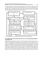
11.4.5.5 Localized electrochemical deposition
A localized electrochemical deposition apparatus is
schematically shown in Figure 11.21 [53]. The tip of a
sharply pointed electrode is placed in a plating solution
and brought near the surface where deposition is to
occur. A potential is applied between the tip and the
substrate. The electric field generated for electrodepo-
sition is then confined to the area beneath the tip, as
shown in Figure 11.21(a).
Structural material
Sacrificial
(support)
material
(g)
(e)
(f)
(d)
(a)
Substrate
Selectively
deposited 1st
material
(b)
(c)
Electrolyle
Anode
Insulator
Blanket–
depsosited
2nd material
Figure 11.20 The EFAB process: (a) electroplating through an instant mask; (b) instant-mask removal; (c) blanket deposition of
the structural material; (d) planarization by polishing; (e) repetition of electroplating, blanket deposition and planarization until the
final structure is formed; (f) remove of the sacrificial materials; (g) cross-sectional view of one layer consisting of structural material
and sacrificial materials [55]. A. Cohen, G. Zhang, F. Tseng, U. Frodis, F. Mansfeld, P. Will, EFAB: rapid, low-cost desktop
micromachining of high aspect ratio true 3-D MEMS, Proc. IEEE MEMS’ 99, ß 1999 IEEE
Polymeric MEMS Fabrication Techniques 299
In principle, truly 3-D microstructures can be formed
by using localized electrochemical deposition, provided
it is ‘electrically continuous’ with the substrate. The
spatial resolution of this process is determined by the
size of the microelectrode. Another important parameter
that needs to be considered in this process is the electro-
deposition rate. The deposition rate in this case can be
6 mm/s – two orders of magnitude greater than those of
conventional electroplating [53]. The shape and geome-
try of the microelectrode used for localized electroche-
mical deposition is critical for the deposition profile.
11.4.6 Metal–polymer microstructures
Composite metal/polymer microstructures are becoming
very popular for MEMS. A process developed in cabrera
et al. [70] allows build layer-by-layer the 3-D object so
as to obtain conductive and non-conductive parts
together, instead of manufacturing them separately and
assembling afterwards, for example, to build the cylind-
rical object described in Figure 11.22, which consists of a
metallic element (‘Part 1’) freely rotating inside a poly-
mer housing (‘Part 2’). The major steps involved in the
fabrication include the following:
Electroplating of copper to make Part 1.
‘Local’ laser silver plating on the polymer to get the
conductive base for the following.
Electroplating of copper.
Microstereolithography (MSL) with an insoluble resin
to make Part 2.
MSL with a soluble resin to make a sacrificial
structure between Parts 1 and 2.
11.5 COMBINED SILICON AND POLYMER
STRUCTURES
The MSL process can be used for fabrication of polymer
3-D microstructures, while the silicon micromachining
processes have their own advantages in circuit and
sensing and actuating element fabrication. Hence, a
combined silicon and polymeric microstructure will be
attractive for MEMS applications. Some of the research
efforts in this direction are introduced in this section.
11.5.1 Architecture combination by MSL
Architecture combination is a technology for building
complicated structures by mechanically connecting two
or more architectures made by different micromachining
processes. This approach can enable fabrication of a system
consisting of LIGA linkages driven by a Si micromotor
Fine
electrode
Deposit
Mandrel
Plating
solution
(a)
Micro stepping
motors
Stepping
motor
controller
Workstation
V
ref
Voltage
sulfamate
solution
Cu or Ni
mandrel
Pt:Ir
tip
Trigger
Current
amplifier
(b)
Figure 11.21 Localized electrochemical deposition for 3-D
micro-fabrication: (a) concept; (b) apparatus [53]. Madden, J.D.;
Hunter, I.W., ‘‘Three-dimensional microfabrication by localized
electrochemical deposition,’’ Journal of Microelectromechanical
Systems, Volume 5, Issue 1, ß 1996 IEEE
Metal
(Part 1)
(Part 2)
Air
Polymer
Figure 11.22 Complex 3-D metal–polymer part [70].
300 Smart Material Systems and MEMS
and housed in a polymer structure (Figure 11.2). Photo-
forming (its use here is the same as in MSL) is developed
for this because of its relatively high resolution and 3-D
fabrication capability (Figure 11.23(c)) [71].
Since in this approach the components fabricated with
different processes are joined together during the photo-
forming process, their proper alignment is critical to
achieve a successful architecture combination.
11.5.2 MSL integrated with thick-film lithography
Many micromechanical components have been fabri-
cated using planar processes, such as thin-film and
bulk-silicon micromachining and high-aspect-ratio
micromachining (e.g. LIGA, deep RIE and thick-resist
lithography), which have high fabrication resolutions,
but do not allow true 3-D fabrications. On the other
hand, MSL allows the building of 3-D complex micro-
structures, but with limited resolution and the problems
associated with the manipulation and assembling of
the obtained polymer structures. An approach of com-
bining MSL and thick-resist lithography may provide a
unique technique to build 3-D microstructures with
more functions [72].
11.5.3 AMANDA process
AMANDA is a process which combines surface micro-
machining, micromolding and diaphragm transfer to
fabricate micro-parts from polymers. A flexible dia-
phragm with other functional or structural materials is
deposited and patterned on a silicon substrate using a
surface micromachining process. The molding process is
then used to build the housing for the fabricated dia-
phragm and is then transferred from the silicon substrate
to the polymeric housing. Hence, the AMANDA process
Elevator driver
Elevator
Window
Laser oscillator
Resin container
Pin hole
Beam shutter
Condenser
Head driver
(a)
Micromotor
Substrate
Support
Glue mechanism
Next substrate
(b)
(1) Make a substrate with
functional elements
(2) Make glue mechanisms
by photoforming
(3) Pile up next substrate
and remove supports
(c)
Position the elevator
near the window
Scan the beam
along the first layer
Finish the first layer
Pull up the elevator
for thickness of one laye
r
Repaet these operations
to make the object shape
Figure 11.23 (a) 3-D micro-fabrication by the combined process; (b) schematic of a photoforming system; (b) process flow
for photoforming [71]. T. Takagi, and N. Nakajima, Architecture combination by micro photoforming process, Proc. IEEE MEMS 94,
ß 1994 IEEE
Polymeric MEMS Fabrication Techniques 301
allows low-cost production of reliable micro devices by
batch fabrication.
As an example for the AMANDA process, the fabri-
cation process for a pressure transducer is shown in
Figure 11.24. A silicon wafer is covered with 60 nm of
gold by PVD and then with 1.5 mm of polyimide by spin-
coating. The polyimide is patterned by photolithography
and an additional 100 nm gold is evaporated on top of the
polyimide layer. The second layer of gold is patterned
to form strain gauges. A second polyimide disk with a
thickness of 30 mm is built on these strain gauges by spin-
coating and photolithography.
The housing of AMANDA devices are produced by
molding. Typically, several housings can be fabricated in
a batch. Injection molding is generally used for the
molding in AMANDA in order to save time [73]. The
housing can be molded from thermoplastic materials
such as polysulfone, PMMA, PA, PC, PVDF or PEEK.
[73]. Mold inserts are fabricated by milling and drilling
with an CNC machine, LIGA, deep RIE, etc.
The diaphragm is then transferred into the housing. An
adhesive is injected into the cavities inside the housings.
In the example shown in Figure 11.24, the housings are
‘adhesively’ bonded to the polyimide on the wafer. The
polyimide outside the housing is cut and the housing,
together with the polyimide diaphragm, is then separated
from the wafer. The polyimide can be peeled off from the
wafer because adhesion of the first gold layer to silicon is
low. Usually, the diaphragm is encapsulated by a second
shell, which is molded and bonded similarly to the first shell.
The dimensional accuracy of the microstructures
fabricated by the AMANDA process depends on the
lithography, precision of the mold insert and molding
process and alignment and temperature control during
bonding of the molded part and diaphragm. The lateral
accuracy of the pattern on the diaphragm can be very high
because it is fabricated by photolithography. Transfer of
the diaphragm to the polymer housing causes an overall
shrinkage due to thermal expansion of the housing and the
heating for bonding. The precision of the mold insert for
housing fabrication can be very high if the LIGA process
is used. The precision of molding can be of several
microns but can be improved with injection molding or
hot-embossing molding. Disadvantages of this process are
in the alignment and control of shrinkage which affects the
dimensional accuracy of the AMANDA process [73].
REFERENCES
1. B. Zhu and V.K. Varadan, ‘Integrated MOSFET based
hydrophone device for underwater applications’, Proceed-
ings of SPIE, 4700, 101–110 (2002).
2. C.W. Hull, ‘Apparatus for production of three-dimensional
objects by stereolithography’, US Patent 4 575 330 (1984).
3. J.C. Andre
´
,A.LeMe
´
haute
´
and O. de Witte, ‘Dispositif pour
re
´
alisar un mode
`
le de pie
`
ce industrielle’, French Patent,
8 411 241 (1984).
4. H. Kodama, ‘Automatic method for fabricating a three-
dimensional plastic model with photo-hardening polymer’,
Review of Scientific Instruments, 52, 1770–1773 (1981).
Electric
contact
Fluidic contacts
Molded housings
(b)
(d)
(c)
(a)
Polyimide
Gold
Silicon wafer
Polyimide disk
Strain gauges
Adhesive
Figure 11.24 Major flow of AMANDA process; (a) a diaphragm is fabricated by silicon surface micromachining; (b) housings are
fabricated by molding or mechanical machining; (c) a diaphragm is transferred from the silicon substrate to the housing; (d) diced
chips with electric and fluidic contacts [73]. Reprinted from Sensors and Actuators A, 70, W.K.Schomburg, R. Ahrens, W. Bacher,
C. Goll, S. Meinzer, A. Quinte, AMANDA—low-cost production of microfluidic devices, pp. 153–158, Copyright 1998, with
permission from Elsevier
302 Smart Material Systems and MEMS
5. P.F. Jacobs, Rapid Prototyping and Manufacturing: Funda-
mentals of Stereolithography, Society of Manufacturing
Engineers, Dearborn, MI, USA (1992).
6. D. Kochan, Solid Freeform Manufacturing, Elsevier,
Amsterdam, The Netherlands (1993).
7. K. Ikuta, and K. Hirowatari, ‘Real three dimensional
microfabrication using stereo lithography and metal mold-
ing’, in Proceedings of IEEE: MEMS’93, IEEE, Piscataway,
NJ, USA, pp. 42–47 (1993).
8. T. Katagi and N. Nakajima, ‘Photoforming applied to fine
machining’, in Proceedings of IEEE:MEMS’93 IEEE, Pis-
cataway, NJ, USA, pp. 173–178 (1993).
9. X. Zhang, X.N. Jiang and C. Sun, ‘Micro-stereolithography
of polymeric and ceramic microstructures’, Sensors and
Actuators: Physical, A77, 149–156 (1999).
10. K. Ikuta, T. Ogata, M. Tsubio and S. Kojima, ‘Development
of mass productive micro stereo lithography (Mass-IH pro-
cess)’, in Proceedings of IEEE: MEMS’96, IEEE, Piscataway,
NJ, USA, pp. 301–305 (1996).
11. P.F. Jacobs, Stereolithography andOther RP&MTechnologies:
From RapidPrototyping toRapid Tooling, AmericanSociety of
Mechanical Engineers, New York, NY, USA (1996).
12. S. Zissi, A. Bertsch, J.Y. Jezequel, S. Corbel, J.C. Andre and
D.J. Lougnot, ‘Stereolithography and microtechnologies’,
Microsystem Technologies, 2, 97–102 (1996).
13. A. Bertsch, S. Zissi, J.Y. Jezequel, S. Corbel and J.C. Andre,
‘Microstereolithography using a liquid crystal display as
dynamic mask-generator’, Microsystem Technologies, 3,
42–47 (1997).
14. T. Nakamoto and K. Yamaguchi, ‘Consideration on the
producing of high aspect ratio micro parts using UV
sensitive photopolymer’, in Proceedings of the Seventh
International Symposium on Micro Machine and Human
Science, IEEE, New York, USA, pp. 53–58 (1996).
15. S. Monneret, V. Loubere and S. Corbel, ‘Microstereolitho-
graphy using a dynamic mask generator and a non-coherent
visible light source’, Proceedings of SPIE, 3680, 553–561
(1999).
16. L. Beluze, A. Bertsch and P. Renaud, ‘Microstereolithogra-
phy: a new process to build complex 3D objects’, Proceed-
ings of SPIE, 3680, 808–817 (1999).
17. T. Katagi and N. Nakajima, ‘Photoforming applied to fine
machining’, in Proceedings of IEEE: MEMS’93, IEEE,
Piscataway, NJ, USA, pp. 173–178 (1993).
18. K. Ikuta, S. Maruo and S. Kojima, ‘New micro stereo
lithography for freely moved 3D micro structure – super IH
process with submicron resolution’, in Proceedings of IEEE:
MEMS’98, IEEE, Piscataway, NJ, USA, pp. 290–295 (1998).
19. B.P. Wayne, Principles and Applications of Photochemistry,
Oxford University Press, Oxford, UK (1988).
20. S. Maruo and S. Kawata, ‘Two-photon-absorbed near-
infrared photopolymerization for three-dimensional micro-
fabrication, Journal of Microelectromechanical Systems, 7,
411–415 (1998).
21. K. Suzumori, A. Koga and R. Haneda, ‘Microfabrication of
integrated FMAs using stereo lithography’, in Proceedings
of IEEE: MEMS’94, IEEE, Piscataway, NJ, USA, pp. 136–
141 (1994).
22. L. Weber, W. Ehrfeld, H. Freimuth, M. Lacher, H. Lehr and
B. Pech, ‘Micro molding – a powerful tool for the large scale
production of precise microstructures’, Proceedings of SPIE,
2879, 156–167 (1996).
23. T. Hanemann, R. Ruprecht and J.H. HanBelt, ‘Micromolding
and photopolymerization’, Advanced Materials, 9, 927–929
(1997).
24. L. Lin, C J. Chiu, W. Bache and M. Heckele, ‘Microfab-
rication using silicon mold insert and hot embossing’, in
MHS’96, Proceedings of the Seventh International Sympo-
sium Micro Machine and Human Science, IEEE, Piscataway,
NJ, USA, pp. 67–71 (1996).
25. J. Akedo, M. Ichiki, K. Kikuchi and R. Maeda, ‘Fabrication
of three-dimensional micro structure composed of different
materials using excimer laser ablation and jet molding’, in
Proceedings of the IEEE: The Tenth Annual International
Workshop on Micro electro Mechanical Systems, IEEE,
Piscataway, USA, pp. 135–140 (1997).
26. Y. Xia and G.M. Whitesides, ‘Soft lithography’, Angewandte
Chemie; International Edition, 37, 350–375, (1998).
27. X M. Zhao, Y. Xia and G.M. Whitesides, ‘Fabrication of
three-dimensional micro-structures: microtransfer molding’,
Advanced Materials, 8, 837–840 (1996).
28. E. Kim, Y. Xia and G.M. Whitesides, ‘Polymer microstruc-
ture formed by moulding in capillaries’, Nature (London),
376, 581–584 (1995).
29. E. Kim, Y. Xia, X M. Zhao and G.M. Whitesides, ‘Solvent-
assisted microcontact molding: a convenient method for
fabricating three-dimensional structures on surfaces of
polymers’, Advanced Materials, 9, 651–654 (1997).
30. Y. Hirata, H. Okuyama, S. Ogino, T. Numazawa and H.
Takada, ‘Piezoelectric composites for micro-ultrasonic
transducers realized with deep-etch X-ray lithography’, in
Proceedings of IEEE: MEMS’95, IEEE, Piscataway, NJ,
USA, pp. 191–196 (1995).
31. S.N. Wang, J F. Li, R. Toda, R. Watanabe, K. Minami and
M. Esashi, ‘Novel processing of high aspect ratio 1–3
structures of high density PZT’, in Proceedings of IEEE:
MEMS’98, IEEE, Piscataway, NJ, USA, pp. 223–228
(1998).
32. W. Bacher, W. Menz and J. Mohr, ‘The LIGA technique and
its potential for microsystems — a survey’, IEEE Transac-
tions: Industrial Electronics, 42, 431–441 (1995).
33. J.Elders, H.V. Jansen, M. Elwenspoek and W. Ehrfeld,
‘DEEMO: a new technology for the fabrication of micro-
structures’, in Proceedings of IEEE: MEMS’95, IEEE,
Piscataway, NJ, USA, pp. 238–243 (1995).
34. H. Freimuth, V. Hessel, H. Koelle, M. Lacher, W. Ehrfeld, T.
Vaahs and M. Brueck, ‘Formation of complex ceramic
miniaturized structures by pyrolysis of poly(vinylsilazane),
Journal of the American Ceramics Society, 79, 1457–1465
(1996).
35. V. Piotter, T. Benzler, T. Hanemann, H. Wollmer, R.
Ruprecht and J. Hausselt, ‘Innovative molding technologies
Polymeric MEMS Fabrication Techniques 303
for the fabrication of components for microsystems, Pro-
ceedings of SPIE, 3680, 456–463 (1999).
36. Website: [ />htm].
37. H. Becker and U. Heim, ‘Silicon as tool material for polymer
hot embossing’, in Proceedings of IEEE: MEMS’99, IEEE,
Piscataway, NJ, USA, pp. 228–231 (1999).
38. O. Kemmann, C. Schaumburg and L. Webber, ‘Micro
moulding behavior of engineering plastics’, Proceedings
of SPIE, 3680, 464–471, (1999).
39. L. Weber, W. Ehrfeld, M. Begemann, U. Berg and F. Michel,
‘Fabrication of plastic microparts on wafer level’, Proceed-
ings of SPIE, 3874, 44–52 (1999).
40. W.S. Beh, I.T. Kim, D. Qin, Y. Xia and G.M. Whitesides,
‘Formation of patterned microstructures of conducting
polymers by soft lithography and applications in microelec-
tronic device fabrication’, Advanced Materials, 11, 1038–
1041 (1999).
41. J.M. English and M.G. Allen, ‘Wireless micromachined
ceramic pressure sensors’, in Proceedings of IEEE:
MEMS’99, IEEE, Piscataway, NJ, USA, pp. 511–516 (1999).
42. A.H. Epstein, S.D. Senturia, G. Ananthasuresh, A. Ayon, k.
Breuer, K S. Chen, F. Ehrich, G. Gauba, R. Ghodssi, C.
Groshenry, S. Jacobson, J. Lang, C C. Mehra, J. Mur
Miranda, S. Nagle, D. Orr, E. Piekos, M. Schmidt, G.
Shirley, S. Spearing, C. Tan, Y S. Tzeng and I. Waitz,
‘Power MEMS and ‘Power MEMS and microengines’, in
Proceedings of Transducers’97: International Conference
on Solid State Sensors and Actuators, Vol. 2(2), IEEE,
Piscataway, NJ, USA, pp. 753–756 (1997).
43. H.H. Bau, S.G.K. Ananthasuresh, J. J. Santiago-Aviles, J.
Zhong, M. Kim, M. Yi, P. Espinoza-Vallejos and L.
Sola-Laguna, ‘Ceramic tape-based meso systems tech-
nology’, in Proceedings of the ASME International
Mechanical Engineering Congress and Exposition on Micro-
Electro-Mechanical Systems (MEMS), ASME, New York,
NY, USA, pp. 491–498 (1998).
44. D.L. Polla and L.F. Francis, ‘Ferroelectric thin films in
microelectromechanical systems applications’, MRS Bulle-
tin, 59–65 (July 1996).
45. V.K. Varadan, V.V. Varadan and S. Motojima, ‘Three-
dimensional polymeric and ceramic MEMS and their appli-
cations’, Proceedings of SPIE, 2722, 156–164 (1996).
46. B.C. Mutsuddy and R.G. Ford, Ceramic Injection Molding,
Chapman & Hall, London, UK (1995).
47. R.M. German, and A. Bose, Injection Molding of Metals and
Ceramics, Metal Powder Industries Federation, Princeton,
NJ, USA (1997).
48. R. Roy, D. Agrawal, J. Cheng and S. Gedevanishvili, ‘Full
sintering of powdered-metal bodies in a microwave field’,
Nature (London), 399, 668–670 (1999).
49. W. Bartusch, P. Mehringer and G.A. Muller, ‘Microwave
sintering – from the laboratory to industrial scale’, Kera-
mische Zeitschrift, 50, 810–817 (1998).
50. X.N. Jiang, C. Sun, X. Zhang, B. Xu and T.H. Ye, ‘Micro-
stereolithography of lead zirconate titanate thick film on
silicon substrate’, Sensors and Actuators: Physical, 87A,
72–77 (2000).
51. X. Zhang, X.N. Jiang and C. Sun, ‘Micro-stereolithography
for MEMS, in Proceedings of the ASME International
Mechanical Engineering Congress and Exposition on
Micro-Electro-Mechanical Systems (MEMS), ASME New
York, NY USA, pp. 3–9 (1998).
52. M.L. Griffith, and J.W. Halloran, ‘Stereolithography of
ceramics’, in Proceedings of the 27th International
SAMPE Technical Conference, SAMPE, Covina, CA,
USA, pp. 970–979 (1995).
53. T. Benzler, V. Piotter, T. Hanemann, K. Mueller, P. Norajitra,
R. Ruprecht and J. Hausselt, ‘Innovations in molding
technologies for microfabrication’, Proceedings of SPIE,
3874, 53–60 (1999).
54. J.D. Madden and I.W. Hunter, ‘Three-dimensional micro-
fabrication by localized electrochemical deposition’, Jour-
nal of Microelectromechanical Systems, 5, 24–32 (1996).
55. A. Cohen, G. Zhang, F. Tseng, U. Frodis, F. Mansfeld and P.
Will, ‘EFAB: rapid, low-cost desktop micromachining of
high aspect ratio true 3-D MEMS’, in Proceedings of IEEE:
MEMS’99, IEEE, Piscataway, NJ, USA, pp. 244–251 (1999).
56. C.S. Taylor, P. Cherkas, H. Hampton, J.J. Frantzen, B.O.
Shah, W.B. Tiffany, L. Nanis, P. Booker, A. Salahieh and R.
Hansen, ‘A spatial forming – a three dimensional printing
process’, in Proceedings of IEEE: MEMS’94, IEEE, Piscat-
away, NJ, USA, pp. 203–208 (1994).
57. Y.P. Kathuria, ‘Rapid prototyping: an innovative technique
for microfabrication of metallic parts’, in Proceedings of the
Seventh International Sympossium on Micro Machine and
Human Science, IEEE, Piscataway, NJ, USA, pp. 59–65
(1996).
58. J.B. Mohler and H.J. Sedusky, Electroplating for the Metal-
lurgist, Engineer and Chemist, Chemical Publishing Co.,
Inc., New York (1951).
59. W. Blum and G.B. Hogaboom, Principles of Electroplating
and Electroforming, McGraw-Hill, New York, NY, USA
(1949).
60. L.T. Romankiw, ‘A path from electroplating through litho-
graphic masks in electronics to LIGA in MEMS’, Electro-
chimica Acta, 42, 2985–3005 (1997).
61. R.J. von Gutfeld and K.G. Sheppard, ‘Electrochemical
microfabrication by laser-enhanced photothermal pro-
cesses’, IBM Journal of Research and Development, 42,
639–653 (1998).
62. E.W. Becker, W. Ehrfeld, P. Hagmann, A. Maner and D.
Muenchmeyer, ‘Fabrication of microstructures with high
aspect ratios and great structural heights by synchrotron
radiation lithography, galvanoforming and plastic moulding
(LIGA process)’, Microelectronic Engineering, 4, 35–56
(1986).
63. A.B. Frazier and M.G. Allen, ‘Metallic microstructures fabri-
cated using photosensitive polyimide electroplating molds’,
Journal of Microelectromechanical Systems, 2, 87–94 (1993).
64. J M. Quemper, S. Nicolas, J.P. Gilles, J.P. Grandchamp, A.
Bosseboeuf, T. Bourouina and E. Dufour-Gergam, ‘Permal-
304 Smart Material Systems and MEMS
loy electroplating through photoresist molds’, Sensors and
Actuators: Physical, A74,1–4, (1999).
65. B. Loechel, A. Maciossek, H.J. Quenzer and B. Wagner,
‘Ultraviolet depth lithography and galvanoforming for
micromachining’, Journal of Electrochemical Society, 143,
237–244 (1996).
66. Y. Konaka and M.G. Allen, ‘Single- and multi-layer elec-
troplated microaccelerometers’,inProceedings of IEEE:
MEMS’96, IEEE, Piscataway, NJ, USA, pp. 168–173 (1996).
67. J B. Yoon, B.K. Kim, C.H. Han, E. Yoon and C.K. Kim,
‘Surface micromachined solenoid on-Si and on-glass induc-
tors for RF applications’, IEEE Electron Device Letters, 20,
487–489 (1999).
68. C.H. Ahn and M.G. Allen, ‘Micromachined planar inductors
on silicon wafers for MEMS applications’, IEEE Transac-
tions : Industrial Electronics, 45, 866–876 (1998).
69. Q. Lin, K.G. Sheppard, K.G. M. Datta and L.T. Romankiw,
‘Laser-enhanced electrodeposition of lead–tin solder’,
Journal of the Electrochemical Society, 139,L62–L63
(1992).
70. M. Cabrera, A. Bertsch, J. Chassaing, J.Y. von Jezequel and
J. C. Andre, ‘Microphotofabrication of very small objects:
pushing the limits of stereolithography’, Molecular Crystals
and Liquid Crystals, 315, 223–234 (1998).
71. T. Takagi and N. Nakajima, ‘Architecture combination by
micro photoforming process’,inProceedings of IEEE:
MEMS’94, IEEE, Piscataway, NJ, USA, pp. 211–216
(1994).
72. A. Bertsch, H. Lorenz and P. Renaud, ‘Combining micro-
stereolithography and thick resist UV lithography for 3D
microfabrication’,inProceedings of IEEE: MEMS’98,
IEEE, Piscataway, NJ, USA, pp. 18–23 (1998).
73. W.K. Schomburg, R. Ahrens, W. Bacher, C. Goll, S. Meinzer
and A. Quinte, ‘AMANDA – low-cost production of micro-
fluidic devices’, Sensors and Actuators, A70, 153–158
(1998).
Polymeric MEMS Fabrication Techniques 305
12
Integration and Packaging of Smart
Microsystems
12.1 INTEGRATION OF MEMS
AND MICROELECTRONICS
The integration of an MEMS sensor with electronics has
several advantages when dealing with small signals. The
function of electronics is to make sure that the MEMS
components operate correctly. The state-of-the-art in
MEMS is combination with ICs, utilizing advanced
packaging techniques to create a system-on-a-package
(SOP) or a system-on-a-chip (SIP) [1]. However, in such
cases it is important that the process used for MEMS
fabrication does not adversely affect the electronics.
MEMS devices can be fabricated as pre- or post-proces-
sing modules, which are integrated by standard proces-
sing steps. The choice of integration depends on the
application and different aspects of its implementation
technology. Various approaches for their integration with
microelectronics are considered in this section.
In general, three possibilities exist for monolithic
integration of CMOS and MEMS: (a) CMOS first, (b)
MEMS in the middle, and (c) MEMS first [2,3]. In
addition, a hybrid approach, known as a multichip
module is also used often for such integration. Each of
these methods has its own advantages and disadvantages.
A comparison is listed in Table 12.1. It may be recalled
that a number of materials, such as ceramics, are used in
the fabrication of various MEMS, unlike in CMOS.
Annealing of polysilicon or sintering of most ceramics
generally require higher processing temperatures, often
exceeding that allowed in CMOS. For example, at
temperatures in excess of about 800
C, aluminum metal-
lizations may diffuse and cause performance degrada-
tion. Hence, if ceramic processing at a higher
temperature is involved, it may be preferable to fabricate
the MEMS first. In contrast, if the MEMS involves
delicate structures, several common CMOS processes,
such as ‘lift off’, may degrade the MEMS performance.
Hence, the choice of process sequence is highly depen-
dent on the particular MEMS structure at hand.
12.1.1 CMOS first process
In this approach, first developed at UC Berkeley, the
temperature limitation due to aluminum is eliminated by
using tungsten as the conducting layer [4]. In this
process, known as ‘modular integration of CMOS with
microstructures’ (MICSs), CMOS circuits are first fabri-
cated using conventional processes, and polysilicon
microstructures are then fabricated on the top after
passivating with SiN and using a phosphosilicate glass
(PSG) sacrificial layer. Rapid thermal annealing (RTA) of
polysilicon in nitrogen at 1000
C for ‘stress relief’ does
not affect the CMOS performance. A cross-sectional
view of the device is shown in Figure 12.1. In an
alternate approach, MEMS fabrication is limited to
below 400
C so that these steps do not adversely affect
the CMOS fabricated first. Some examples of successful
microsystems fabricated by this approach as listed in
Table 12.2.
12.1.2 MEMS first process
In the method, MEMS structures are first fabricated on
the silicon wafer [12,13]. The primary advantage is that
higher processing temperature can be used to achieve
better process optimization. In this process, developed at
the Sandia National Laboratories, shallow trenches are
first anisotropically etched on the wafer and the MEMS is
Smart Material Systems and MEMS: Design and Development Methodologies V. K. Varadan, K. J. Vinoy and S. Gopalakrishnan
# 2006 John Wiley & Sons, Ltd. ISBN: 0-470-09361-7
built within these trenches [14]. Silicon nitride and
sacrificial oxide may be deposited within these trenches
for the MEMS structures. A polysilicon layer on top of
these layers helps establish contacts with the subsequent
CMOS processing. Chemical–mechanical planarization
(CMP) and high-temperature annealing are done to
optimize this polysilicon layer. The sacrificial oxide
covering the MEMS structure is removed after fabrica-
tion of the CMOS device. A photoresist is used as a
protective layer during the release process. A cross-
sectional view of a typical device fabricated with this
process in shown in Figure 12.2. Some examples of
successful microsystems fabricated by this approach are
listed in Table 12.3.
12.1.3 Intermediate process
The simplest form of an integrated MEMS device is where
the existing layers for fabricating the IC are used for the
mechanical components in MEMS [17–19]. Standard
microelectronics processes require a number of layers on
top of the wafer, such as oxide, polysilicon, metal and
nitride. Utilizing these layers in an MEMS requires only a
few additional steps of masking and etching, as explained
in Figure 12.3. Some examples of successful microsys-
tems fabricated by this approach are listed in Table 12.4.
12.1.4 Multichip module
The incompatibilities in the fabrication processes of
MEMS and ICs have made their monolithic integration
difficult. Multichip module (MCM) packaging provides
an efficient solution to integrate MEMS with microelec-
tronic circuits as it supports a variety of die types in a
common substrate without the need for resorting to
significant changes in the fabrication process of either
component. Several sensors, actuators or a combination
can be combined in a single chip using the MCM
technique [22]. Using this approach, both surface- and
bulk-micromachined components may be integrated with
the electronics. When using this approach, separate
procedures are required for releasing and assembling
the MEMS structures without degrading the package or
other dies in the module.
Several variants of this approach exist: high-density
interconnect (HDI), chip-on-flex (COF) and micro-module
system (MMSs) MCM-D. These are compared in
Tungsten
metallization
Gate
poly
TiN/TiSi
2
Poly-poly
capacitor
PSG
Nitride
passivation
Poly 2
Poly 1
n
+
n
+
N Substrate
P well
p
+
p
+
Figure 12.1 Cross-sectional view of a device fabricated with the MICS process [4]. W. Yun; Howe, R.T.; Gray, P.R., ‘‘Surface
micromachined, digitally force-balanced accelerometer with integrated CMOS detection circuitry,’’ 5th Solid-State Sensor and
Actuator Workshop, 1992. Technical Digest, # 1992 IEEE
308 Smart Material Systems and MEMS
Publisher's Note:
Permission to reproduce this image
online was not granted by the
copyright holder. Readers are kindly
requested to refer to the pr
in
ted v ersion
of this chapter.
Table 12.5. In standard HDI process the dies are embedded
in cavities milled on the base substrate and then a thin-film
interconnecting layer is deposited on top of the compo-
nents. Holes for the interconnecting vias are made by laser
ablation using a 350 nm argon ion laser. Physical access to
the MEMS die is provided by an additional laser ablation
step. Figure 12.4(a) shows a typical HDI process flow,
compared with an augmented HDI process for MEMS
Table 12.2 Examples of the CMOS first approach for the fabrication of microsystems [5].
Organization Microsystem Remarks Reference
UC Berkeley Micro- Tungsten metallization to [4]
accelerometer increase temperature limit of
CMOS; by MICS process
Texas Instruments Digital An array of aluminum [6]
micro-mirror micro-mirrors integrated over a
static random access memory
University of Michigan/ Gyroscope — [7]
Delphi Automotive
Systems
University of Acceleration MEMS parts built by additive [8]
Bremen/Infineon switch electroplating technology
Honeywell Infrared SiN encapsulation of emitter [9]
thermal for electrical isolation and
imager mechanical support
Stanford Biosensor with A hybrid glass/PDMS/silicon [10]
University disposable chamber in a cell cartridge
cartridges that includes fluidic interchanges,
physiological sensors and
environmental regulation
Austrian Micro Capacitive Wafer bonding of a [11]
Systrems acceleration polysilicon sensor wafer
sensor with a CMOS substrate
p
-tub
N
-tub
Sec oxide
CMOS device area
Micromechanical device area
Poly 2
Poly 1
n-type silicon substrate
Nitride
Nitride
Arsenic-doped epitaxial layer
MM poly 0
PETEOS
Fiell oxide
TFOF
Ped
TEOF
Field Oxide
PE nitride
Pad
Figure 12.2 Cross-sectional view of a typical device fabricated with an MEMS –first fabrication process developed at the Sandia
National Laboratories [14]. J.H. Smith, S. Montague, J.J. Snieowski, J.R. Murray, and P.J. McWhorter, ‘‘Embedded micromechanical
devices for monolithic integration of MEMS with CMOS,’’ IEDM’95 Tech. Digest, # 1995 IEEE
Integration and Packaging of Smart Microsystems 309
packaging (Figure 12.4(b)) by an additional laser-ablation
step to allow physical access to the MEMS die. The
windows in the dielectric overlay above the MEMS device
are selectively etched used laser ablation. COF is a lower-
cost variant of HDI in which a molded plastic substrate
replaces the ceramic.
In the MCM-D approach, the interconnected layers are
deposited on the substrate and the dies are mounted
above these. Interconnection between the dies and the
packaging is done by wire bonding. Most of the common
wet-etching techniques are not suitable for bulk micro-
machining of structures while following this approach.
Hence, isotropic dry etching using XeF
2
can be used for
selectively etching silicon. Wet etching using HF can,
however, be used for releasing the surface-micromachined
structure parts of this chip after shielding the bulk micro-
machined parts by a positive photoresist.
The main disadvantage of the MCM approach is the
possibility for signal degradation due to parasitic effects
between the components and the apparent added packag-
ing expenses.
12.2 MEMS PACKAGING
Packaging is the science of establishing interconnections
between the various subsystems and providing an appro-
priate operating environment for the electromechanical
circuits to process the gathered information. The disci-
pline of microelectromechanical systems (MEMS) was
developed so closely with silicon processing that most
of the early packaging technologies for MEMS were
directly adapted from microelectronics. However, in
contrast to the case of microelectronics, most MEMS
devices need a physical access to the outside world,
Table 12.3 Examples of the MEMS first approach for the fabrication of microsystems [5].
Organization Microsystem Remarks Reference
Sandia National — Microstructures embedded [14]
Laboratories below the CMOS by an integrated
MEMS (iMEMS) process
Physical Trench–Hall Hard mask, consisting of [15]
Electronics device SiO
2
/SiN/SiO
2
,isfirst
Laboratory,Zurich/ deposited for etching trenches
Infineon and apolysilicon layer for
electrical shielding
Microsystems Pressure sensor Micromachined parts are added [16]
Technology and angular to the CMOS fabricated parts by
Laboratory, MIT rate sensor wafer fusion bonding
Circuit
(a) (b)
(c) (d)
Acceleration sensor
n-silicon p-welln-well
Passivation
Aluminium
photoresist
Silicon dioxide
n-doped Polysilicon
Silicon nitride
Sacrificial layer
n
+
doped silicon p
+
doped silicon
Siesmic mass
Suspension
Anchor
Figure 12.3 Integration of surface micromachining with CMOS [17]. Hierold, C, Hildebrandt, A, Naher, U, Scheiter, T, Mensching,
B, Steger, M, Tielert, R. ‘‘A pure CMOS surface micromachined integrated accelerometer,’’ The 9th Annual Intl Workshop on Micro
Electro Mechanical Systems, 1996, MEMS ’96, Proceedings. IEEE, 11–15 Feb, # 1996 IEEE
310 Smart Material Systems and MEMS
either to mechanically react with an external parameter
or to sense a physical variable. In state-of-the art micro-
electronics, the device normally accesses the outside
world via electrical connections alone and the systems
are totally sealed and isolated. Therefore, unlike electro-
nic packaging, where a standard package can be used for
a variety of applications, MEMS packages tend to be
customized.
Challenges in the design of packaging depend on the
overall complexity of the ultimate application of the
device. However, there are no sharp boundaries between
these classes. The size of the package, choice of its shape
and material, alignment of the device, mounting for the
isolation of shock and vibration and sealing are some of
the many concerns in MEMS packaging. Considerations
in packaging may be different, depending on whether the
device is used as an MOEMS, RF MEMS or simpler
sensors or actuators. Furthermore, special considerations,
such as biocompatibility, may have to be examined when
designing the packaging of a system. Many important
lessons that have been learned throughout years of
experience in the microelectronics industry could be
adapted to the packaging of MEMS devices.
In MEMS, mechanical structures and electrical com-
ponents are combined to form a functional system. While
packaging, these electrical and mechanical components
are interconnected and the electrical inputs are interfaced
with external circuits. MEMS components can be extre-
mely fragile and must be protected from mechanical
damage and hostile environments. This section presents
the fundamentals of microelectronic packaging adapted
for MEMS technology.
12.2.1 Objectives in packaging
The objective of packaging is to integrate all components
of a system such that cost, mass and complexity are
minimized. The MEMS package should protect the
device, while at the same time letting it perform its
intended functions with less attenuation of signal in a
given environment [23,24]. Packaging is an expensive
process since it seeks to protect relatively fragile struc-
tures integrated into the device. For a standard integrated
circuit, the packaging process may take up to 95 % of the
total manufacturing cost. Issues in MEMS packaging are
more difficult to solve due to stringent requirements in
processing and handling and the diversity and fragile
nature of the microstructures.
MEMS packages provide a mechanical support, an
electrical interface to the other system components and
protection from the environment. In addition, packages
should also provide an interface between the system and
the physical world. Many of the MEMS sensors often
require an interface between the sensing media and the
sensing area. For example, a pressure-sensor packaging
requires incorporation of a pressure port to transmit fluid
pressure to the sensor. This makes the major difference
between the standard semiconductor device packages and
the MEMS packages.
12.2.1.1 Mechanical support
Once the MEMS devices are wire-bonded and other
electrical connections are made, the assembly must be
protected by covering the base or by encapsulating the
assembly in plastic or ceramic materials and the electrical
connections are usually made through its walls. If the
packaging creates excessive stress in the sensing structure,
it can cause a change in device performance. Managing
package-induced stress in the device becomes important
for MEMS package design. With most MEMS being
mechanical systems, protection and isolation of such
Table 12.4 Examples of the intermediate approach
for the fabrication of microsystems [5].
Organization Microsystem Reference
Analog Devices Accelerometer [20]
Infineon Pressure sensor [21]
Table 12.5 A comparison of various MCM
technologies [22]. Butler J.T., Bright V.M., Chu P.B.
and Saia R.J., Adapting Multichip module foundries
for MEMS packaging, Proc of IEEE International
Conf on Multichip modules and High density
Packaging, # 1998 IEEE
Property MCM-D HDI
Substrate Aluminum Alumina
Dielectric material Polyimide Kapton
Conductor Copper Ti/Cu/Ti
metallization
Die-interconnection Wire Direct
method bond metallization
Maximum operating 100–400 >1 GHz
frequency MHz
Requirement None Additional laser
for process ablation required
modifications for open access
to MEMS dies.
Integration and Packaging of Smart Microsystems 311
devices from thermal and mechanical shock, vibration,
acceleration and other physical damages during their
operation is critical to their performance. The mechanical
stress affecting a system depends on the application. For
example, the device package for a military aircraft is
different from those used in communication satellites.
The coefficient of thermal expansion of the package
material should be equal to that of silicon for reliability
because the thermal cycle may cause cracking or delami-
nation if they are unmatched.
12.2.1.2 Electrical interface
The connection between the MEMS and the signal lines
is usually made with wire bonds or flip-chip die attach-
ments and multilayer interconnections. Wire bonds and
other electrical connections to the device should be made
with care taken to protect the device from scratches and
other physical damages. DC and RF signals to the
MEMS systems are given through these connections
and interfaces. In addition, these packages should be
able to distribute signals to all components within the
package. Examples of the external interfaces required
when packaging variuos types of devices are shown in
Table 12.6.
12.2.1.3 Protection from environment
Many of the MEMS devices and sensors are designed to
measure variables from the surrounding environment.
MEMS packages must protect the micromachined parts
from the environment and at the same time it must
provide interconnections to electrical signals, as well as
access to and interaction with the external environment.
The hermetic packaging generally useful in microelec-
tronic devices is not suitable in such MEMS devices.
These devices might be integrated with the circuits or
mounted on a circuit board. Special attention in packa-
ging can protect a micromachined device from aggres-
sive surroundings and mechanical damage. Elements that
cause corrosion or physical damage to the metal lines as
well as other components, such as moisture, remain a
concern for many MEMS devices. Moisture may be
introduced into the package during fabrication and before
sealing can damage the materials. For example, alumi-
num lines can corrode quickly in the presence of moist-
ure. Junctions of dissimilar metals can also corrode in the
presence of moisture.
Hermetic MEMS packages provide good barriers to
liquids and gases. In hermetic packages, the electrical
interconnections through a package must confirm her-
metic sealing. Wire bonding is the popular technique to
electrically connect the die to the package. Bonding of
gold wires is easier than bonding aluminum wires. The
use of wire bonding has serious limitations in MEMS
packaging due to the application of ultrasonic energy at
Mill substrate and attach die
Bond pads
Substrate
Substrate
Substrate
Substrate
Die
Die
Die
Die
Die
Die
Die
Die
MEMS
CMOS
Apply dielectric layer and laser drill vias
Dielectric
Sputter metallization and apply next dielectric layer
Metal
Laser-ablated windows for MEMS access
(a)
(b)
Figure 12.4 (a) HDI process; (b) MEMS access in the HDI
process [22]. Butler J.T., Bright V.M., Chu P.B. and Saia R.J.,
Adapting Multichip module foundries for MEMS packaging,
Proc of IEEE International Conf on Multichip modules and High
density Packaging, # 1998 IEEE
Table 12.6 External interfaces required when
packaging various types of devices.
Device Electrical Non-electrical
interface interface
Microelectronics Input/ —
Output
MEMS sensors Output Fluid channels
(gas/liquid)
Physical contact
(pressure/temperature)
None (navigational)
MEMS actuators Control Fluid channels
(micro pump)
RF-MEMS Control RF cables/connectors
MOEMS Control Optical fibers/couplers
312 Smart Material Systems and MEMS
a frequency between 50 to 100 kHz as these frequencies
may stimulate oscillations by the microstructures. Since
most microstructures have resonant frequencies in the
same range, the chance of structural failure during the
wire bonding is high [25].
In most spaceborne applications, parts are hermetically
sealed due to the perceived increase in reliability and to
minimize the outgassing. When epoxies or cyanate esters
are used to attach the die, they outgas while curing.
Outgassing is a concern for many devices since these
particles could be deposited on the components, hence
degrading their performance. This leads to ‘stiction’ and
corrosion of the device. Die-attachment materials with a
low Young’s modulus allow the chip to move during the
ultrasonic wire bonding, so resulting in low bond
strength.
12.2.1.4 Thermal considerations
MEMS devices used for present-day applications do not
have a high-power-dissipation requirement. The thermal
dissipation from MEMS devices is not a serious problem
since the temperature of the MEMS devices usually does
not increase substantially during operation. However, as
the integration of MEMS with other high-power devices,
such as amplifiers, in a single package increases, the need
for heat dissipation arises to ensure proper operations of
these devices. Thus, thermal management is an important
consideration in package design.
Heat-transfer analysis and thermal management beco-
me more complex by packaging different functional
components into a tight space. This miniaturization
also raises issues such as coupling between the system
configurations and the overall heat dissipation to the
environment. The configuration of the system shell
becomes important for heat dissipation from the system
to the environment [26,27]. Heat spreading in the thin
space is one of the most important modes of heat transfer
in compact electronic equipment and microsystems. As
the system shrinks, the space available for installation of
a fan or pump inside the system shell disappears and the
generated heat has to be dissipated through the shell to
the surrounding environment. In general, the primary
motives in heat-transfer design are to diffuse heat as
rapidly as possible and to maximize the heat dissipation
from the system shell to the environment.
12.2.2 Special issues in MEMS packaging
Although it follows a similar path as microelectronics
packaging, the design of MEMS packages does need to
address several unique challenges. Some of these, as well
as their typical solutions, are described in the following
paragraphs.
12.2.2.1 Release of structures
During the fabrication of MEMS polysilicon structures
by surface micromachining techniques, these are pro-
tected against damage or contamination by silicon diox-
ide layers. In order to release these polysilicon structures,
the oxide layers should be etched out, often by HF
solution. The issue here is the timing of this release
etch, vis-a
`
-vis the packaging. If this is done before the
start of packaging, it may weaken the structure, but if
done during or after packaging, there is scope for con-
tamination and incompatibility issues. Another asso-
ciated risk is stiction – a phenomenon by which
microstructures tend to stick to one another after release.
This is caused by capillary action of the droplets of the
rinse solutions used after etching and may be reduced by
incorporating ‘dimples’ into the structures. Other solu-
tions, such as freeze drying and critical CO
2
drying, are
also useful to reduce stiction after release. To further
reduce the possibilities of stiction during the lifetime of
the device, non-stick dielectric films may be inserted
during the fabrication process.
12.2.2.2 Die separation
‘Dicing’ is a common process used in microelectronics
fabrication for separating mass-produced devices. The
current standard die-separation method adopted for silicon
is to cut the wafer by using a diamond-impregnated blade.
The blade and the wafer are ‘flooded’ with high-purity
water while the blade spins at 45 000 rpm. This creates no
problem for standard ICs because the surface is essentially
sealed to the effects of water and silicon dust. However, if
a released MEMS device is exposed to water and debris,
the structures may break off or get clogged and the
moisture may adversely affect their performance. Efforts
to protect these surfaces with photoresist and other coat-
ings have provided only limited success. Another possi-
bility is to delay the release of the structures to until after
the dicing. An alternate process called wafer cleaving,
used in III–IV semiconductor lasers, may also be useful in
MEMS die separation [3].
12.2.2.3 Die handling
During automated processes, vacuum pick-up heads are
commonly used in handling the die in microelectronics.
Integration and Packaging of Smart Microsystems 313
As these may not be used for MEMS devices, due to the
presence of delicate structures, additional clamp attach-
ments are required to handle the MEMS die, possibly by
their edges. However, the requirement for this special
equipment may be eliminated by wafer level encapsula-
tion. In this approach, a capping wafer is used during
dicing, such that each MEMS chip has a protective chip
attached to it. These wafers are bonded by using direct
binding or anodic bonding. However, the additional
process steps required may cause an increase in the
cost of the device.
12.2.2.4 Interfacial stress
Thermal annealing is required for MEMS structures
fabricated with polysilicon. There are several other
processes during packaging of the device (such as the
use of hard solders for die attachments, package lid
sealing, etc.) that may introduce additional thermal
stress. The application of high temperatures for these
purposes on a complex structure, such as MEMS invol-
ving several materials with varying coefficients of ther-
mal expansion (CTEs) may result in device deformation,
misalignment of parts, change in the resonant frequencies
of the structures and ‘buckle’ in long beam elements.
Lower-moduli die-attach materials may solve these pro-
blems to a limited extent but may introduces additional
complications, such as ‘creep over time’ [3]. They may
also allow the chip to move during wire bonding, so
resulting in low bond strength.
12.2.2.5 Control of outgassing
Many die-attachment materials outgas during their cur-
ing. These vapors and moisture may deposit on structures
and cause stiction or corrosion and may result in degra-
dation of performance. The solution may include using
low-outgassing materials and/or the removal of outgas-
sing vapors during the die-attachment curing process.
12.2.3 Types of MEMS packages
Although MEMS represent a relatively new topic, the
methods of packaging of very small mechanical devices
are not new. For example, the aerospace and watch
industries have been performing this task for a very
long time. However, MEMS applications usually require
specialized package designs, depending on the applica-
tion and optimization procedures. In general, the possible
group of packages for MEMS can be categorized into
metal, ceramic, plastic and multilayer packages.
12.2.3.1 Metal packages
Metal packages are often used in MMIC and hybrid
circuits due to their thermal dissipation and electromag-
netic shielding effectiveness. In addition, these packages
are sufficiently rugged, especially for larger devices.
Hence, these are also often preferred for MEMS applica-
tions. Materials like CuW (10/90), Silver
TM
(Ni–Fe
alloy), CuMo (15/85) and CuW (15/85) are good thermal
conductors and have higher coefficients of thermal
expansion (CTEs) than silicon.
A ‘baking’ step is performed before the final assembly
in order to remove trapped gas and moisture, thus
reducing the possibility of corrosion. Au–Sn solders are
preferred since these are especially suited when joining
dissimilar materials. An alternate method is to use weld-
ing by localized heating methods, such as by the use of
lasers. The primary limitation of these packages is the
presence of the glass or ceramic ‘feedthroughs’, as these
may be brittle if not handled properly.
12.2.3.2 Ceramic packages
Ceramic packaging is one of the most common types
used in the microelectronics industry, due to its features
such as low mass, low cost and easy mass production.
The ceramic packages can be made hermetic, adapted to
multilayer designs and be easily integrated for the signal-
‘feedthrough’ lines. Multilayer packages reduce the size
and cost of integration of multiple MEMS into a single
package. The electrical performances of the packages
can be tailored by incorporating multilayer ceramics and
‘interconnect’ lines.
Co-fired multilayered ceramic packages are con-
structed from individual ‘green’ pieces of thin films.
Metal lines are deposited in each film by thick-film
processing, such as screen printing, and via holes for
the interconnections to be drilled. The unfired layers are
then stacked and aligned and laminated together by firing
at high temperatures. MEMS and the necessary compo-
nents are then attached using epoxy or solders and wire
bonds are made.
There are several problems associated with the cera-
mic packaging. The ‘green state’ shrinks during the firing
process and the amount of shrinkage depends on the
number of via holes (and hence may be different in each
layer.) The ceramic-to-metal adhesion is not as strong as
the ceramic-to-ceramic adhesion. The processing tem-
peratures of ceramics limit the choice of metal lines as
the metal may react with ceramics at high temperatures.
In such cases, metals used are W and Mo are employed
but if low-temperature ‘co-fired’ ceramics (LTCCs) are
314 Smart Material Systems and MEMS
used, the most frequently used metal lines are Ag, Au
and Au–Pt.
12.2.3.3 Thin-film multilayer packages
This method of packaging uses layers of thin films of
polyimide instead of the ceramics described above.
These, having lower dielectric constants result in lower
line capacitances (faster circuits) and less line-to-line
couplings (miniaturization). These packages may be put
together by individually processing thick (25 mm) poly-
imide sheets or by spin-coating polyimide thin films on a
substrate and processing the interconnecting metal
layers.
12.2.3.4 Plastic packages
Plastic packages are common in the electronic industry
because of their low manufacturing cost. However, the
hermetic seals, generally required for high reliability,
are not possible when using plastic packages. Plastic
packages are also susceptible to cracking during tem-
perature cycling.
12.3 PACKAGING TECHNIQUES
Each MEMS device may have its own packaging meth-
ods, which may be absolutely suitable for its functioning.
The type of packaging should be decided at the very
beginning of the device development.
12.3.1 Flip-chip assembly
‘Flip-chip’ is the most favored assembly technology for
high-frequency applications because the short-bump
interconnections can reduce parasitics. In flip chips, the
IC die is placed on a circuit board with the bond pads
facing down and directly joining the bare die with the
substrate. The bumps form electrical contacts as well as
mechanical joints to the die. This reduces the electrical
pathlength and the associated capacitance and induc-
tance, which is particularly suited for high-density RF
applications. The minimization of the parasitic capaci-
tance and inductance can reduce the signal delay in high-
speed circuits. The technology was developed by IBM
during the 1960s and was termed as ‘controlled collapse
chip connection’ (C4).
Flip-chip bonding involves the bonding of die, top-
face down on a package substrate. Electrical connections
are made by means of plated solder bumps between the
bond pads on the die and metal pads on the substrate
[28]. The attachment is intimately associated with rela-
tively small spacing ($100 mm) between the die and the
substrate. In flip-chip assemblies, the bumps serve as
electrical contacts to the substrate, as well as to the
mechanical joints.
Figure 12.5 shows the flip-chip design of a MEMS
package. Since the active surface of the MEMS is placed
towards the substrate, the cavity will protect the movable
elements of the MEMS. The stand-off distance can be
accurately controlled by the bump height. Flip-chip
technology is therefore a very flexible assembly method
suitable for several applications. Figure 12.6(a) presents
the flip-chip bonding process on a ceramic substrate,
such as alumina. The bump with an acute tail makes it
easy to deform, so making the bonding area more stable
under thermal conditions. However, another considera-
tion in deciding the bump height is that taller bumps
MEMS IC
Seal or dam
Figure 12.5 Flip-chip MEMS package [29]. S.J. Kim, Kwon
Y.S., and Lee H.Y., ‘‘Silicon MEMS packages for coplanar
MMICs,’’ Proc of 2000 Asia-Pacific Microwave Conf., Australia,
# 2000 IEEE
Figure 12.6 (a) Flip-chip bonding procedure; (b) photographs
of acute and flat-tail bumps used for flip-chip bonding [30].
H. Kusamitsu, Morishita Y., Marushashi K, Ito M. and Ohata K.,
‘‘The filp-chip bump interconnection for millimeter wave GaAs
MMIC,’’ IEEE Trans on Electronics Packaging and Manuf.,
vol. 22, # 1999 IEEE
Integration and Packaging of Smart Microsystems 315
introduce additional series inductances which degrade
high-frequency performance.
Flip-chip bonding is attractive to the MEMS industry
because of its ability to closely package a number of dies
on a single package with multiple levels of electrical
traces. A similar system can be built with wire bonding,
but it may require a larger area and raise the reliability
issues due to the number of gold wires within the
package. The process is self-aligning, since the wetting
action of the solder align the chip’s bump to the substrate
pads and compensates for slight misalignment between
them. Another feature of this process is that it allows
removal or replacement without scrapping the compo-
nents. However flip-chip packaging may not be compa-
tible for MEMS with microstructures that should be
exposed to the open environment.
Figure 12.7 shows the cross-sectional view of the three
dimensional multilayered packaging for MEMS struc-
tures on a silicon substrate. Passive elements, such as
filters and matching circuits, are formed in each layer
(on GaAs) and active devices (on Si) are assembled on
the top layer using flip-chip technology. The structure is a
three-dimensional hybrid IC using silicon, which is more
cost effective than GaAs.
The primary advantages of this process are [31]:
Size and weight reduction.
Applicability for existing chip designs.
Performance enhancement and increased production.
Feasibility for chip replacement.
Increased I/O capability, extendable for RF and opti-
cal interfaces.
The reliability of this scheme depends on the difference
in the coefficients of thermal expansion of the substrate
and the chip which may introduce thermal and mechan-
ical stresses on the bumps.
12.3.2 Ball-grid array
The ball-grid array (BGA) is a surface-mounted chip
package containing a grid of solder balls for interconnec-
tions. This approach leads to small size, high ‘lead count’
(due to this being surface mounted) and low ‘parasitic’
inductance. Both ceramic and plastic variants are avail-
able. A miniaturized version, known as the micro-ball-
grid array (mBGA) results in package sizes very close to
the die size. In this scheme, a flexible circuit tape is used
as the substrate and a low-stress elastomer for the die
attachment. The die is mounted face-down and the
electrical connections are made by bonding. The leads
are encapsulated with epoxy for protection.
12.3.3 Embedded overlay
An embedded overlay [33] concept for MEMS packa-
ging is derived from the chip-on-flex (COF) process
widely used for microelectronics packaging. COF is a
high-performance multichip packaging technology in
which the dies are encased in a molded plastic substrate
and interconnections are made by using a thin-film
structure formed over these components. The electrical
interconnections are made through a patterned overlay
with the die embedded in a plastic substrate, as shown in
Figure 12.8. The chips are attached face-down on the
COF overlay using polyimide or thermoplastic adhe-
sives. The substrate is formed after bonding the chips
around the components by using a plastic mold-forming
process, such as transfer, compression or injection mold-
ing. The electrical connections are made by drilling via
Silicon substrate
Trench dry-etching
GaAs devices
(Flip-chip bonding)
Dual-mode ring filter
Multilayered
BCB
High-resistivity silicon substrate
Metal carrier
Bonding
Figure 12.7 Three-dimensional millimeter wave MEMS IC
[32]. K. Takahashi, Sangawa U., Fujita S., Matsuo M., Urabe T.,
Ogura H. and Y, ubuki H., ‘‘Packaging using Microelectrome-
chanical technologies and planar components,’’ IEEE Trans on
Microwave Theory and Tech., vol. 49, # 2001 IEEE
Plastic substrate
CMOS Die
MEMS Die
Metal
Overlay
Figure 12.8 COF MEMS packaging concept [33]. J.T. Butler
and V.M. Bright, ‘‘An embedded overlay concept for Micro-
systems Packaging,’’ IEEE Trans on advanced Packaging, vol.
23, # 2000 IEEE
316 Smart Material Systems and MEMS
holes, using a continuous argon ion laser at 350 nm.
Ti/Cu metallization is sputtered and patterned to form
the electrical interconnections. The use of varying laser
ablation power levels, with plasma cleaning and high-
pressure water scrubs, provides an effective means of
removing the COF overlay without damaging the
embedded MEMS device. Figure 12.9 shows a 5 Â5
array of micro-mirrors packaged in COF/MEMS mod-
ules with integrated control circuitry.
12.3.4 Wafer-level packaging
A cost-efficient method for MEMS packaging is by
wafer-level packaging [34,35]. Designing the packag-
ing schemes and incorporating these into the device-
manufacturing process itself can reduce the overall cost.
Versatile packaging may be needed for many devices in
which MEMS and microelectronics are on a single chip.
Since MEMS devices have movable structures built on
the surface of the wafer, the addition of a ‘cap’ wafer on
the silicon substrate enables their use in many applica-
tions. The cap provides protection against handling
damage, as well as avoiding atmospheric damping.
This is done by bonding the substrate with an active
device to a second wafer, which need not be of the same
material as the substrate. The bonding is done by using a
glass frit or by an anodic bond created by an electrical
potential. Precision-aligned wafer bonding is the key
technology for high-volume, low cost packaging of
MEMS devices [36,37]. State-of-the art silicon wafer
bonding can provide assembly level packaging solutions
for many MEMS devices.
The wafer-level package, which protects the device at
the wafer stage itself, is a clear choice to make in the
product-design stage. This involves an extra fabrication
process, where a micromachined wafer has to be bonded
to a second wafer with appropriate cavities etched on it.
Figure 12.10 shows a schematic diagram of a device after
wafer-level packaging. This approach enables the MEMS
device to move freely in vacuum or an inert atmosphere
with hermetic bonding which prevents any contamination
of the structure. Etching cavities in a blank silicon wafer
and bonding it with the substrate by placing over the
device can make a hermetic seal.
Cavities are formed by any of the etching methods.
Anisotropic wet etching of bulk silicon along certain
crystal planes by using strong alkaline solutions such as
KOH can create thin diaphragms, through-wafers via
holes and V-grooves with typical masking layers like
silicon dioxide or LPCVD silicon nitride. The fastest etch
rates for the silicon are for the (100) and (110) crystal
planes while the slowest is for the (111) plane. Examples
of successful development and packaging using silicon
micromachining are ink-jet heads and silicon piezoresis-
tive pressure sensors for automotive and industrial con-
trol applications. Many of these devices require silicon
wafer bonding to another substrate as a ‘first-level’
packaging solution. Anodic (electrostatic) bonding of
silicon to glass, low-temperature glass-frit bonding of
silicon to silicon, silicon direct-wafer bonding and,
eutectic bonding epoxy bonding are examples of the
few methods available to bond a silicon wafer to another
silicon entity.
Another concept in wafer-level packaging is to apply a
microcap to the device and then package with a standard
procedure. However, conventional wafer bondings like
line-fusion or anodic bonding cannot be employed because
the micromechanical circuits can be damaged due to high
temperatures or high electric fields. Low-temperature
Micro controller
MEMS
Laser-ablated
window
COF overlay
Micro-mirror
array
Figure 12.9 COF MEMS package of a 5 Â5 array of micro-
mirrors [33]. J.T. Butler and V.M. Bright, ‘‘An embedded
overlay concept for Microsystems Packaging,’’ IEEE Trans on
advanced Packaging, vol. 23, # 2000 IEEE
Silicon
MEMS
Bond pad
Silicon die
Figure 12.10 Silicon wafer-level packaging of an MEMS. K.
Gelleo, ‘‘MEMS Packaging issues and materials,’’ Proc of IEEE
Int Symp on Advanced Packaging: Process, Properties and
Interfaces, # 2001 IEEE
Integration and Packaging of Smart Microsystems 317
bonding techniques may increase the cost of packaging. If
MEMS devices can be packaged at the device level first,
then the remaining packaging can be done the same as IC
packaging by using common procedures. Figure 12.11
shows the concept of cap-on-chip packaging for MEMS.
Microscale riveting [39,40] or eutectic bonding [41]
can be performed by directional etching of silicon for the
rivet molds and directional electroplating in an electric
field for rivet formation. The wafer joining can be done at
room temperature and with low voltages. The protected
devices after micro riveting can be treated the same as for
IC wafers during the dicing process. Once the joining is
complete, the resulting chips can be handled in the same
way as IC chips during the remaining packaging steps,
such as wire-bonding and molding for plastic packages.
Figure 12.12 shows the concept of a protected chip
with an MEMS device. Rivets are formed all around the
cap wafer, thereby holding the cap-base pair together.
Figure 12.13 shows the prepared cap and base wafers and
the electroplating set-up. Nickel can be easily electro-
plated as a rivet material. A ‘seed’ layer of 125 A
Cr and
750 A
of Ni is deposited on the surface of the base wafer
by thermal evaporation. The cap and the base wafers are
held together during the plating process so that the
plating can start at the exposed area of the seed layer,
grow through the rivet hole in the cap wafer and form the
rivet. Simple mechanical clamping of the wafer together
in the electrolyte is sufficient to rivet them together since
electroplating does not occur in the microscopic wafer
gap.
In fusion bonding, polysilicon is deposited and pat-
terned as the heating and bonding material. Fusion
bonding is mostly used in silicon-on-insulator (SOI)
technology, such as Si-SiO
2
[42–44] and silicon bonding
[45]. Aluminum-to-glass [46] bonding using localized
heating can be applied for hermetic packaging. In eutec-
tic bonding, gold resistive heaters are sputtered and used
as the heating and bonding materials. The temperature of
the micro-heater rises upon the flow of current, which
activates the bonding process. The principle of the
localized bonding is shown in Figure 12.14. The effec-
tiveness of the micro-heater depends on the selection of
materials and design of the geometrical shape of the
structure. For example, a high temperature of 1000
C
can be created by using micro-heaters, while the tem-
perature less than 2 mm away can drop to 100
C [26].
Figure 12.14(b) shows the experimental set-up for the
localized eutectic bonding. This set-up can be used for
silicon–gold as well as for silicon–glass eutectic bonding.
The conventional bonding takes 1 h to reach the tem-
perature while localized eutectic heating will take only
less than 5 min. A summary of the various bonding
process conditions is provided in Table 12.7.
Phosphorous-doped polysilicon and gold resistive hea-
ters are used in silicon-to-glass fusion and silicon-to-gold
eutectic bonding process, respectively. Both processes
can be completed in less than 5 min.
The aligned wafer-bonding process typically consists
of two separate steps. The wafers are aligned initially to
each other in a bond aligner. This system can align a
mask to a wafer for conventional photolithography,
as well as it can align two wafers to each other. The
aligned wafers are clamped with an appropriate separa-
tion gap between them in a bond fixture. The next step is
to load the bond fixture into a vacuum-bond chamber
where the wafers are contacted together. Some of the
common methods of wafer bonding are compared in
Table 12.8.
(1) Apply cap to device or
wafer; solder, weld, bond
(2) Attach and bond
device
(3) Conventional
‘overmolding’ followed
by solderball attachment
MEMS IC
May required gel coat
to protect thin cap
Figure 12.11 Cap-on-chip packaging [38].
Dicing line
Dicing
line
Micro river
Contact pad for
wire bonding
Active MEMS area
Seed layer
Base wafer
Cap wafer
(a)
(b)
Figure 12.12 Views of a packaged chip using micro rivets: (a)
top (showing half the die); (b) cross-section [39]. B. Shivkumar
and C.J. Kim, ‘‘Microrivets for MEMS packaging: Concept,
fabrication and strength testing,’’ J. Microelectromechanical
Systems, vol. 6, # 1997 IEEE
318 Smart Material Systems and MEMS
Micromachining technology has proved to be a flexible
approach for the development of small-sized components
as well as micropackages that provide self-packaging [12]
of individual components. The upper wafer has an air-
filled cavity that is mounted over the metallic conductors.
Integration of both of the upper and lower shielded circuits
results in a self-packaged device.
12.4 RELIABILITY AND KEY FAILURE
MECHANISMS
As with any other commercial system, extensive studies
have been done on the reliability and mechanisms of
failure of various MEMS components. Reliability
requirements for MEMS are significantly different for
various applications, especially in systems with unique
MEMS devices. Hence, standard reliability testing is not
possible until a common set of reliability requirements
are developed. The chain of events that establishes the
reliability of an MEMS package is described in Table 12.9
An understanding of the reliability of the systems
comes from a knowledge of their failure behaviors and
failure mechanisms. The common failure mechanisms of
MEMS devices are summarized as follows.
Stiction and wear. These cause most of the failures of
MEMS devices. Stiction occurs due to microscopic
adhesion when two surfaces come into contact. This
adhesion is caused by van der Waals forces, resulting
from the interaction of instantaneous dipole moments of
the atom. To reduce stiction, various dielectric thin-film
materials are often inserted between these surfaces.
Wear occurs due to the movement of one surface over
another, and is defined as the removal of material from a
solid surface by some kind of mechanical action. The
primary mechanisms of wear in MEMS devices are
Nickel source plate
Plating
occurs
Cap wafer
Cap wafer
Base wafer
Base wafer
Electrolyte
V
+
–
Active MEMS area
Ni/Cr seed layer
(base of river)
Rivet
hole
Recess
(a) (b)
Figure 12.13 Schematics of (a) the prepared cap and (b) the electroplating set-up [39]. B. Shivkumar and C.J. Kim, ‘‘Microrivets
for MEMS packaging: Concept, fabrication and strength testing,’’ J. Microelectromechanical Systems, vol. 6, # 1997 IEEE
Figure 12.14 Schematics of (a) the micro-heater locations and (b) the experimental set-up for the localized heating and bonding
test [26]. L. Lin, ‘‘MEMS post-packaging by localized heating and bonding,’’ IEEE Trans Advanced Packaging, vol. 23, # 2000
IEEE
Integration and Packaging of Smart Microsystems 319
adhesion (one surface pulling sections of another, due to
surface bonding), abrasion, corrosion and surface fatigue.
Corrosion is caused by one or more of the following:
Moisture ingress
Loss of hermeticity
Galvanic corrosion
Crevice corrosion
Pitting corrosion
Surface oxidation
Stress corrosion
Corrosion resulting from contaminants or micro-
organisms
Delamination. MEMS devices may fail due to delamina-
tion of bonded thin-film materials. Failure of bonds
between dissimilar materials or wafer-to-wafer bonding
can also cause delamination in MEMS [48].
Dampening. This arises as being critical for MEMS
devices because of the mechanical nature of the parts and
their resonant frequency. Dampening can be caused by
Table 12.7 Typical process conditions for anodic,
glass frit and silicon direct-wafer-bonding (DWB)
(adapted from Mirza and Ayon [47].
a
Parameter Anodic Glass frit DWB
Temperature 300–500 400–500 1000
Pressure (bar) N/A 1 N/A
Voltage (V) 0.1–1 kV N/A N/A
Surface roughness 20 N/A 0.5
(nm)
Precise gap Yes No Yes
Hermetic seal Yes Yes Yes
Vacuum level 10
À5
10 10
À3
during bonding
(torr)
a
N/A, not available.
Table 12.8 Comparison of wafer-bonding schemes
[26]. L. Lin, ‘‘MEMS post-packaging by localized
heating and bonding,’’ IEEE Trans Advanced
Packaging, vol. 23, 4, # 2000 IEEE
Type Bonding Sensitivity Hermiticity
temperature to roughness
Fusion bonding Very high High Yes
Anodic bonding Medium High Yes
Epoxy bonding Low Low No
Integrated High Medium Yes
process
Low-temperature Low High —
bonding
Eutectic bonding Medium Low Yes
Brazing Very high Low Yes
Table 12.9 Typical flow of events to establish
the reliability of MEMS device packaging.
a
Testing Objective
Historic data Investigation of all previous
research failure mechanisms of MEMS
External visual Use of lower-power optical
microscopy in examination of all
aspects of MEMS packaging
Electrical test Identification of failure modes by
verification of non-functionality
Bake and Use of unbiased baking, followed
electrical by assessment of functionality
testing
Use of Analyses of internal connections
X-radiography and alignments, especially where
decapsulation might have an effect
on the integrity of the MEMS
Hermeticity Assessment of hermeticity MEMS
and internel cavity packages and internal
Testing atmosphere by residual gas analysis
atmosphere (RGA) to identify the sealing
environment
Decapsulation Exposure of internal aspects of the
testing component by a variety of mechan
ical or chemical methods or the
preparation of plastic encapsulated
samples for intrared microscopy
examination by ‘back-polishing’
Electrical Examination to ensure that
‘re-testing’ decapsulation has not altered the
failure mode
Non-destructive Thermal analysis or material
analysis analysis by energy- or wavelength-
dispersive spectroscopy
(EDS or WDS)
Destructive ‘Bond pull’ and ‘die shear,’ circuit
analysis -node probing and circuit element
isolation, section and stain,
selective etching, etc.
a
Source – corrosion effects on micro electromechanical systems
(MEMS) by Ivars Gutmanis, Hobe Corporation.
320 Smart Material Systems and MEMS
many variables, including atmospheric gases. Good seal-
ing is critical for MEMS devices. Since MEMS devices
have mechanical moving parts, they are more susceptible
to environmental failure than packaging systems.
Fatigue. Failure of structures caused by continu-
ous variation of loading characteristics below their
thresholds is known as fatigue. Such cyclic loading causes
formation of micro-cracks which weaken the material over
time and create localized deformations. The duration it takes
for a structure to ultimately fail depends on various factors,
including material properties, geometry and variation in
load characteristics. It is believed that in MEMS devices,
for example, structures made of polysilicon, formed by
deposition techniques such as chemical vapor deposition,
have rough surfaces that result from the plasma etching used
in the final stages of MEMS processing. Under compressive
loading, these surfaces come into contact, and their wedging
action produces micro-cracks that grow during subsequent
tension and compression cycles. This fatigue strength is
strongly influenced by the ratio of compression to tension
stressesexperiencedduringeachcycle[49].
Mechanical failure. Changes in elastic properties
affect the resonant and damping characteristics of the
beam and will cause a change in the sensor performance.
12.5 ISSUES IN PACKAGING
OF MICROSYSTEMS
The three levels of packaging strategy may be adaptable
for MEMS packaging. This includes (i) die level, (ii)
device level, and (iii) system level. Die-level packaging
involves the passivation and isolation of the delicate and
fragile devices. These devices have to be dieced and
wire-bonded. The device level packaging involves con-
nection of the power supply, signal and interconnection
lines. The system-level packaging integrates MEMS
devices with signal conditioning circuitry or ASICs for
custom applications.
The major barriers in MEMS packaging technology
can be attributed to lack of information and standards in
materials, shortage of cross-disciplinary knowledge and
experience in the fields of electrical/mechanical/RF/
optics/materials/processing/analysis/software. Microsys-
tem packaging is more a combination of engineering
and science, which has to share and exchange the
experience and information in a dedicated fashion.
Table 12.10 presents different challenges and solutions
facing microsystem packaging.
Packaging design standards have yet to be made.
Apart from certain types of pressure and inertial sen-
sors used by the automotive industry, most MEMS
devices are custom-built. Standardized design and
packaging methodology are virtually impossible at
this present time due to the lack of data available in
these areas. However, the joint efforts of industry and
academies/research institutions can develop sets of
standard for the design of microsystems. In addition,
the thin-film mechanics which includes constitutive
relations of thin-filmmaterialsusedinFEMandother
numerical analysis systems need to be thoroughly
investigated.
Table 12.10 Issues in packaging: challenges and some solutions (adapted from Ma Ishe et al. [1].
Packaging parameters Challenges Possible solutions
Release etch Stiction of devices Freeze drying, supercritical CO
2
drying,
and dry roughening of contact surfaces such as
dimples,non-stick coatings
Dicing/Cleaving Contamination risks,elimination Release die after dicing, cleaving of wafers,
of particles generated laser swing, wafer-level encapsulation
Die handling Device failure,top die face is Fixtures that hold the MEMS die by sides
very sensitive to contact rather than the top face
Stress Performance degradation and Low-modulus die attachment, annealing,
resonant frequency shifts compatible CTE match-ups
Out-gassing Stiction, corrosion Low out-gassing epoxies, cyanate esters,
low-moduli solders, new die attachment
materials, removal of out-gassing vapors
Testing Applying non-electric Test all that is possible using wafer-scale
stimuli to devices probing, and finish with cost-effective
specially modified test systems
Integration and Packaging of Smart Microsystems 321
REFERENCES
1. A.P. Malshe, C. O’Neal, S. Singh and W.D. Brown,
‘Packaging and integration of MEMS and related
microsystems for system-on-a-package (SOP)’ in Pro-
ceedings of the SPIE Symposium on Smart Structures
and Devices, Vol. 4235, D.K. Sood, R.A. Lawes and
V.V. Varadan (Eds), SPIE, Bellinghan, WA, USA, pp.
198–208 (2001).
2. H.Xie and G.K. Fedder ‘Integrated microelectromechanical
gyroscopes’, Journal of Aerospace Engineering, 16, 65–75
(2003).
3. C.B. O’Neal, A.P. Malshe, S.B. Singh and W.D. Brown,
‘Challenges in packaging of MEMS’, in proccedings of the
IEEE International Symposium on Advanced Packaging
Materials, IEEE, Piscataway, NJ, USA, 41–47 (1999).
4. W. Yun, R. Howe and P. Gray, ‘Surface micromachined
digitally force-balanced accelerometer with integrated
CMOS detection circuitry’ in Proceedings of the IEEE
Solid State Sensor and Actuator Workshop, IEEE, Piscataway,
NJ, USA, pp. 126–131 (1992).
5. H. Baltes, O. Brand, A. Hierlemann, D. Lange and C.
Hagleitner, ‘‘CMOS MEMS – present and future’’, in Procee-
digs of the IEEE Micro Electro Mechanical Systems (MEMS)
Conference, IEEE, Piscataway, NJ, USA, pp. 459–466 (2002).
6. P.F. van Kessel, L.J. Hornbeck, R.E. Meier and M.R.
Douglass, ‘‘A MEMS-based projection display’’, Proceed-
ings of the IEEE, 86, 1687–1704 (1998).
7. D.R. Sparks, X. Huang, W. Higdon and J.D. Johnson,
‘‘Angular rate sensor and accelerometer combined on the
same micromachined CMOS chip’’, Microsystem Technol-
ogies, 4, 139–142 (1998).
8. S. Michaelis, H.J. Timme, M. Wucisk and J. Binder,
‘Acceleration threshold switches from an additive electro-
plating MEMS process’, Sensors and Actuators: Physical
A85, 418–423 (2000).
9. B.E. Cole, R.E. Higahi and R.A. Wood, ‘Monolithic two-
dimensional arrays of micromachined microstructures for
infrared applications’, Proceedings of the IEEE, 86,
1679–1686 (1998).
10. B.D. DeBusschere and G.T.A. Kovacs, ‘‘Portable cell-based
biosensor system using integrated CMOS cell-cartridges’’,
Biosensors and Bioelectronics, 16, 543–556 (2001).
11. M. Brandl and V. Kempe, ‘High performance accelerometer
based on CMOS technologies with low cost add-ons’, in
Proceedings of the IEEE Micro Electro Mechanical Systems
(MEMS) Conference, IEEE, Piscataway, NJ, USA, pp.
6–9 (2001).
12. Y.B. Gianchandani, H. Kim, M. Shinn, B. Ha, B. Lee, K.
Najafi and C. Song, ‘MEMS – first fabrication process for
integrating CMOS circuits with polysilicon microstructures’
in Proceedings of the IEEE Micro Electro Mechanical
Systems (MEMS) Conference, IEEE, Piscataway, NJ,
USA, pp. 257–262 (1998).
13. Y.B. Gianchandani, H. Kim, M. Shinn, B. Ha, B. Lee, K.
Najafi and C. Song, ‘Fabrication process for integrating
polysilicon microstructures with post-processed CMOS
circuits’, Journal of Micromechanics and Microengineering,
10, 380–386 (2000).
14. J.H. Smith, S. Montague, J.J. Snieowski, J.R. Murray and P.J.
McWhorter, ‘Embedded micromechanical devices for
monolithic integration of MEMS with CMOS’, IEDM’95
Technical Digest, 609–612 (1995).
15. R. Steiner Vanha, F. Kroener, T. Olbrich, R. Baresch and H.
Baltes, ‘Trench–Hall devices’, Journal of microelectrome-
chanical Systems, 9, 86–87 (2000).
16. L.P. Parameswaran, C.H. Hsu and M.A. Schmidt, ‘A merged
MEMS–CMOS process using silicon wafer bonding’,
IEDM’95 Technical Digest, 613–616 (1995).
17. P.J. French, ‘Integration of MEMS devices’, in Proceedings
of SPIE Device and Process Technologies for MEMS and
Microelectronics,Vol. 3892, N.W. Bergamann, O. Reinhold
and N.C. Tien (Eds), SPIE, Bellingham, WA, USA,
pp. 39–48 (1999).
18. T R. Hsu, ‘Packaging design of microsystems and meso-
scale devices’, IEEE Transactions: Advanced Packaging, 23,
596–601 (2000).
19. R. Ramesham and R., Ghaffarian, ‘Challenges in intercon-
nection and packaging of microelectromechanical systems
(MEMS)’, in Proceedings of the 50th Electronic Compo-
nents and Technology Conference, IEEE, Piscataway, NJ,
USA, pp. 666–675 (2000).
20. K.H L. Chau, S.R. Lewis, Y. Zhao, R.T. Howe, S.F. Bart
and R.G. Marcheselli, ‘An integrated force-balanced
capacitive accelerometer for low-g applications’, Sen-
sors and Actuators: Physical, A54, 472–476 (1996).
21. C. Hierold, ‘Intelligent CMOS sensors’, in Proceedings of the
IEEE Micro Electro Mechanical Systems (MEMS) Confer-
ence, IEEE, Piscataway, NJ, USA, pp. 1–6 (2000).
22. J.T. Butler, V.M. Bright, P.B. Chu and R.J. Saia, ‘Adapting
multichip module foundations for MEMS packaging’, in
Proceedings of the IEEE International Conference on
Multichip Modules and High-Density Packaging, IEEE,
Piscataway, NJ, USA, pp. 106–111 (1998).
23. M. Elwenspoek and R. Wiegerink, Mechanical Microsen-
sors, Springer-Verlag, Barlin, Germany (2001).
24. G.R. Blackwell (Ed.), The Electronic Packaging Handbook,
CRC Press, Boca Raton, FL, USA (2000).
25. N. Maluf, An Introduction to Micromechanical System
Engineering, Artech House, Boston, MA, USA (2000).
26. L. Lin, ‘MEMS post-packaging by localized heating and
bonding’, IEEE Transactions: Advanced Packaging, 23,
608–616 (2000).
27. W. Nakayama, ‘Thermal issues in Microsystems packaging’,
IEEE Transactions: Advanced Packaging, 23, 602–607
(2000).
28. H.H. Oppermann, C. Kallmayer, C. Klein, R. Aschenbrenner
and H. Reichl, ‘Advanced Flip chip technologies in RF,
322 Smart Material Systems and MEMS
Microwave and MEMS applications’, Proceedings of SPIE,
4019, 308–314 (2000).
29. S.J. Kim, Y.S. Kwon and H.Y. Lee H.Y, ‘Silicon MEMS
packages for coplanar MMICs’,inProceedings of the 2000
Asia–Pacific Microwave Conference, IEEE, Piscataway, NJ,
USA pp. 17–20 (2000).
30. H. Kusamitsu, Y. Morishita, K. Marushashi, M. Ito and
K. Ohata, ‘‘The filp-chip bump interconnection for milli-
meter wave GaAs MMIC’’, IEEE Transactions: Electronics
Packaging and Manufacturing, 22,23–28 (1999).
31. R.D. Gerke, ‘MEMS packaging’,InMEMS Reliability
Assurance Guidelines for Space Applications, B. Stark
(Ed.), Publication 99-1, Jet Propulsion Laboratory, Pasa-
dena, CA, USA, pp. 166–191 (1989). [available at http://
nppp.jpl.nasa.gov/docs/JPL%20PUB% 2099-1H.pdf].
32. K. Takahashi, U. Sangawa, S. Fujita, M. Matsuo, T. Urabe,
H. Ogura and H. Yubuki, ‘Packaging using microelectro-
mechanical technologies and planar components’, IEEE
Transactions: Microwave Theory and Technology, 49,
2099–2104 (2001).
33. J.T. Butler and V.M. Bright, ‘An embedded overlay concept
for microsystems packaging’, IEEE Transactions: Advanced
Packaging, 23, 617–622 (2000).
34. H. Reichal and V. Grosser, ‘Overview and development
trends in the field of MEMS packaging’,inProceedings of
the 14th IEEE International Conf on MEMS’ 2001 IEEE,
Piscataway, NJ, USA, pp. 1–5 (2001).
35. K. Gilleo, ‘Overview of new packages, materials and
processes’,inProceedings of the IEEE International
Symposium on Advanced Packaging Materials, IEEE,
Piscataway, NJ, USA, pp. 1–5 (2001).
36. A.R. Mirza, ‘One micron precision wafer-level aligned
bonding for interconnect, MEMS and packaging applica-
tions’,inProceedings of the IEEE 2000 Electronic Compo-
nents and Technology Conference, IEEE, Piscataway, NJ,
USA, pp. 676–680 (2000).
37. M.P. Helsel, J.D. Berger, D.W. Wine and T.D. Osborn,
‘Wafer scale packaging for a MEMS video scanner’,in
Proceedings of the SPIE Symposium on MEMS Design,
Fabrication, Characterization and Packaging, Vol. 4407,
U.F.W. Behringer and D.G. Uttanchandani (Eds), SPIE,
Bellingham, WA, USA, pp. 214–220 (2001).
38. K. Gelleo, ‘MEMS Packaging issues and materials’,in
Proceedings of the IEEE International Symposium on
Advanced Packaging: Processes, Properties and Interfaces,
IEEE, Piscataway, NJ, USA, pp. 1–5 (2001).
39. B. Shivkumar and C.J. Kim, ‘Microrivets for MEMS
packaging: Concept, fabrication and strength testing’,
Journal of Microelectromechanical Systems, 6,217–225
(1997).
40. L. Lin, ‘Selective encapsulations of MEMS: micro channels,
needles, resonators and electromechanical filters’, Ph.D.
Dissertation, University of California at Berkeley, Barkeley,
CA, USA, (1993).
41. Y.T. Cheng, L. Lin and K. Najafi, ‘Localized silicon fusion
and eutectic bonding for MEMS fabrication and packaging’,
Journal of Microelectromechanical Systems, 9,3–8 (2000).
42. A.R. Mirza, ‘Wafer level packaging technology for MEMS’,
in Proceedings of the IEEE International Society Conference
on Thermal Phenomena, IEEE, Piscataway, NJ, USA, pp.
113–119 (2000).
43. J. Laskey, ‘Wafer bonding for silicon-on-insulator technol-
ogies’, Applied Physics Letters, 48,78–80 (1986).
44. Z. Li, Y. Hao, D. Zhang, T. Li and G. Wu, ‘An SOI–MEMS
technology using substrate layer and bonded glass as wafer
level package’, Sensors and Actuators: Physical, A96,34–
42 (2002).
45. M. Shimbo, K. Furukawa, F. Fukuda and K. Tanzawa,
‘Silicon-to-silicon direct bonding method’, Journal of
Applied. Physics Letters, 60, 2987–2989 (1986).
46. Y.Y. Cheng, L. Lin and K. Najafi, ‘A hermetic glass–silicon
package formed using localized aluminum/silicon-glass
bonding’, Journal of Microelectromechanical Systems, 10,
392–399 (2001).
47. A.R. Mirza and A.A. Ayon, ‘‘Silicon wafer bonding’, IEEE
Sensors’’,24–33 (December, 1998).
48. P. Sandborn, R. Swaminathan and G. Subramanian, ‘Test and
evaluation of chip-to-chip attachment of MEMS devices’,in
Proceedings of the IEEE 2000 Inter-Society conference on
Thermal Phenomena, IEEE, Piscataway, NJ, USA, pp.
133–140 (2000).
49. H. Kahn, R. Ballarini, J. Bellante and A.H. Heuer, ‘Fatigue
failure in polysilicon not due to simple stress corrosion
cracking’, Science, 298, 1215–1218 (2002).
Integration and Packaging of Smart Microsystems 323
13
Fabrication Examples of Smart Microsystems
13.1 INTRODUCTION
With the basic principles of sensor and actuators dis-
cussed in Part 2 and the fabrication technologies in
earlier chapters in Part 4, the reader should be able to
reasonably visualize fabrication approaches for most of
the devices discussed in this book so far. This chapter
endeavors to discuss case studies of some specific
devices to widen their understanding.
Poly(vinylidene fluoride) (PVDF) is gaining accep-
tance as a good substitute for PZT in piezoelectric sensor
applications. The first set of examples here looks at its
application in structural health monitoring and in hydro-
phones. The design of a SAW-based accelerometer was
discussed in Chapter 5. We address its fabrication in
Section 13.3. Another SAW-based device, for liquid
sensing, is discussed next. Chemical and biological
sensing properties of carbon nanotubes are beginning to
be understood by the community. Hence, an example
based on this configuration is included in the next
section. As discussed in Chapter 11, polymer-based
fabrication approaches are gaining acceptance in several
biomedical applications. A set of examples for fabricat-
ing microfluidic systems with polymeric materials is
included as Section 13.5. Preliminary characterization
set-ups and measured results are also included for each of
these devices for a better appreciation.
13.2 PVDF TRANSDUCERS
Two examples based on PVDF films, one for the fabrica-
tion of a transducer for structural health monitoring and a
sensor for hydrophone applications, are discussed in this
section. In the second, we show how the addition of a
PVDF film attached to the gate electrode of an FET can
result in various pressure-detecting sensors. Interdigital
electrodes deposited on one side of a PVDF film can
excite and detect surface-propagating acoustic waves.
Hence, in the first example we demonstrate the construc-
tion of such a transducer.
13.2.1 PVDF-based transducer for structural
health monitoring
Ensuring the structural integrity of equipment and air-
craft is of great importance in aerospace industry to avoid
catastrophic failures and to extend the life span of these
expensive vehicles. Most of the maintenance and health
monitoring schemes currently employed for large-area
surfaces, such as aircraft wings and fuselages, are time
consuming and hence very expensive. Schemes based on
radiography, ultrasonics, eddy currents, liquid penetra-
tion and magnetic particles have been successfully used
in the field for such applications. Of these, ultrasonic
non-destructive testing offers immense possibility for a
great deal of improvement to make the schemes less
expensive, and less time consuming. In this proposed
research work, we plan to develop a remotely readable,
PVDF-based ultrasonic transducer for in situ health
monitoring of aircraft structures.
Usually, ultrasonic inspection requires a bulky probe
assembly, which is usually based on piezoelectric trans-
ducers, and should be scanned over the entire area to be
tested. This is a particularly laborious process and is
often limited by accessibility for some difficult-to-reach
parts. These incorporate bulk longitudinal or shear wave
propagation within the structure, which limits the area
covered by a typical transducer. In contrast, guided Lamb
waves offers great potential in the health monitoring of
wide surface areas that have the possibility of having
some defects [1]. Piezoelectric PVDF film is used to
Smart Material Systems and MEMS: Design and Development Methodologies V. K. Varadan, K. J. Vinoy and S. Gopalakrishnan
# 2006 John Wiley & Sons, Ltd. ISBN: 0-470-09361-7