Newnes Sensor Technology Handbook 2005 Yyepg Lotb Part 3 ppsx
Bạn đang xem bản rút gọn của tài liệu. Xem và tải ngay bản đầy đủ của tài liệu tại đây (628.45 KB, 40 trang )
Chapter 4
70
Figure 4.2.24: Op amp process technology summary.
wide bandwidths. The high-
speed PNP transistors have f
t
s
which are greater than one-
half the f
t
s of the NPNs.
The addition of JFETs to
the complementary bipolar
process (CBFET) allow high
input impedance op amps to
be designed suitable for such
applications as photodiode or
electrometer preamplifiers.
CMOS op amps, with a few
exceptions, generally have relatively poor offset voltage, drift, and voltage noise.
However, the input bias current is very low. They offer low power and cost, however,
and improved performance can be achieved with BiFET or CBFET processes.
The addition of bipolar or complementary devices to a CMOS process (BiMOS or
CBCMOS) adds great flexibility, better linearity, and low power. The bipolar devices
are typically used for the input stage to provide good gain and linearity, and CMOS
devices for the rail-to-rail output stage.
In summary, there is no single IC process which is optimum for all op amps. Process
selection and the resulting op amp design depends on the targeted applications and
ultimately should be transparent to the customer.
I
nstrumentation
A
mplifiers
(I
n
-A
mps
)
An instrumentation amplifier is a closed-loop gain block which has a differential
input and an output which is single-ended with respect to a reference terminal (see
Figure 4.2.25). The input impedances are balanced and have high values, typically 10
9
Ω
or higher. Unlike an op amp, which has its closed-loop gain determined by external
resistors connected between its inverting input and its output, an in-amp employs an
internal feedback resistor network which is isolated from its signal input terminals.
With the input signal applied across the two differential inputs, gain is either preset
internally or is user-set by an internal (via pins) or external gain resistor, which is also
isolated from the signal inputs. Typical in-amp gain settings range from 1 to 10,000.
In order to be effective, an in-amp needs to be able to amplify microvolt-level sig-
nals, while simultaneously rejecting volts of common mode signal at its inputs. This
requires that in-amps have very high common mode rejection (CMR): typical values
of CMR are 70 dB to over 100 dB, with CMR usually improving at higher gains.
Sensor Signal Conditioning
71
It is important to note that
a CMR specification for
DC inputs alone is not
sufficient in most practical
applications. In indus-
trial applications, the most
common cause of external
interference is pickup from
the 50/60 Hz AC power
mains. Harmonics of the
power mains frequency can
also be troublesome. In dif-
ferential measurements, this
type of interference tends
to be induced equally onto
both in-amp inputs. The
interfering signal therefore
appears as a common mode
signal to the in-amp. Speci-
fying CMR over frequency
is more important than
specifying its DC value.
Imbalance in the source
impedance can degrade the
CMR of some in-amps.
Analog Devices fully speci-
fies in-amp CMR at 50/60
Hz with a source impedance
imbalance of 1 kΩ.
Low-frequency CMR of op amps, connected as subtractors as shown in Figure 4.2.26,
generally is a function of the resistors around the circuit, not the op amp. A mismatch
of only 0.1% in the resistor ratios will reduce the DC CMR to approximately 66dB.
Another problem with the simple op amp subtractor is that the input impedances are
relatively low and are unbalanced between the two sides. The input impedance seen
by V
1
is R
1
, but the input impedance seen by V
2
is R1′ + R2′. This configuration can
be quite problematic in terms of CMR, since even a small source impedance imbal-
ance (~10 Ω) will degrade the workable CMR.
Figure 4.2.25: Instrumentation amplifier.
Figure 4.2.26: Op amp subtractor.
Chapter 4
72
Instrumentation Amplifier Configurations
Instrumentation amplifier configurations are based on op amps, but the simple
subtractor circuit described above lacks the performance required for precision ap-
plications. An in-amp architecture which overcomes some of the weaknesses of the
subtractor circuit uses two op amps as shown in Figure 4.2.27. This circuit is typi-
cally referred to as the two op amp in-amp. Dual IC op amps are used in most cases
for good matching. The circuit gain may be trimmed with an external resistor, R
G
.
The input impedance is high, permitting the impedance of the signal sources to be
high and unbalanced. The DC common mode rejection is limited by the matching of
R1/R2 to R1′/R2′. If there is a mismatch in any of the four resistors, the DC common
mode rejection is limited to:
CMR
GAIN
MISMATC
H
≤
×
20
100
lo
g
%
Eq. 4.2.12
There is an implicit advantage to this configuration due to the gain executed on the
signal. This raises the CMR in proportion.
Integrated instrumentation amplifiers are particularly well suited to meeting the
combined needs of ratio matching and temperature tracking of the gain-setting resis-
tors. While thin film resistors fabricated on silicon have an initial tolerance of up to
±20%, laser trimming during production allows the ratio error between the resistors to
be reduced to 0.01% (100 ppm). Furthermore, the tracking between the temperature
coefficients of the thin film resistors is inherently low and is typically less than 3 ppm/
ºC (0.0003%/ºC).
Figure 4.2.27: Two op amp instrumentation amplifier.
Sensor Signal Conditioning
73
Figure 4.2.28: Single supply restrictions: V
S
= +5 V, G = 2.
When dual supplies are used, V
REF
is normally connected directly to ground. In single
supply applications, V
REF
is usually connected to a low impedance voltage source
equal to one-half the supply voltage. The gain from V
REF
to node “A” is R1/R2, and
the gain from node “A” to the output is R2′/R1′. This makes the gain from V
REF
to the
output equal to unity, assuming perfect ratio matching. Note that it is critical that the
source impedance seen by V
REF
be low, otherwise CMR will be degraded.
One major disadvantage of this design is that common mode voltage input range must
be traded off against gain. The amplifier A1 must amplify the signal at V
1
by
1
1
2
+
R
R
Eq. 4.2.13
If R1 >> R2 (low gain in Figure 4.2.27), A1 will saturate if the common mode signal
is too high, leaving no headroom to amplify the wanted differential signal. For high
gains (R1<< R2), there is correspondingly more headroom at node “A” allowing
larger common mode input voltages.
The AC common mode rejection of this configuration is generally poor because the
signal from V
1
to V
OUT
has the additional phase shift of A1. In addition, the two am-
plifiers are operating at different closed-loop gains (and thus at different bandwidths).
The use of a small trim capacitor “C” as shown in the diagram can improve the AC
CMR somewhat.
A low gain (G = 2) single supply two op amp in-amp configuration results when R
G
is not used, and is shown in Figure 4.2.28. The input common mode and differential
signals must be limited to values which prevent saturation of either A1 or A2. In the
Chapter 4
74
example, the op amps remain linear to within 0.1 V of the supply rails, and their upper
and lower output limits are designated V
OH
and V
OL
, respectively. Using the equations
shown in the diagram, the voltage at V
1
must fall between 1.3 V and 2.4 V to prevent
A1 from saturating. Notice that V
REF
is connected to the average of V
OH
and V
OL
(2.5
V). This allows for bipolar differential input signals with V
OUT
referenced to +2.5 V.
A high gain (G = 100) single
supply two op amp in-amp
configuration is shown in
Figure 4.2.29. Using the
same equations, note that the
voltage at V
1
can now swing
between 0.124 V and 4.876
V. Again, V
REF
is connected
to 2.5 V to allow for bipo-
lar differential input and
output signals.
The above discussion
shows that regardless of
gain, the basic two op
amp in-amp does not allow for
zero-volt common mode input
voltages when operated on a
single supply. This limitation can
be overcome using the circuit
shown in Figure 4.2.30 which
is implemented in the AD627
in-amp. Each op amp is com-
posed of a PNP common emitter
input stage and a gain stage,
designated Q1/A1 and Q2/A2,
respectively. The PNP transistors
not only provide gain but also
level shift the input signal posi-
tive by about 0.5 V, thereby allowing the common mode input voltage to go to 0.1 V
below the negative supply rail. The maximum positive input voltage allowed is 1 V
less than the positive supply rail.
Figure 4.2.30: AD627 in-amp architecture.
Figure 4.2.29: Single supply restrictions: V
S
= +5 V, G = 100.
Sensor Signal Conditioning
75
Figure 4.2.31: AD627
in-amp key specifications.
The AD627 in-amp delivers rail-to-rail output swing and operates over a wide supply
voltage range (+2.7 V to ±18 V). Without R
G
, the external gain setting resistor, the
in-amp gain is 5. Gains up to 1000 can be set with a single external resistor. Com-
mon mode rejection of the AD627B at 60 Hz with a 1 kΩ source imbalance is 85dB
when operating on a single +3 V supply and G = 5. Even though the AD627 is a two
op amp in-amp, a patented circuit keeps the CMR flat out to a much higher frequency
than would be achievable with a conventional discrete two op amp in-amp. The
AD627 data sheet (available at ) has a detailed discussion of
allowable input/output voltage ranges as a function of gain and power supply volt-
ages. Key specifications for the AD627 are summarized in Figure 4.2.31.
For true balanced high impedance inputs, three op amps may be connected to form
the in-amp shown in Figure 4.2.32. This circuit is typically referred to as the three
op amp in-amp. The gain of the amplifier is set by the resistor, R
G
, which may be
internal, external, or (software or pin-strap) programmable. In this configuration,
CMR depends upon the ratio matching of R3/R2 to R3’/R2’. Furthermore, common
mode signals are only amplified by a factor of 1 regardless of gain (no common mode
voltage will appear across R
G
,
hence, no common mode cur-
rent will flow in it because the
input terminals of an op amp
will have no significant poten-
tial difference between them).
Thus, CMR will theoretically
increase in direct proportion
to gain. Large common mode
signals (within the A1-A2 op
amp headroom limits) may be
handled at all gains. Finally,
Figure 4.2.32: Three op amp instrumentation amplifier.
Chapter 4
76
because of the symmetry of this configuration, common mode errors in the input
amplifiers, if they track, tend to be canceled out by the subtractor output stage. These
features explain the popularity of the three op amp in-amp configuration.
The classic three op amp con-
figuration has been used in a
number of monolithic IC instru-
mentation amplifiers. Besides
offering excellent matching be-
tween the three internal op amps,
thin film laser trimmed resistors
provide excellent ratio match-
ing and gain accuracy at much
lower cost than using discrete op
amps and resistor networks. The
AD620 is an excellent example
of monolithic in-amp technol-
ogy, and a simplified schematic
is shown in Figure 4.2.33.
The AD620 is a highly popular in-amp and is specified for power supply voltages
from ±2.3 V to ±18 V. Input voltage noise is only 9 nV/√Hz @ 1 kHz. Maximum
input bias current is only 1 nA maximum because of the Superbeta input stage.
Overvoltage protection is provided by the internal 400 Ω thin-film current-limit resis-
tors in conjunction with the diodes which are connected from the emitter-to- base of
Q1 and Q2. The gain is set with a single external R
G
resistor. The appropriate inter-
nal resistors are trimmed so that
standard 1% or 0.1% resistors can
be used to set the AD620 gain to
popular gain values.
As in the case of the two op amp
in-amp configuration, single sup-
ply operation of the three op amp
in-amp requires an understand-
ing of the internal node voltages.
Figure 4.2.34 shows a generalized
diagram of the in-amp operat-
ing on a single +5 V supply.
The maximum and minimum
Figure 4.2.33: AD620 in-amp simplified schematic.
Figure 4.2.34: Three op amp in-amp
single +5 V supply restrictions.
Sensor Signal Conditioning
77
Figure 4.2.35: A precision single-supply
composite in-amp with rail-to-rail output.
allowable output voltages of the individual op amps are designated V
OH
(maximum
high output) and V
OL
(minimum low output) respectively. Note that the gain from the
common mode voltage to the outputs of A1 and A2 is unity, and that the sum of the
common mode voltage and the signal voltage at these outputs must fall within the
amplifier output voltage range. It is obvious that this configuration cannot handle
input common mode voltages of either zero volts or +5 V because of saturation of A1
and A2. As in the case of the two op amp in-amp, the output reference is positioned
halfway between V
OH
and V
OL
in order to allow for bipolar differential input signals.
This chapter has emphasized the operation of high performance linear circuits from
a single, low-voltage supply (5 V or less) is a common requirement. While there are
many precision single supply operational amplifiers, such as the OP213, the OP291,
and the OP284, and some good single-supply instrumentation amplifiers, the highest
performance instrumentation amplifiers are still specified for dual-supply operation.
One way to achieve both high precision and single-supply operation takes advantage
of the fact that several popular sensors (e.g., strain gages) provide an output signal
centered around the (approximate) mid-point of the supply voltage (or the reference
voltage), where the inputs of the signal conditioning amplifier need not operate near
“ground” or the positive supply voltage.
Under these conditions, a dual-supply instrumentation amplifier referenced to the
supply mid-point followed by a “rail-to-rail” operational amplifier gain stage provides
very high DC precision. Figure 4.2.35 illustrates one such high-performance instru-
mentation amplifier operating on a single, +5 V supply. This circuit uses an AD620
low-cost precision instrumentation amplifier for the input stage, and an AD822 JFET-
input dual rail-to-rail output operational amplifier for the output stage.
In this circuit, R3 and R4 form a
voltage divider which splits the
supply voltage in half to +2.5 V,
with fine adjustment provided
by a trimming potentiometer,
P1. This voltage is applied to the
input of A1, an AD822 which
buffers it and provides a low-im-
pedance source needed to drive
the AD620’s reference pin. The
AD620’s Reference pin has a 10 kΩ
input resistance and an input sig-
nal current of up to 200µA. The
Chapter 4
78
other half of the AD822 is connected as a gain-of-3 inverter, so that it can output ±2.5
V, “rail-to-rail,” with only ±0.83 V required of the AD620. This output voltage level
of the AD620 is well within the AD620’s capability, thus ensuring high linearity for
the “dual-supply” front end. Note that the final output voltage must be measured with
respect to the +2.5 V reference, and not to GND.
The general gain expression for this composite instrumentation amplifier is the prod-
uct of the AD620 and the inverting amplifier gains:
GAIN
k
R
R
R
G
= +
49 4
1
2
1
. Ω
Eq. 4.2.14
For this example, an overall gain of 10 is realized with R
G
= 21.5 kΩ (closest standard
value). The table (Figure 4.2.36) summarizes various R
G
/gain values and performance.
In this application, the allowable
input voltage on either input to
the AD620 must lie between +2
V and +3.5 V in order to maintain
linearity. For example, at an over-
all circuit gain of 10, the common
mode input voltage range spans
2.25 V to 3.25 V, allowing room
for the ±0.25 V full-scale differen-
tial input voltage required to drive
the output ±2.5 V about V
REF
.
The inverting configuration was
chosen for the output buffer to facilitate system output offset voltage adjustment by
summing currents into the A2 stage buffer’s feedback summing node. These offset
currents can be provided by an external DAC, or from a resistor connected to a refer-
ence voltage.
The AD822 rail-to-rail output stage exhibits a very clean transient response (not
shown) and a small-signal bandwidth over 100 kHz for gain configurations up to 300.
Note that excellent linearity is maintained over 0.1 V to 4.9 V V
OUT
. To reduce the
effects of unwanted noise pickup, a capacitor is recommended across A2’s feedback
resistance to limit the circuit bandwidth to the frequencies of interest.
In cases where zero-volt inputs are required, the AD623 single supply in-amp config-
uration shown in Figure 4.2.37 offers an attractive solution. The PNP emitter follower
level shifters, Q1/Q2, allow the input signal to go 150 mV below the negative supply
Figure 4.2.36: Performance summary of the +5 V
single-supply AD620/AD822 composite in-amp.
Sensor Signal Conditioning
79
and to within 1.5 V of the positive supply. The AD623 is fully specified for single
power supplies between +3 V and +12 V and dual supplies between ±2.5 V and ±6 V
(see Figure 4.2.38). The AD623 data sheet (available at ) con-
tains an excellent discussion of allowable input/output voltage ranges as a function of
gain and power supply voltages.
Figure 4.2.38: AD623 in-amp
key specifications.
Figure 4.2.37: AD623 single-supply
in-amp architecture.
Instrumentation Amplifier DC Error Sources
The DC and noise specifications for instrumentation amplifiers differ slightly from
conventional op amps, so some discussion is required in order to fully understand the
error sources.
The gain of an in-amp is usually set by a single resistor. If the resistor is external to
the in-amp, its value is either calculated from a formula or chosen from a table on the
data sheet, depending on the desired gain.
Absolute value laser wafer trimming allows the user to program gain accurately with
this single resistor. The absolute accuracy and temperature coefficient of this resis-
tor directly affects the in-amp gain accuracy and drift. Since the external resistor will
never exactly match the internal thin film resistor tempcos, a low TC (<25 ppm/°C)
metal film resistor should be chosen, preferably with a 0.1% or better accuracy.
Often specified as having a gain range of 1 to 1000, or 1 to 10,000, many in-amps will
work at higher gains, but the manufacturer will not guarantee a specific level of per-
formance at these high gains. In practice, as the gain-setting resistor becomes smaller,
any errors due to the resistance of the metal runs and bond wires become significant.
These errors, along with an increase in noise and drift, may make higher single-stage
gains impractical. In addition, input offset voltages can become quite sizable when
Chapter 4
80
reflected to output at high gains. For instance, a 0.5 mV input offset voltage becomes
5 V at the output for a gain of 10,000. For high gains, the best practice is to use an
instrumentation amplifier as a preamplifier then use a post amplifier for further ampli-
fication.
In a pin-programmable gain in-amp such as the AD621, the gain setting resistors are
internal, well matched, and the gain accuracy and gain drift specifications include
their effects. The AD621 is otherwise generally similar to the externally gain-pro-
grammed AD620.
The gain error specification is the maximum deviation from the gain equation. Mono-
lithic in-amps such as the AD624C have very low factory trimmed gain errors, with
its maximum error of 0.02% at G = 1 and 0.25% at G = 500 being typical for this high
quality in-amp. Notice that the gain error increases with increasing gain. Although
externally connected gain networks allow the user to set the gain exactly, the tem-
perature coefficients of the external resistors and the temperature differences between
individual resistors within the network all contribute to the overall gain error. If the
data is eventually digitized and presented to a digital processor, it may be possible to
correct for gain errors by measuring a known reference voltage and then multiplying
by a constant.
Nonlinearity is defined as the maximum deviation from a straight line on the plot of
output versus input. The straight line is drawn between the end-points of the actual
transfer function. Gain nonlinearity in a high quality in-amp is usually 0.01% (100
ppm) or less, and is relatively insensitive to gain over the recommended gain range.
The total input offset voltage of an in-amp consists of two components (see Figure
4.2.39). Input offset voltage, V
OSI
, is that component of input offset which is reflected
to the output of the in-amp by the gain G. Output offset voltage, V
OSO
, is independent
of gain. At low gains, output
offset voltage is dominant, while
at high gains input offset domi-
nates. The output offset voltage
drift is normally specified as
drift at G = 1 (where input ef-
fects are insignificant), while
input offset voltage drift is given
by a drift specification at a high
gain (where output offset effects
are negligible). The total output
offset error, referred to the input
Figure 4.2.39: In-amp offset voltage model.
Sensor Signal Conditioning
81
(RTI), is equal to V
OSI
+ V
OSO
/G. In-amp data sheets may specify V
OSI
and V
OSO
sepa-
rately or give the total RTI input offset voltage for different values of gain.
Input bias currents may also produce offset errors in in-amp circuits (see Figure
4.2.39). If the source resistance, R
S
, is unbalanced by an amount, ∆R
S
, (often the case
in bridge circuits), then there is an additional input offset voltage error due to the
bias current, equal to I
B
∆R
S
(assuming that I
B+
≈ I
B–
= I
B
). This error is reflected to the
output, scaled by the gain G. The input offset current, I
OS
, creates an input offset volt-
age error across the source resistance, R
S
+ ∆R
S
, equal to I
OS
(R
S
+ ∆R
S
), which is also
reflected to the output by the gain, G.
In-amp common mode error is a function of both gain and frequency. Analog Devices
specifies in-amp CMR for a 1 kΩ source impedance unbalance at a frequency of 60
Hz. The RTI common mode error is obtained by dividing the common mode voltage,
V
CM
, by the common mode rejection ratio, CMRR.
Power supply rejection (PSR)
is also a function of gain and
frequency. For in-amps, it is cus-
tomary to specify the sensitivity
to each power supply separately.
Now that all DC error sources have
been accounted for, a worst case
DC error budget can be calculated
by reflecting all the sources to the
in-amp input (Figure 4.2.40).
Instrumentation Amplifier Noise Sources
Since in-amps are primarily used to amplify small precision signals, it is important
to understand the effects of all the associated noise sources. The in-amp noise model
is shown in Figure 4.2.41. There are two sources of input voltage noise. The first is
represented as a noise source, V
NI
, in series with the input, as in a conventional op
amp circuit. This noise is reflected to the output by the in-amp gain, G. The second
noise source is the output noise, V
NO
, represented as a noise voltage in series with the
in-amp output. The output noise, shown here referred to V
OUT
, can be referred to the
input by dividing by the gain, G.
There are two noise sources associated with the input noise currents I
N+
and I
N–
. Even
though I
N+
and I
N–
are usually equal (I
N+
≈ I
N–
= I
N
), they are uncorrelated, and
therefore, the noise they each create must be summed in a root- sum-squares (RSS)
fashion. I
N+
flows through one half of R
S
, and I
N–
the other half. This generates two
Figure 4.2.40: Instrumentation amplifier DC
errors referred to the input (RTI).
Chapter 4
82
Figure 4.2.41: In-amp noise model.
noise voltages, each having an
amplitude, I
N
R
S
/2. Each of these
two noise sources is reflected to
the output by the in-amp gain, G.
The total output noise is calcu-
lated by combining all four noise
sources in an RSS manner:
In-amp data sheets often pres-
ent the total voltage noise RTI
as a function of gain. This noise
spectral density includes both
the input (V
NI
) and output (V
NO
)
noise contributions. The input
current noise spectral density is specified separately. As in the case of op amps, the
total noise RTI must be integrated over the in-amp closed- loop bandwidth to com-
pute the RMS value. The bandwidth may be determined from data sheet curves which
show frequency response as a function of gain.
In-Amp Bridge Amplifier Error Budget Analysis
It is important to understand in-amp error sources in a typical application. Figure
4.2.42 shows a 350 Ω load cell which has a full scale output of 100 mV when excited
with a 10 V source. The AD620 is configured for a gain of 100 using the external
499 Ω gain-setting resistor. The table shows how each error source contributes to the
total unadjusted error of
2145ppm. The gain, off-
set, and CMR errors can
be removed with a system
calibration. The remaining
errors—gain nonlinearity
and 0.1 Hz to 10 Hz noise
—cannot be removed with
calibration and limit the
system resolution to 42.8
ppm (approximately 14-bit
accuracy).
Figure 4.2.42: AD620B bridge amplifier DC error budget.
Sensor Signal Conditioning
83
In-Amp Performance Tables
Figure 4.2.43 shows a selection of precision in-amps designed primarily for operation
on dual supplies. It should be noted that the AD620 is capable of single +5 V supply
operation (see Figure 4.2.35), but neither its input nor its output are capable of rail-to-
rail swings.
Figure 4.2.44: Single supply in-amps: data for V
S
= ±5 V, G = 1000.
Figure 4.2.43: Precision in-amps: data for V
S
= ±15 V, G = 1000.
Instrumentation amplifiers specifically designed for single supply operation are shown
in Figure 4.2.44. It should be noted that although the specifications in the figure are
given for a single +5 V supply, all of the amplifiers are also capable of dual supply
operation and are specified for both dual and single supply operation on their data
sheets. In addition, the AD623 and AD627 will operate on a single +3 V supply.
The AD626 is not a true in-amp but is a differential amplifier with a thin-film input at-
tenuator which allows the common mode voltage to exceed the supply voltages. This
device is designed primarily for high and low-side current-sensing applications. It will
also operate on a single +3 V supply.
Chapter 4
84
In-Amp Input Overvoltage Protection
As interface amplifiers for data acquisition systems, instrumentation amplifiers are
often subjected to input overloads, i.e., voltage levels in excess of the full scale for
the selected gain range. The manufacturer’s “absolute maximum” input ratings for
the device should be closely observed. As with op amps, many in-amps have abso-
lute maximum input voltage specifications equal to ±V
S
. External series resistors (for
current limiting) and Schottky
diode clamps may be used to
prevent overload, if necessary.
Some instrumentation amplifiers
have built-in overload protec-
tion circuits in the form of series
resistors (thin film) or series-
protection FETs. In-amps such
as the AMP-02 and the AD524
utilize series-protection FETs,
because they act as a low imped-
ance during normal operation,
and a high impedance during
fault conditions.
An additional Transient Voltage Suppresser (TVS) may be required across the input
pins to limit the maximum differential input voltage. This is especially applicable to
three op amp in-amps operating at high gain with low values of R
G
.
C
hopper
S
tabilized
A
mplifiers
For the lowest offset and drift performance, chopper-stabilized amplifiers may be the
only solution. The best bipolar amplifiers offer offset voltages of 10 µV and 0.1 µV/ºC
drift. Offset voltages less than 5 µV with practically no measurable offset drift are
obtainable with choppers, albeit
with some penalties.
The basic chopper amplifier
circuit is shown in Figure 4.2.46.
When the switches are in the
“Z” (auto-zero) position, capaci-
tors C2 and C3 are charged to
the amplifier input and output
offset voltage, respectively.
When the switches are in the “S”
Figure 4.2.46: Classic chopper amplifier.
Figure 4.2.45: Instrumentation amplifier
input overvoltage considerations.
Sensor Signal Conditioning
85
(sample) position, V
IN
is connected to V
OUT
through the path comprised of R1, R2, C2,
the amplifier, C3, and R3. The chopping frequency is usually between a few hundred
Hz and several kHz, and it should be noted that because this is a sampling system, the
input frequency must be much less than one-half the chopping frequency in order to
prevent errors due to aliasing. The R1/C1 combination serves as an antialiasing filter.
It is also assumed that after a steady state condition is reached, there is only a mini-
mal amount of charge transferred during the switching cycles. The output capacitor,
C4, and the load, R
L
, must be chosen such that there is minimal V
OUT
droop during the
auto-zero cycle.
The basic chopper amplifier of Figure 4.2.46 can pass only very low frequencies
because of the input filtering required to prevent aliasing. The chopper-stabilized
architecture shown in Figure 4.2.47 is most often used in chopper amplifier imple-
mentations. In this circuit, A1 is the main amplifier, and A2 is the nulling amplifier.
In the sample mode (switches in “S” position), the nulling amplifier, A2, monitors
the input offset voltage of A1
and drives its output to zero by
applying a suitable correcting
voltage at A1’s null pin. Note,
however, that A2 also has an
input offset voltage, so it must
correct its own error before
attempting to null A1’s offset.
This is achieved in the auto-zero
mode (switches in “Z” position)
by momentarily disconnecting
A2 from A1, shorting its inputs
together, and coupling its output
to its own null pin. During the
auto-zero mode, the correction voltage for A1 is momentarily held by C1. Similarly,
C2 holds the correction voltage for A2 during the sample mode. In modern IC chop-
per-stabilized op amps, the storage capacitors C1 and C2 are on-chip.
Note in this architecture that the input signal is always connected to the output
through A1. The bandwidth of A1 thus determines the overall signal bandwidth, and
the input signal is not limited to less than one-half the chopping frequency as in the
case of the traditional chopper amplifier architecture. However, the switching action
does produce small transients at the chopping frequency which can mix with the input
signal frequency and produce in-band distortion.
Figure 4.2.47: Chopper stabalized amplifier.
Chapter 4
86
Figure 4.2.49: AD8551/52/54 chopper
stabilized rail-to-rail input/output amplifiers.
Figure 4.2.48: Noise: bipolar vs. chopper amplifier.
It is interesting to consider the effects of a chopper amplifier on low frequency 1/f
noise. If the chopping frequency is considerably higher than the 1/f corner frequency
of the input noise, the chopper-stabilized amplifier continuously nulls out the 1/f
noise on a sample-by-sample basis. Theoretically, a chopper op amp therefore has no
1/f noise. However, the chopping action produces wideband noise which is generally
much worse than that of a precision bipolar op amp.
Figure 4.2.48 shows the noise
of a precision bipolar ampli-
fier (OP177/AD707) versus
that of the AD8551/52/54 chop-
per-stabilized op amp. The
peak-to-peak noise in various
bandwidths is calculated for
each in the table below the
graphs. Note that as the fre-
quency is lowered, the chopper
amplifier noise continues to
drop, while the bipolar ampli-
fier noise approaches a limit
determined by the 1/f corner fre-
quency and its white noise (see
Figure 4.2.9). At a very low frequency,
the noise performance of the chopper is
superior to that of the bipolar op amp.
The AD8551/8552/8554 family of chop-
per-stabilized op amps offers rail-to-rail
input and output single supply opera-
tion, low offset voltage, and low offset
drift. The storage capacitors are internal
to the IC, and no external capacitors
other than standard decoupling capaci-
tors are required. Key specifications for
the devices are given in Figure 4.2.49.
It should be noted that extreme care must be taken when applying these devices to
avoid parasitic thermocouple effects in order to fully realize the offset and drift per-
formance.
Sensor Signal Conditioning
87
I
solation
A
mplifiers
There are many applications where it is desirable, or even essential, for a sensor to
have no direct (“galvanic”) electrical connection with the system to which it is sup-
plying data, either in order to avoid the possibility of dangerous voltages or currents
from one half of the system doing damage in the other, or to break an intractable
ground loop. Such a system is said to be “isolated,” and the arrangement which passes
a signal without galvanic connections is known as an “isolation barrier.”
The protection of an isolation barrier
works in both directions, and may
be needed in either, or even in both.
The obvious application is where
a sensor may accidentally encoun-
ter high voltages, and the system
it is driving must be protected. Or
a sensor may need to be isolated
from accidental high voltages aris-
ing downstream, in order to protect its environment: examples include the need to
prevent the ignition of explosive gases by sparks at sensors and the protection from
electric shock of patients whose ECG, EEG or EMG is being monitored. The ECG
case is interesting, as protection may be required in both directions: the patient must
be protected from accidental electric shock, but if the patient’s heart should stop, the
ECG machine must be protected from the very high voltages (>7.5 kV) applied to the
patient by the defibrillator which will be used to attempt to restart it.
Just as interference, or unwanted information, may be coupled by electric or magnetic
fields, or by electromagnetic radiation, these phenomena may be used for the trans-
mission of wanted information in the design of isolated systems. The most common
isolation amplifiers use transformers, which exploit magnetic fields, and another com-
mon type uses small high voltage capacitors, exploiting electric fields. Opto-isolators,
which consist of an LED and a photocell, provide isolation by using light, a form of
electromagnetic radiation. Different isolators have differing performance: some are
sufficiently linear to pass high accuracy analog signals across an isolation barrier,
with others the signal may need to be converted to digital form before transmission, if
accuracy is to be maintained, a common application for V/F converters.
Transformers are capable of analog accuracy of 12–16 bits and bandwidths up to
several hundred kHz, but their maximum voltage rating rarely exceeds 10 kV, and
is often much lower. Capacitively coupled isolation amplifiers have lower accuracy,
Figure 4.2.50: Applications for isolation amplifiers.
Chapter 4
88
perhaps 12-bits maximum, lower bandwidth, and lower voltage ratings—but they are
cheap. Optical isolators are fast and cheap, and can be made with very high volt-
age ratings (4−7 kV is one of the more common ratings), but they have poor analog
domain linearity, and are not usually suitable for direct coupling of precision analog
signals.
Linearity and isolation voltage are not the only issues to be considered in the choice
of isolation systems. Power is essential. Both the input and the output circuitry must
be powered, and unless there is a battery on the isolated side of the isolation bar-
rier (which is possible, but rarely convenient), some form of isolated power must be
provided. Systems using transformer isolation can easily use a transformer (either the
signal transformer or another one) to provide isolated power, but it is impractical to
transmit useful amounts of power by capacitive or optical means. Systems using these
forms of isolation must make other arrangements to obtain isolated power supplies—
this is a powerful consideration in favor of choosing transformer isolated isolation
amplifiers: they almost invariably include an isolated power supply.
The isolation amplifier has an input circuit that is galvanically isolated from the power
supply and the output circuit. In addition, there is minimal capacitance between the
input and the rest of the device. Therefore, there is no possibility for DC current flow,
and minimum AC coupling. Isolation amplifiers are intended for applications requir-
ing safe, accurate measurement of low frequency voltage or current (up to about 100
kHz) in the presence of high common-mode voltage (to thousands of volts) with high
common mode rejection. They are also useful for line-receiving of signals transmitted
at high impedance in noisy environments, and for safety in general-purpose measure-
ments, where DC and line-frequency leakage must be maintained at levels well below
certain mandated minimums. Principal applications are in electrical environments of
the kind associated with medical equipment, conventional and nuclear power plants,
automatic test equipment, and industrial process control systems.
In the basic two-port form, the output and power circuits are not isolated from one
another. In the three-port isolator shown in Figure 4.2.51, the input circuits, output
circuits, and power source are all isolated from one another. The figure shows the
circuit architecture of a self-contained isolator, the AD210. An isolator of this type
requires power from a two-terminal DC power supply. An internal oscillator (50 kHz)
converts the DC power to AC, which is transformer-coupled to the shielded input sec-
tion, then converted to DC for the input stage and the auxiliary power output. The AC
carrier is also modulated by the amplifier output, transformer-coupled to the output
stage, demodulated by a phase-sensitive demodulator (using the carrier as the refer-
ence), filtered, and buffered using isolated DC power derived from the carrier. The
Sensor Signal Conditioning
89
Figure 4.2.52: AD210 isolation
amplifier key features.
Figure 4.2.51: AD210 3-port isolation amplifier.
AD210 allows the user to select gains from 1 to 100 using an external resistor. Band-
width is 20 kHz, and voltage isolation is 2500 V RMS (continuous) and ±3500 V peak
(continuous).
The AD210 is a 3-port isolation amplifier: the power circuitry is isolated from both
the input and the output stages and may therefore be connected to either—or to nei-
ther. It uses transformer isolation to achieve 3500 V isolation with 12-bit accuracy.
Key specifications for the AD210 are summarized in Figure 4.2.52.
A typical isolation amplifier application using the AD210 is shown in Figure 4.2.53. The
AD210 is used with an AD620 instrumentation amplifier in a current-sensing system for
motor control. The input of the AD210, being isolated, can be connected to a 110 or 230
V power line without any protection, and the isolated ±15 V powers the AD620, which
senses the voltage drop in a small current sensing resistor. The 110 or 230 V RMS com-
mon-mode voltage is ignored by the isolated system. The AD620 is used to improve
system accuracy: the V
OS
of the AD210 is 15 mV, while the AD620 has V
OS
of 30 µV and
correspondingly lower drift. If higher DC offset and drift are acceptable, the AD620 may
be omitted, and the AD210 used directly at a closed loop gain of 100.
Chapter 4
90
R
eferences
1. Walt Jung, Ed., Op Amp Applications Handbook, 2005, Newnes,
ISBN: 0-672-22453-4.
3. Amplifier Applications Guide, Analog Devices, Inc., 1992.
4. System Applications Guide, Analog Devices, Inc., 1994.
5. Linear Design Seminar, Analog Devices, Inc., 1995.
6. Practical Analog Design Techniques, Analog Devices, Inc., 1995.
7. High Speed Design Techniques, Analog Devices, Inc., 1996.
8. James L. Melsa and Donald G. Schultz, Linear Control Systems, McGraw-
Hill, 1969, pp. 196-220.
9. Thomas M. Fredrickson, Intuitive Operational Amplifiers, McGraw-Hill,
1988.
10. Paul R. Gray and Robert G. Meyer, Analysis and Design of Analog
Integrated Circuits, Second Edition, John Wiley, 1984.
11. J. K. Roberge, Operational Amplifiers-Theory and Practice, John Wiley,
1975.
12. Lewis Smith and Dan Sheingold, Noise and Operational Amplifier Circuits,
Analog Dialogue 25th Anniversary Issue, pp. 19-31, 1991. (Also AN358)
13. D. Stout, M. Kaufman, Handbook of Operational Amplifier Circuit Design,
New York, McGraw-Hill, 1976.
14. Joe Buxton, Careful Design Tames High-Speed Op Amps, Electronic Design,
April 11, 1991.
15. J. Dostal, Operational Amplifiers, Elsevier Scientific Publishing, New York,
1981.
16. Sergio Franco, Design with Operational Amplifiers and Analog Integrated
Circuits, Second Edition, McGraw-Hill, 1998.
Figure 4.2.53: Motor control currrent sensing.
Sensor Signal Conditioning
91
17. Charles Kitchin and Lew Counts, Instrumentation Amplifier Application
Guide, Analog Devices, 1991.
18. AD623 and AD627 Instrumentation Amplifier Data Sheets, Analog Devices,
19. Eamon Nash, A Practical Review of Common Mode and Instrumentation
Amplifiers, Sensors Magazine, July 1998, pp. 26–33.
20. Eamon Nash, Errors and Error Budget Analysis in Instrumentation Amplifiers,
Application Note AN-539, Analog Devices.
Chapter 4
92
4.3 Analog to Digital Converters for Signal Conditioning
The trend in ADCs and DACs is toward higher speeds and higher resolutions at re-
duced power levels. Modern data converters generally operate on ±5 V (dual supply)
or +5 V (single supply). In fact, many new converters operate on a single +3 V sup-
ply. This trend has created a number of design and applications problems which were
much less important in earlier data converters, where ±15 V supplies and ±10 V input
ranges were the standard.
Lower supply voltages imply smaller input voltage ranges, and hence more suscepti-
bility to noise from all potential sources: power supplies, references, digital signals,
EMI/RFI, and probably most important, improper layout, grounding, and decoupling
techniques. Single-supply ADCs often have an input range which is not referenced
to ground. Finding compatible single-supply drive amplifiers and dealing with level
shifting of the input signal in direct-coupled applications also becomes a challenge.
In spite of these issues, components are now available which allow extremely high
resolutions at low supply voltages and low power. This section discusses the ap-
plications problems associated with such components and shows techniques for
successfully designing them into systems.
The most popular precision signal conditioning ADCs are based on two fundamental
architectures: successive approximation and sigma-delta. The tracking ADC archi-
tecture is particularly suited for resolver-to-digital converters, but it is rarely used in
other precision signal conditioning applications. The flash converter and the subrang-
ing (or pipelined) converter architectures are widely used where sampling frequencies
extend into the megahertz and hundreds of megahertz region, but are overkills in both
speed and cost for low frequency precision signal conditioning applications.
■ Typical Supply Voltages: ±5V, +5V, +5/+3V, +3V
■ Lower Signal Swings Increase Sensitivity to
all Types of Noise (Device, Power Supply, Logic, etc.)
■ Device Noise Increases at Low Currents
■ Common Mode Input Voltage Restrictions
■ Input Buffer Amplifier Selection Critical
■ Auto-Calibration Modes Desirable at High Resolutions
Figure 4.3.1: Low power, low
voltage ADC design issues.
Sensor Signal Conditioning
93
■ Successive Approximation
◆ Resolutions to 16-bits
◆ Minimal Throughput Delay Time
◆ Used in Multiplexed Data Acquisition Systems
■ Sigma-Delta
◆ Resolutions to 24-bits
◆ Excellent Differential Linearity
◆ Internal Digital Filter, Excellent AC Line Rejection
◆ Long Throughput Delay Time
◆ Difficult to Multiplex Inputs Due to Digital Filter
Settling Time
■ High Speed Architectures:
◆ Flash Converter
◆ Subranging or Pipelined
Figure 4.3.2:
ADCs for signal conditioning.
S
uccessive
A
pproximation
ADC
s
The successive approximation ADC has been the mainstay of signal conditioning for
many years. Recent design improvements have extended the sampling frequency of
these ADCs into the megahertz region. The use of internal switched capacitor tech-
niques along with auto calibration techniques extend the resolution of these ADCs to
16-bits on standard CMOS processes without the need for expensive thin-film laser
trimming.
The basic successive approximation ADC is shown in Figure 4.3.3. It performs
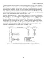
conversions on command. On the assertion of the CONVERT START command, the
sample-and-hold (SHA) is placed in the hold mode, and all the bits of the succes-
sive approximation register (SAR) are
reset to “0” except the MSB which
is set to “1”. The SAR output drives
the internal DAC. If the DAC output
is greater than the analog input, this
bit in the SAR is reset, otherwise it is
left set. The next most significant bit
is then set to “1”. If the DAC output is
greater than the analog input, this bit
in the SAR is reset, otherwise it is left
set. The process is repeated with each
bit in turn. When all the bits have been
set, tested, and reset or not as appropriate, the contents of the SAR correspond to the
value of the analog input, and the conversion is complete.
Figure 4.3.3: Successive approximation ADC.
SHA
DAC
TIMING
CONVERT
START
EOC,
DRDY,
OR BUSY
SUCCESSIVE
APPROXIMATION
REGISTER
(SAR)
OUTPUT
ANALOG
INPUT
COMPARATOR