Conductive Polymers and Plastics in Industrial Applications Part 6 ppt
Bạn đang xem bản rút gọn của tài liệu. Xem và tải ngay bản đầy đủ của tài liệu tại đây (391.59 KB, 20 trang )
solubility.
13,14
The major drawback of such systems is that organic solvents such as dichloro-
methane, m-cresol and N-methylpyrrolidone must be used, which are industrially
undesirable.
Two potential product areas can be explored for large scale electrochemical production
of conducting polymers, these being aqueous colloidal dispersions or water soluble polymers.
A brief description of these polymer technologies is discussed below.
CONDUCTING POLYMER COLLOID PROCESSING
To overcome the water solubility limitations of conducting polymers, aqueous dispersions
that are sterically stabilized
15-21
have been prepared. More recent approaches involve the use
of a core/shell approach where an inner inert colloidal core, such as SiO
2
or TiO
2
, is coated
with the conducting polymer, in the presence of a steric stabilizer, in order to yield uniform
colloid morphology and particle size distributions.
22-25
All of these approaches involve the
production of the conducting polymer component via a chemical oxidative route.
26,27
This
technique involves oxidizing the monomer using a chemical agent and has limitations as dis-
cussed above.
The electrochemical synthesis of conducting polymer colloids is based upon removing
the polymer as it is formed above the electrode surface and stabilizing into colloidal particles
with a polymeric surfactant (i.e., a steric stabilizer). In the early stages of
electropolymerization, the process of oxidation and oligomerization is said to occur within
the diffusion layer above the electrode surface.
28-31
As polymerization continues, the
oligomer solubility (in the electrolyte solution) is exceeded and subsequently precipitates
onto the electrode surface. If the electrolyte flows across the electrode surface fast enough, it
is possible for the polymer to be swept away from the electrode before deposition occurs.
32-34
This process is further facilitated by the presence of the steric stabilizer.
35
The final product is
a colloidal conducting polymer that is doped with the anion of the supporting electrolyte used
during synthesis.
ELECTROCHEMICAL REACTOR DESIGNS
Two electrochemical cells designs were developed “in-house” at IPRI utilizing porous reticu-
lated vitreous carbon (RVC – ERG Aerospace) foam electrodes. RVC is a three dimensional
electrode material with a surface area to volume of 65.6 cm
2
/cm
3
at a porosity of 100 pores
per inch (PPI). RVC was chosen as a replacement for the traditional plate electrode in order to
maximize the electrode surface area and minimize the cell volume. The two designs consid-
ered in this cell development study were either a facing anode/cathode design (Figure 1) or an
sandwiched anode between two opposing cathodes configuration (Figure 2). Each cell com-
partment is separated by an anion exchange membrane (Neosepta
TM
) and protected by insert-
100 Conductive Polymers and Plastics
ing filter paper between the membrane and electrode to minimize fouling. Electrolyte was
flowed from separate catholyte and anolyte reservoirs.
EVALUATION OF ELECTROCHEMICAL REACTORS
In order to establish that the electrochemical cells were operating at optimal efficiency a se-
ries of standardized tests have been developed so that different cells can be compared to one
another. The theoretical and experimental details are discussed below.
The cells were modelled as a Plug Flow Reactor type reactor. Equations exist for the de-
sign and evaluation of each type of reactor.
36
Parameters valid for continuous flow reactors
are based upon the assumption of mass transport limited conditions. The essential equations
for this evaluation process are:
Mass Transfer Coefficient (k
m
)
k
m
=i
L
/zFAC [1]
i
L
limiting current
z number of electrons of reaction
F Faraday constant
A electrode area
Electrohydrodynamic Flow Cell 101
Figure 1. Parallel anode/cathode cell. Figure 2. Sandwiched anode configuration.
C concentration of reactant
In some cases it is preferable to use eq [1] as:
k
m
A=i
L
/zFC [2]
In general, and particularly for cells with plate electrodes, it is possible to use:
k
m
A
S
=i
L
/zFCV
R
[3]
A
S
= A/V
R
V
R
volume of reactor (containing electrode)
For cells with three-dimensional electrodes:
k
m
A
e
=i
L
/zFCV
e
[4]
V
e
electrode volume
Fractional Conversion (X
A
)
X
A
=(C
(in)
-C
(out)
)/C
(in)
or
X
A
=1–(C
(out)
/C
(in)
) [5]
C
(in)
concentration of reactant IN
C
(out)
concentration of reactant OUT
For a PFR operated in single pass mode, and assuming first order mass controlled kinet-
ics, the following relationship will hold:
C
(out)
=C
(in)
exp[-(k
m
A
e
/Q
v
)] [6]
Q
v
volumetric flow rate
X
A
= 1-exp[-(k
m
A
e
)/Q
v
] [7]
102 Conductive Polymers and Plastics
X
A
= 1-exp[-{k
m
A
e
/V
R
}
τ
]
or
ln (C
(out)
/C
(in)
) = -{k
m
A
e
/V
R
}
τ
[8]
τ
residence time (V
R
/Q
V
or V
e
/Q
V
for three dimensional porous electrode)
For a PFR operated in recirculation mode:
X
At
PFR
,
= 1-exp[-(t
X
A
PFR
T
/ τ
] [9]
t time
τ
T
residence time in holding tank
FIGURES OF MERIT
Space-time Yield (
ρ
st
)
ρ
st
= m/V
R
t [10]
m mass of product
In terms of k
m
, at 100% current efficiency,
φ
ρ
st
=k
m
A
e
MC
(in)
[11]
M molecular weight of reactant
Current Efficiency (
φ
)
φ
=Q
p
/Q
T
[12]
Q
p
charge required to produce product
Q
T
total charge used
EXPERIMENTAL
CHEMICALS
Potassium hexacyanoferrate (II) and sodium nitrate were used as supplied from Ajax
(Analar). Milli-Q grade water was used in all experiments.
Electrohydrodynamic Flow Cell 103
EQUIPMENT
A PAR 363 potentiostat/galvanostat was used in all efficiency tests. All potentials were mea-
sured versus a Ag/AgCl reference electrode. A Shimadzu UV-1601 UV-Visible
spectrophotometer was used for all concentration determinations. Data acquisition was made
using a Maclab™ (AD Instruments) interface using Chart V3.3.5 software.
PROCEDURES
Each Cell design was tested by preparinga1Lanolyte solution consisting of 2 mM
K
4
Fe(CN)
6
.3H
2
0
(aq)
and 0.5 M NaN0
3(aq)
.A1Lcatholyte solution of 0.5 M NaNO
3(aq)
. The
anolyte and catholyte solutions were then flowed through their respective compartments at
20, 40 and 60 mL/min by peristaltic pumps. Efficiency tests were carried out at a constant po-
tential of +0.8Vinsingle pass mode.
A chronoamperogram at the applied potential was recorded for both the duration of cell
flushing and sample collection. Initially, 1 to 3 cell volumes were passed through the cell at
+0.8 V, at the flow rate being investigated, and discarded to waste. With the potential still be-
ing applied, a minimum of 1 cell volume was then collected. The collection time (sec) and
actual volume collected (mL) were also determined. The charge passed was then determined
by integrating the area under the curve from the end of the data acquisition and back for the to-
tal collection time (t sec). The concentration of
Fe(CN)
6
3-
produced from
Fe(CH)
6
4-
test
solution was determined by UV-Vis Spectroscopy.
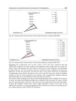
RESULTS AND DISCUSSION
Analysis of the current efficiency
parameters for both cell designs in-
dicated that at + 0.8 V both cells de-
signs had efficiencies of 99 % or
better.
The dependence of the mass
transfer coefficient is shown in Fig-
ure 3. At large residence times, or
low flow rates, the mass transfer
process in the sandwich configura-
tion is slightly higher. At shorter
residence times, higher flow rate,
both cell designs have similar mass
transfer characteristics due to
greater turbulence induced with in
104 Conductive Polymers and Plastics
Figure 3. Effect of sandwich and parallel configuration on the mass
transfer coefficient (K
m
A
e
/V
R
).
the RVC electrodes at higher flow
rates. The effect of this turbulence is
characterized by the rapid increase in
mass transport at lower residence
times (or higher flow rates).
The relationship of space time
yield,
ρ
st
, to residence time, Figure 4,
shows that the sandwich configura-
tion is most efficient at all flow rates
investigated. The sandwich configu-
ration has higher
ρ
st
values due to
minimizing the effect of electrode
shielding and thereby utilizing more
of the available anode surface. In the
sandwich configuration,
ρ
st
decreases
as the electrolyte residence time with
in the cell is also reduced. This is in-
dicative of insufficient electrolyte
contact with the electrode at shorter
residence times, but also shows that
the cell was operating near its optimal
at the lowest flow rate. Increasing the
flow rate from 20 to 60 mL/min re-
duces the space time yield by 15%. In
the case of the parallel configuration,
the space time yield was at a maxi-
mum at shorter residence times. This
result gives further evidence that this
cell design was far less efficient than
the sandwich configuration.
The fractional conversion, Fig-
ure 5, of
Fe(CH)
6
4-
to
Fe(CN)
6
3-
was better than 99% for both cell designs. The sandwich
configuration was again a more efficient cell design. Interestingly, fractional conversion in-
creased with decreasing residence time, or increasing flow rate, due to enhanced electrolyte
turbulence.
Electrohydrodynamic Flow Cell 105
Figure 5. Effect of sandwich and parallel configuration on Fractional
Conversion.
Figure 4. Effect of sandwich and parallel configuration on the space time
yield,
ρ
st
.
EXAMPLES OF POLYMERS SYNTHESIZED USING THESE CELL DESIGNS
A number of conducting polymer colloids have been syn-
thesized using these cell designs. Colloids such as
polypyrrole-nitrate,
2-4
polypyrrole-lactoferrin,
37
polyaniline-polystyrene sulfonate/camphorsulfonic
acid
38
have been successfully synthesized. A TEM, Fig-
ure 6, of a typical polypyrrole nitrate colloid shows typi-
cal colloid morphologies achieved when using these
cells. A major feature of this synthesis technique is that
the colloids formed have a controllable and uniform size
distributions.
CONCLUSIONS
In this paper we have presented a method of
characterizing the efficiency and performance of electro-
chemical flow cells utilizing three-dimensional reticu-
lated vitreous carbon foam electrodes. Cell design
characterization is critical for the successful implementa-
tion and scale up of electrochemical cell, especially with
respect to the scale up from laboratory to prototype and commercial conducting polymer syn-
thesis.
REFERENCES
1 J.N. Barisci, P.C. Innis, L.A.P. Kane-Maguire, I.D. Norris and G.G. Wallace., Synth. Met., 1997, 84, 181-182.
2 J.N. Barisci, C.Y. Kim, D.Y. Kim, J.Y. Kim, J. Mansouri, G.M. Spinks and G.G. Wallace., Colloids and Surfaces A., 1997,
126, 129-135.
3 J. Barisci, J. Mansouri, G. Spinks, G. Wallace, D.Y. Kim and C.Y. Kim, Synth. Met., 1997, 84, 361-362.
4 V. Aboutanos, J.N. Barisci, P.C. Innis and G.G. Wallace., Colloids and Surfaces A., in press.
5 W-P. Hsu, K. Levon, K-S. Ho, A.S. Myerson and T.K. Kwei., Macromolecules, 1993, 26, 318-1323.
6 R.M. McCullough, R.D. Lowe, M. Jayaraman and D.L. Anderson., J. Org. Chem., 1993, 58, 904-912.
7 Y. Wei and J. Tian., Polymer, 1992, 33, 4872-4874.
8 H. Masuda and K. Kaeriyama., Synth. Met., 1992, 13, 461-465.
9 S. Rapi, V. Bocchi and G.P. Gardini., Synth. Met., 1988, 24, 217-221.
10 D. Delabouglise and F. Garnier., New J. of Chem., 1991, 15, 233-234.
11 S-A. Chem and G-W. Hwang., J. Am. Chem. Soc., 1994, 116, 7939-7940.
12 E.E Havinga, W. ten Hoeve, E.W. Meijer, and H. Wynberg., Chem. Mater., 1989, 1, 650-659.
13 Y. Cao, P. Smith and .J. Heeger., Synth. Met., 1992, 48, 91.
14 Y. Cao, P.Smith and A.J. Heeger., App. Phys. Lett., 1992, 60, 2711.
15 H. Eisazadeh, G. Spinks and G.G. Wallace., Mater. Forum, 1992, 16, 341-344.
16 C. DeArmitt and S.P. Armes., Langmuir, 9(1993)652-654.
17 B. Vincent., Polym. Adv. Tech., 1995, 6, 356-361.
106 Conductive Polymers and Plastics
Figure 6. TEM of Polypyrrole-nitrate colloids.
18 M. Aldissi and S.P Armes., Prog. Org. Coatings, 1991, 19, 21-58.
19 H. Eisazadeh, G.Spinks and G.G. Wallace., Mater. Forum, 1993, 17, 241-245.
20 S.Y. Luk, W. Lineton, M. Keane, C. DeArmitt and S.P. Armes., J. Chem. Soc., Faraday Trans., 1995, 91, 905-910.
21 S.P. Armes and B. Vincent., J. Chem. Soc., Faraday Trans., 1987, 228-290.
22 S.P. Armes, S. Gottesfeld, J.G. Beery, F. Garzon, Agnew., Polym., 1991, 32, 2325-2330.
23 R. Flitton , J. Johal, S. Maeda and S.P. Armes., J. of Colloid and Interfacial Sci., 1995, 173, 135- 142.
24 S. Maeda and S.P. Armes., Synth. Met.,1995, 69, 499-500.
25 S. Maeda and S.P. Armes., Chem. Mater., 1995, 7, 171-178.
26 German Patent P 37 29 566.7 Zipperling Kessler & Co.
27 US Patent Application 823416, 823511 and 823512 Allied-Signal, Zipperling Kessler & Co. and Americhem Inc.
28 R. John and G.G. Wallace., J. Electroanal. Chem., 1991, 306, 157.
29 B.R. Scharifker and D.J. Fermin., J. Electroanal. Chem., 1994, 365, 35.
30 B.R. Scharifker, E. Garcia-Pastoriza and W. Marino., J. Electroanal. Chem., 1991, 335, 85.
31 D.E. Raymond and D.J. Harrison., J. Electroanal. Chem., 1993, 355, 115.
32 A.F. Diaz and B.J. Bargon in Handbook of Conducting Polymers, T.A. Skotheim Ed., Vol 1, Marcel Dekker, New York,
1986, 81.
33 C.K. Baker and J.R. Reynolds., J. Electroanal.Chem., 1988, 251, 307.
34 C. Lee, J. Kwak and A.J. Bard., J. Electrochem. Soc., 1989, 136, 3720.
35 H. Eisazadeh, G. Spinks and G.G. Wallace., Mater. Forum, 1992, 16, 341.
36 F. Walsh., “A First Course in Electrochemical Engineering”, The Electrochemical Consultancy, England, 1993.
37 V. Aboutanos, J.N. Barisci, G.R. Harper and G.G. Wallace, submitted ANTEC 98.
38 P.C. Innis, G.Spinks, G.G. Wallace., submitted ANTEC 98.
Electrohydrodynamic Flow Cell 107
Hydroxyethyl Substituted Polyanilines:
Chemistry and Applications as Resists
Maggie A.Z. Hupcey
Dept. of Materials Science and Engineering, Cornell University, Ithaca, NY
Marie Angelopoulos, and Jeffrey D. Gelorme
IBM T.J. Watson Research Center, Yorktown Heights, NY
Christopher K. Ober
Dept. of Materials Science and Engineering, Cornell University, Ithaca, NY
INTRODUCTION
In the field of conducting polymers, solubility of the polymer is a highly desirable quality.
One method that has been widely used to enhance the solubility of conducting polymers is the
incorporation of ring substituents on the polymer backbone.
1-3
However ring substituents
have generally resulted in a decrease in the conductivity of the polymer. Steric constraints im-
posed by the substituents disrupt the coplanarity of the polymer chains as well as increase the
interchain distance. Both factors reduce the mobility of the carriers and as a result lower con-
ductivity is exhibited. In this work, we wish to report a new series of polyaniline copolymers
possessing a hydroxyethyl substituent that improves the solubility of the conducting polymer
and yet retains a high conductivity.
In the field of microlithography, conducting polymers have potentially many uses.
4-6
For
example, it is thought that damage to the gate oxide and to the resist sidewalls during plasma
etching is due to the charging of the insulating resist layer. In SEM metrology of devices and
masks using a conventional insulating resist, charging of the resist yields errors in the mea-
surement, a problem conducting resists have been shown to alleviate.
7
Conducting polymers
have also been proven useful in electron beam (e-beam) lithography, where the exposing radi-
ation is a beam of electrons. Excess electron charge builds up at the surface of an insulating
resist causing severe pattern distortion; with a conducting resist the excess charge is dissi-
pated.
8
With these new hydroxyethyl substituted polyanilines, a simple derivitization to make
a crosslinkable conducting resist is possible.
EXPERIMENTAL
The polyaniline copolymers were synthesized following a well-known procedure.
9
Copoly-
mer compositions were determined via integration on a 300 MHz Varian
1
H NMR. Molecular
weights were measured via GPC eluted with NMP with 0.5% LiCl added to each sample. For
UV-Visible spectra and conductivity measurements, films were spun coat from 5% (wt/wt)
NMP solutions filtered through 5
µ
m filters onto polished quartz discs, then baking the sam-
ples in an 85
o
C oven for 15min. Conductivities were measured via four point probe. Doping
with camphorsulfonic acid (CSA) and acrylamidomethyl-propanesulfonic acid (Aampsa)
was done by adding the dopant in the ratio of 2 mole acid per mole repeat unit to a 5% (wt/wt)
NMP solution of the base polymer, and processed as for the undoped. For HCl doping, the
undoped spun coat films were immersed in 1M HCl overnight and dried under light vacuum.
The methacrylate functionalization was achieved by dissolving the
poly(o-hydroxyethyl)aniline homopolymer in cyclohexanone at 3 wt%, adding
isocyanoethylmethacrylate (IEM) and stirring for 48 hours until complete disappearance of
the isocyanate peak in the IR spectrum.
RESULTS AND DISCUSSION
COPOLYMERIZATION
Seven copolymers were synthe-
sized by varying the molar amount
of o-hydroxyethylaniline mono-
mer in the polymerization (Figure
1). It was found that the incorpo-
rated functionality always ex-
ceeded the feed (Table 1). The
GPC results show that the molecu-
lar weight decreased from a high of
M
n
=22K and leveled off at around
M
n
=12K for feeds larger than 30%.
ELECTRONIC PROPERTIES
In the undoped or base form, the
hydroxyethyl substituted polymers exhibit a red shift in the exciton absorption in the
UV-Visible spectrum as compared to the unsubstituted emeraldine base. A
λ
max
of 609 nm is
observed for the thin film of the unsubstituted polyaniline base whereas a
λ
max
of 629 nm is
observed for the fully substituted poly(o-hydroxyethyl)aniline. The fully substituted
110 Conductive Polymers and Plastics
Figure 1. Poly(o-hydroxyethyl)aniline copolymer synthesis.
poly(o-ethoxy)aniline synthesized and processed in the same way exhibits a dramatic blue
shift to a
λ
max
of 580 nm as compared to emeraldine base and poly(o-hydroxyethyl) aniline.
The ethoxy functionality and the hydroxyethyl substituent basically pose similar geometric
constraints on the polymer. However, the hydroxy functionality provides a means for hydro-
gen bonding between chains thereby reducing the interchain distance. In addition the hydroxy
group provides a means of hydrogen bonding with the processing solvent which may allow
for an expanded chain conformation to be adopted. Previously we have shown a significant
dependence of the exciton absorption on the morphology of the polymer.
10-11
When the copolymers are doped in solution with CSA or Aampsa, the conductivity of
the spun-coat thin films are ~10
-2
Scm
-1
. The hydroxyethyl homopolymer exhibits a conduc-
tivity ~10
0
Scm
-1
, which is of the same order of magnitude as the conductivity of the
unsubstituted polyaniline. The high conductivity exhibited by the poly(o-hydroxyethyl) ani-
line is due to the altered interchain hydrogen bonding as well as improved polymer/solvent
interactions resulting in a more expanded coil conformation. In agreement with this is the
highly delocalized free carrier tail extending into the near-infrared that is observed for the
poly(o-hydroxyethyl)aniline.
LITHOGRAPHY
The presence of the hydroxy substituent also provides a convenient site for further
functionalization of the polymer to provide radiation sensitivity. We have developed a simple
isocyanate-alcohol reaction (Figure 2) in order to add methacrylate functionality without af-
fecting the oxidation state of the backbone. This development is significant because a tradi-
tional Schotten-Baumen esterification with methacrylic acid yields an insoluble mixture of
the desired product along with the HCl doped product. The isocyanate reaction on the other
hand is a reaction that produces no side products. The substituted polymer is produced in so-
lution from which it can be easily spin coated into thin films.
Hydroxyethyl Substituted Polyanilines 111
Table 1. Poly(o-hydroxyethyl)aniline copolymer synthesis data
o-hydroxyethyl aniline
molar feed, %
Actual molar fraction
incorporated, %
M
w
M
n
PDI Conversion
1 2.1 42500 22000 1.93 19.3
10 23 22600 14300 1.59 18.5
20 35 20700 13000 1.59 19.0
30 44 18700 12200 1.54 19.1
50 66 17700 11700 1.51 17.7
100 100 19500 12600 1.55 27.0
This new substituted
polyaniline, PaniIEM, is useful as
a new negative-tone resist. Upon
e-beam and broad band UV light
exposure the methacrylate
crosslinks and becomes insoluble
in the developer. Because of the
improved solubility of the polymer due to the presence of the substituent, the developer can
be a simple polar solvent, in this case ethyl lactate. Figure 3 shows 75 nm lines patterned via
250
µ
C/cm
2
of e-beam radiation at 25KeV accelerating voltage and developed for 1 minute in
ethyl lactate. These patterns are the smallest produced thus far in a single-layer negative tone
conducting e-beam resist. Work is in progress to improve the sensitivity and contrast in order
to reduce the backscatter exposure between the patterned lines.
PaniIEM is also sensitive to broadband UV-Visible light exposure. Further studies to
evaluate the ultimate speed and resolution are underway.
112 Conductive Polymers and Plastics
Figure 3. PaniIEM e-beam exposure: 0.075 µm
equal lines and spaces. Sample: PaniEtOH 100%
methacrylated, CSA doped. Exposure: 250
µC/cm
2
at 25 keV. Develop: 1 min ethyl lactate.
Figure 2. PaniIEM synthesis.
CONCLUSIONS
Poly(o-hydroxyethyl)aniline copolymers have been shown to possess interesting electronic
properties, namely a high conductivity upon doping and a red shift in the UV-visible spec-
trum indicating a high degree of hydrogen bonding between the chains. These new copoly-
mers show considerable promise as resists as they can be derivatized to the radiation sensitive
methacrylate substituted polymer.
ACKNOWLEDGMENTS
The authors would like to thank Jim Bucchignano for assistance with the e-beam exposures
and Nancy LaBianca for helpful discussions. M.H. would also like to thank the SRC
Microlithography program.
REFERENCES
1 Roy, B.C.; Gupta, M.D.; Ray, J.K., Macromolecules, 1995, 28, 1727.
2 Leclerc, M.; D’Arano, G.; Zotti, G., Synth. Met., 1993, 55-57, 1527.
3 Leclerc, M.; Guay, J.; Dao, L.H., Macromolecules, 1989, 22, 649.
4 Lowe, J.; Holdcroft, S., Macromolecules, 1995, 28, 4608.
5 Abdou, M.S.A.; Diaz-Guijada, G.A.; Arroyo, M.I.; Holdcroft, S., Chem. Mater., 1991, 3, 1003.
6 Persson, S.H.M.; Dyreklev, P.; Inganas, O., Adv. Mater., 1996, 8, 405.
7 Angelopoulos, M.; Shaw, J.M.; Lecorre, M A.; Tissier, M., Microelectronic Eng., 1991, 13, 515.
8 Angelopoulos, M.; Patel, N.; Shaw, J.M.; LaBianca, N.C.; Rishton, S.A., J. Vac. Sci. Tech. B, 1993, 11, 2794
9 MacDiarmid, A.G.; Chiang, J.C.; Richter, A.F.; Somasiri, N.L.D.; Epstein, A.J., Conducting Polymers; Alcacer Reidel
Publications: Dordrecht, 1987; pp 105- 120.
10 Seery, T.A.P., Angelopoulos, M., Levon, K., Seghal, A., Synth.Met., 1997, 84, 79.
11 Angelopoulos, M., Dipietro, R., Zheng, W.G., MacDiarmid, A.G., Epstein, A.J., Synth.Met., 1997, 84, 35.
Hydroxyethyl Substituted Polyanilines 113
Electroformation of Polymer Devices and Structures
G. G. Wallace, J. N. Barisci, A. Lawal, D. Ongarato, and A. Partridge
Intelligent Polymer Research Laboratories, University of Wollongong, Australia
INTRODUCTION
The discovery of inherently conducting
polymers (see Table 1) just 17 years ago has
led to the widespread use of polymers in
devices used for sensing, chemical separa-
tions, electromechanical actuators, elec-
tronic components and electrochromics,
amongst many others.
1-4
Not long after the discovery of con-
ducting polymers it was revealed that
simple materials such as polypyrroles,
polythiophenes and polyanilines can be
produced using electrolytic methods, akin
to metal deposition. For example, the
electropolymerization of polypyrrole can
be depicted (rather simplistically) as,
This reaction can also be induced using a chemical oxidant such as FeCl
3
.
Electroformation, however has several advantages.
• A wide range of counterions (A
-
) can be used.
Table 1. Inherently conductive polymers
• The oxidizing strength of the solution can be accurately controlled as a function of
polymerization time. This can be used to control the rate of reaction and to avoid
unwanted side reactions that result in deterioration of the polymer properties.
• Electroformation can be used to obtain spatial control in the assembly of polymer
structures. Patterned electrodes can be addressed with different electroformation
potentials and/or in different feed solutions.
• Electroformation can be used to produce layered structures.
• Electroformation can be used to coat very small surfaces of micro dimensions.
ELECTROFORMATION AT CONVENTIONAL (LARGE) ELECTRODES
As alluded to above the processes involved in
electroformation of conducting polymers are
often oversimplified. Closer examination
5
re-
veals that several steps are involved (Scheme
1).
Once initiated, the reaction proceeds in
solution until sufficient polymer (of high
enough molecular weight) is produced and ex-
ceeds the solubility limit. The polymer
material then precipitates on to the electrode
provided the chemical nature of the surface is
compatible.
Subsequent polymerization is controlled
by a heterogeneous surface (some bare/some
polymer coated) until it is completely cov-
ered. Polymer continues to be deposited
and/or add to reactive oligomers attached to
the electrode surface. Polymers deposited in
this fashion can be removed from the elec-
trode as mechanically stable stand alone
films. They are dense structures with the
chemical and physical properties varying
across the depth of the material. This asym-
metric effect can be enhanced by use of
appropriate structure ordering counterions
such as surfactants. For example, the resultant
116 Conductive Polymers and Plastics
Scheme 1: Electroformation of polypyrrole.
materials can be forced to have hydrophobic properties on one side and hydrophylic proper-
ties on the other.
The use of the electrodeposition process is restricted in that materials of limited dimen-
sions and porosity can be produced. This in turn restricts the use of electroformation to
produce polymer based devices. In addition, in many cases the incorporation of more exotic
counterions to provide molecular functionality often results in a deterioration of mechanical
properties.
ELECTROFORMATION IN HOST POLYMERS
In order to overcome the above limitations, conducting polymers can be grown electrochemi-
cally inside other host structures. This is most readily achieved by simply precoating the elec-
trode substrate with a suitable host polymer (e.g., polyvinyl alcohol). The host material must
be porous enough to allow ingress of solvent, monomer and supporting electrolyte so that the
electropolymerization can proceed. In some instances the host polymer can in fact be used to
provide charge balance, e.g., nafion coatings cast from ethanol can be employed.
A particularly interesting class of host
polymers are hydrogels. For example, we have
utilized crosslinked polyacrylamide with wa-
ter contents greater than 90%. Electrodes may
be cast inside those materials at the time of
gelation. The open porous nature of these ma-
terials makes them ideal for
electropolymerization. It has been found that
the gel networks provides a template for poly-
mer growth the resulting polymer composite
still retaining high (>90%) water content, but
also having electronic conductivity and
electroactivity. These conducting polymer
containing materials can be grown to large di-
mensions with the final shape determined by
that of the gel at the time of gelation.
Spatial distribution of conducting poly-
mers throughout the hydrogel networks is
easily achieved either by dispersing address-
able electrodes throughout the gel or by using
patterned electrode surfaces (Figure 1).
Electroformation of Polymer Devices 117
Figure 1: Schematic representation showing
electroformation of patterned hydrogel-conducting
composite structures.
ELECTROFORMATION OF MICROSTRUCTURES
Electrochemical processes behave differently at micron sized electrodes than at conventional
(large) electrodes. Of particular importance, as far as electropolymerization is concerned, is
the enhanced rate of mass transport of both reactants and products to and from the electrode,
respectively. The former should prevent depletion and hence avoid polymer overoxidation;
the latter, however, prevents deposition.
This means that deposition of
polymers on microelectrodes becomes
more difficult. It is interesting to note
that deposition is not so difficult on line
microelectrodes (10 µm x 1mm). Pre-
sumably the effective concentration at
the longer electrodes increases suffi-
ciently to exceed the solubility limit
before the products are transported
from the electrode.
Nafion precoatings can be used to
advantage in cases where deposition is
difficult in that the ionic nature of the
predeposited material helps attract and
trap the conducting polymer on the mi-
cro surface. The Nafion is precoated by simple evaporation from an ethanol solution (Figure
2).
The effect of the presence of Nafion on the deposition of polypyrroles containing a range
of counterions is shown in Table 2.
Other interesting aspect of micro electrofabrication is that very low currents are encoun-
tered and so polymerization in resistive media can be used. This enables an increased range of
counterions to be incorporated. In fact we have recently shown that this enables
electropolymerization in the gas phase. The cell used is shown in Figure 3.
The micro electrode is precoated with Nafion and pyrrole vapor is present in the en-
closed atmosphere. Imposition of appropriate current densities results in
polymerization/deposition on the micro surface. Cyclic voltammograms recorded in solution
after growth revealed the presence of a conductive electroactive polymer material.
118 Conductive Polymers and Plastics
Figure 2: Schematic representation showing use of Nafion precoatings
to facilitate electroformation on micro structures.
CONCLUSIONS
Advances in the use of electropolymerization enable the use of this approach to produce ma-
terials of varying size and dimension. This in turn will enable the production of a wider range
of polymer based devices and structures.
REFERENCES
1 Adeloju, S.B.; Wallace, G.G., Analyst, 1996, 121, 699-703.
2 Bakhshi, A.K., Bull. Mater. Sci., 1995, 18, 469-495.
3 Gardner, J.W.; Bartlett, P.N., Nanotechnology, 1991, 2, 19-32.
4 Baughman, R.H., 1991, 51, 193-215.
5 John, R.; Wallace, G.G., 1991, 306, 157.
APPENDIX 1
This immobilization of PE also facilitates growth between conducting polymers on insulating
substrates as required for gas sensing systems. In this case polymer must grow laterally be-
tween the four gold tracks to make electrical connection. The resistance of the polymer in the
presence of target volatiles is then monitored by passing a current between the outer tracks
and measuring the potential of the inner tracks. Precoating of polyelectrolyte (Nafion) be-
tween the tracks facilitates this lateral growth.
Electroformation of Polymer Devices 119
Table 2. Electroformation on 10
µ
m elec-
trodes using galvanometric growth
Polymer
Current
density
mA/cm
2
Growth
potential
V
Comment on
polymer
coating
PP/NDSA 2.0 0.49 poor
PP/NDSA/naf 2.0 0.56 good
PP/EBSA 2.0 0.54 extremely poor
PP/EBSA/naf 2.0 0.43 good
PP/BSA 2.0 0.80 extremely poor
PP/BSA/naf 2.0 0.75 good
PP/HBSA 0.2 1.60 extremely poor
PP/HBSA/naf 0.2 0.84 good
PP/4SBA 2.0 0.64 extremely poor
PP/4SBA/naf 2.0 0.60 good
Figure 3: Schematic diagram of gas polymerization cell.
Microelectronic Encapsulation and Related
Technologies: an Overview
Stephen L. Buchwalter
IBM Corporation, Thomas J. Watson Research Center, Yorktown Heights, New York
BACKGROUND
Encapsulation is the term commonly used for device and interconnection protection because
of its long history in electronics, even predating semiconductor devices; and indeed encapsu-
lation by molding plastic around the silicon and a metal leadframe is the predominant form of
device protection in the microelectronic industry on the basis of the sheer volume of packages
manufactured. Encapsulation is a misnomer, however, when it is used as a general term to re-
fer to all forms of device protection, many of which do not entail total enclosure of the device
in plastic or any other single material. In this overview, device protection is used as an abbre-
viation for device and interconnection protection and is meant to be an inclusive term to em-
phasize the common functions of a variety of technologies including, but not limited to
encapsulation.
These common functions fall into two categories—those that are intrinsic to device pro-
tection and those which are extrinsic but closely coupled to device protection. In the first
category there are the important functions of mechanical protection and protection against
corrosion. The microcircuits on silicon devices and connections between the silicon and the
next level of packaging are delicate and, if unprotected, can be damaged by incidental contact
during assembly or actual use. Similarly, the microcircuits and their interconnections must be
protected from environmental effects which can cause rapid failure of the device from corro-
sion of the metallic conductors in the circuitry.
The actual connection of the device to the next level of packaging falls into the extrinsic
category of functions for device protection. This relationship can readily be seen by consider-
ing the molded plastic package as it exists in a variety of forms designed for surface mount
assembly to a printed circuit card. If, for example, because of high stress or high moisture
content, the plastic causes the wirebonds in the package to fail during solder reflow, the mate-
rial has failed its function of providing a package suitable for surface mount assembly. This
function can be seen to directly parallel the function of conductive adhesives as used, for ex-
ample, to attach driver chips to flat panel, active matrix displays. A second extrinsic function
of device protection is heat dissipation. It is readily apparent, for example, that the pathways
offered for heat dissipation by a plastic molded package will be different from those offered
by flipchip on a ceramic module. Recent trends in chip integration have increased require-
ments for both the density of interconnections and heat dissipation. In addition, the
proliferation of semiconductors in mobile computer and communication devices has added
size and weight limitations. These trends towards increased integration and miniaturization
show no signs of abating; and thus, it is clear that the requirements of interconnection and
heat dissipation should be even more tightly integrated into the device protection technology
in order to achieve functional, reliable, compact and cost-effective semiconductor packaging
for the future. For the remainder of this paper, a cursory evaluation of the main device protec-
tion technologies will be given in terms of how well they integrate interconnection and heat
dissipation with device protection and what potential they offer for further improvement in
this regard. Two other inter-related packaging considerations directly impacted by the choice
of device protection are chip test and burn-in and reworkability of the assemblies. These as-
pects will be touched on in this overview as well, including a brief description of one
approach to achieving reworkability without using molded plastic packaging
PLASTIC PACKAGING
Molded plastic encapsulation
1-2
has been the dominant form of device protection, starting
with the dual inline package from the early days of microelectronics. Because of its domi-
nance in packaging the huge volume of memory chips, plastic packaging has had a solid tech-
nology base from which the requirements of more specialized applications have been met by
incremental improvements. Plastic packaging has continued to thrive by increasing the num-
ber of interconnections (I/Os) that can be handled and by reducing the thickness of the pack-
age. The latter has helped overcome some of the thermal limitations of encasing the chip in
epoxy, a poor thermal conductor, as well as meeting requirements for miniaturization. A con-
tinuing attractive feature of plastic packaging is the fact that the packaged chips are easily
handled individually both for test and burn-in to eliminate the chips most likely to fail and for
rework of defective assemblies. An important limitation for the future, however, is the fact
that all plastic packages use wirebonding between pads on the periphery of the chip and a
leadframe. Although the demise of wirebonding has been prematurely predicted before, it
does seem that momentum has shifted to area array interconnection (flipchip attach) because
of its intrinsic advantage for interconnecting high I/O chips. Flipchip is not compatible with
molded plastic encapsulation.
122 Conductive Polymers and Plastics