Modern Developments in X-Ray and Neutron Optics Episode 7 doc
Bạn đang xem bản rút gọn của tài liệu. Xem và tải ngay bản đầy đủ của tài liệu tại đây (2.39 MB, 40 trang )
230 P. Merc`ere et al.
Wave-front measurement Closed loop
X-ray
Hartmann wave-frontsensor
Flat
deflection
mirror
Imaging
optic
Visible CCD
camera
Focal spot imaging
1
2
3
4
Removable
YAG:Ce crystal
Kirkpatrick - Baez
active optic
Command
device
Imaging system
36
36.33
36.63
38.22
Dista
nce (m
)
from the undulator source
38.62
X - ray beam
Visible beam
Hole array
X-ray
CCD camera
Fig. 15.9. Beamline LUCIA end station with the KB active optical system and the
soft X-ray HWS
(b)(a)
Fig. 15.10. Absolute residual wavefront measurements (single CCD image
treatment) (a)beforeand(b) after closed-loop correction
of the photon beam was tuned down to 700 eV to ensure a large illumination
of the sensor with the central Airy disk.
A closed-loop correction was then performed at E =3.64 keV (λ =
0.34 nm), the spatial filter pinhole having been removed. In a single itera-
tion, we succeeded in correcting the phase distortions from 7.7 nm rms and
30.9 nm PV down to 0.8 nm rms and 4.6 nm PV (Fig. 15.10).
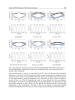
With the KB system correctly aligned, we performed knife-edge scans in
both dimensions to characterize the beam. At the focal spot position, the
beam sections were measured at 2.4 × 2.86 μm
2
FWHM (Fig. 15.11). These
dimensions are close to the theoretical limit given by the source size, the
geometry of the beamline, and the slope errors of the KB mirrors (measured
about 1.1 μrad).
The performance of HWS at these high energies, in particular, the signal-
to-noise ratio and the accuracy of the sensor, is strongly limited by shot noise,
15 Hartmann and Shack–Hartmann Wavefront Sensors 231
Fig. 15.11. Beam knife-edge measurements at the focal spot position after closed-
loop correction with HWS
from the photon-to-electron conversion process in CCDs. The residual wave-
front that can be observed after correction in Fig. 15.10b is, for example, only
the result of shot noise. To overcome this problem, accumulation of several
images is required. The signal-to-noise ratio and the repeatability of wave-
front measurements were studied at 2.1 keV as a function of the number of
images integrated. To achieve a signal-to-noise ratio of about 100, at least 50
CCD images had to be integrated. By integrating 500 CCD images per wave-
front measurement, we improved the repeatability of the sensor to better than
0.04 nm rms. Therefore, high-readout rate CCD cameras may be preferred in
the soft to hard X-ray spectral ranges, when an optimal performance of HWS
is required.
15.4.3 Conclusion
In the EUV spectral range, wavefront measurements were performed over a
wide wavelength range from 7 to 25 nm. The accuracy of the sensor was proved
to be better than λ
EUV
/120 rms (λ
EUV
=13.4 nm), and the sensitivity better
than λ
EUV
/600 rms, demonstrating the high metrological performance of this
system.
In the soft X-ray range, HWS was successfully used to align a 4-actuator
Kirkpatrick–Baez (KB) active optical system. A wavefront closed-loop cor-
rection was performed at E =3.64 keV, which led to beam focusing down to
2.4×2.86 μm
2
FWHM in a single iteration. Variation of the KB focal length is
easily possible by the addition of a curvature term to the closed-loop wavefront
target.
Today, HWS are routinely working between 6 eV (193 nm) and 8 keV
(0.155 nm), with accuracies as good as 0.04 nm rms. The use of high readout
rate CCD cameras for fast accumulation of images and the use of luminescent
screens for a visible Hartmann analysis of the beams, especially for energy
ranges above 10 keV, are currently under investigation. The coupling of HWS
232 P. Merc`ere et al.
with mechanical and bimorph multiactuator deformable mirrors should also
be done in a very near future, to allow easy correction of higher frequency
distortions on synchrotron beamlines.
Acknowledgements
The authors are greatly indebted to “REGION ILE DE FRANCE” for fund-
ing part of the SH-LTP development project. The authors would like to thank
the scientific and technical staffs of ALS beamline 12.0 and SLS beamline
LUCIA (including Markus Janousch) for their support. Finally, the authors
would like to thank several contributors to these works, including Sylvain Bro-
chet, Samuel Bucourt, Gilles Cauchon, Guillaume Dovillaire, Thierry Moreno,
Fran¸cois Polack, Muriel Thomasset, and Philippe Zeitoun.
References
1. W.H. Southwell, J. Opt. Soc. Am. 70, 998 (1980)
2. M. Thomasset, S. Brochet, F. Polack, in Advances in Metrology for X-Ray and
EUV Optics, ed. by L. Assoufid, P. Takacs, J. Taylor. Proc. SPIE, vol. 5921
(2005), p. 12
3. M. Otsubo, K. Okada, J. Tsujiuchi, Opt. Eng. 33, 608 (1994)
4. F. Siewert et al., Third International Workshop on Metrology for X-Ray Optics,
Daegu, Korea, 2006
5. D. Attwood, P.P. Naulleau, K.A. Goldberg, E. Tejnil, C. Chang, R. Beguiristain,
P. Batson, J. Bokor, E.M. Gullikson, M. Koike, H. Medecki, J.H. Underwood,
IEEE Quantum Electron. 35, 709 (1999)
6. K.A. Goldberg, Ph.D. Dissertation, University of California, Berkeley, 1997
7. D. Attwood, Soft X-Rays and Extreme Ultraviolet Radiation – Principles and
Applications (Cambridge University Press, Cambridge, England, 1999)
8. Imagine Optic patent, PCT/FR02/02495, July 2002
9. P. Merc`ere et al., Opt. Lett. 28(17), 1534 (2003)
10. M. Janousch, R. Abela, Th. Schmidt, J.F. van der Veen, R. Wetter, A M. Flank,
P. Lagarde, G. Cauchon, PSI Scientific Report 2002, Volume VII (2002)
11. O. Hignette, G. Rostaing, P. Cloetens, A. Rommeveaux, W. Ludwig, A.K.
Freund, Proc. SPIE, vol. 4499-19 (2001)
12. H.A. Padmore, M.R. Howells, S.C. Irick, T. Renner, R. Sandler, Y M. Koo,
Proc. SPIE, vol. 2856 (1996), p. 145
13. P. Merc`ere et al., Opt. Lett. 31(2), 199 (2006)
16
Extraction of Multilayer Coating Parameters
from X-Ray Reflectivity Data
D. Spiga
Abstract. Detailed analysis of X-ray reflectivity (XRR) angular scans of multilayer
coated samples has been recognized as a powerful tool to investigate their stack
structure. Even though the interpretation of multilayer XRR scans is made com-
plex by the difficulty of managing the large number of parameters that characterize
the stack, computer programs can be used to address the problem of the multi-
parametric fit of experimental XRR scans of multilayers. This chapter describes a
possible strategy to extract the layer thickness values of a multilayer coating from
accurate fitting of XRR scans, based on the Python Program for Multilayers coded.
The results of a best-fit analysis of XRR with transmission electron microscopy data
are also discussed.
16.1 Introduction
The development of multilayer structures intended to enhance the reflection
of radiation with wavelengths in the range of 10–0.01nm, from extreme ultra-
violet to X-rays, and of thermal neutrons, is at present being very actively
pursued. In particular, the use of wideband multilayer coatings is foreseen
in the next generation of soft (E<10 keV) and hard X-ray (E>10 keV)
telescopes with imaging capabilities, like SIMBOL-X [1], Constellation-X [2],
XEUS [3]. The reflection process in multilayers is a complex one, arising from
the interference of the radiation reflected at each interface, beyond the crit-
ical angle for total external reflection. The reflection/focusing performance
over a wide energy band depends essentially on the thickness precision of all
layers and on the smoothness, homogeneity, and sharpness of all interfaces.
It is therefore easy to understand how, in order to improve deposition tech-
niques, methods to investigate the internal structure of multilayer stacks are
needed, and criteria to evaluate the feasibility of the adopted process in terms
of repeatability, uniformity, smoothness, durability must be established.
In this chapter we will compare two techniques that can be used to achieve
a detailed characterization of a multilayer coating: the stack section imag-
ing with TEM (transmission electron microscope) and the analysis of the
234 D. Spiga
XRR (X-ray reflectivity) curves by means of a powerful computer program,
PPM (Pythonic Program for Multilayers), developed by A. Mirone at ESRF
(European Synchrotron Radiation Facility, Grenoble, France). Although the
usefulness of the XRR curves are already recognized as important diagnostic
tools for multilayers, the exact interpretation is made difficult by their com-
plexity and by the large number of parameters characterizing a multilayer.
Therefore, the matching between the experimental and a modeled XRR curve
with manually adjusted parameters can be only qualitative in most cases.
Consequently, the description of the stack structure is often a poorly detailed
approximation of the real one.
On the other hand, the application of PPM to the analysis of XRR data
returns very detailed fits and a realistic description of the multilayer stack. The
advantages of this technique are an effective, quick, nondestructive, in-depth
probing of the distribution of thicknesses throughout the stack.
In the following sections we review some features of X-ray reflection from
multilayers. Then we describe some methods that can be used to extract
information from the XRR curves and apply PPM to the reflectivity data of
a multilayer. Finally, the PPM results are compared with those of TEM and
the difficulties that can arise in such a comparison, due to artifacts in TEM
images, are discussed.
16.2 A Review of X-Ray Multilayer Coatings
Properties
The usefulness of multilayer coatings resides in their capability of reflecting
radiation with wavelength λ in the nanometer/sub-nanometer range when
the incidence angle and the energy exceed the conditions for total external
reflection. The X-ray amplitude reflectivity, r, of a single interface between two
layers with a difference in refractive index, Δn, decays rapidly with increase
in incidence angle ϑ
i
(measured from the surface plane):
r(λ) ≈
Δn(λ)
2sin
2
ϑ
i
. (16.1)
Owing to the very small deviation of the real part of n from unity in X-
rays (δ =10
−4
÷10
−5
, depending on the photon energy and the composition
of the reflecting coating), r is usually very small when the incidence angle is
larger than the critical one. However, if the spacing of the interfaces of layers
in a multilayer is properly conceived, the constructive interference of reflected
rays at each interface enhances the reflectivity at definite photon energies.
The reflectance of a multilayer with 2N layers with thickness t
1
,t
2
, t
2N
and refractive indexes n
1
,n
2
, n
2N
can be computed by recursive applica-
tion of the single-layer reflection formula [4]:
R
m+1
=
r
m,m+1
+ R
m
exp(−iΔφ
m
)
1+r
m,m+1
R
m
exp(−iΔφ
m
)
. (16.2)
16 Extraction of Multilayer Coating Parameters 235
In the last equation, r
m,m+1
is the reflectance of the electric field amplitude
at the mth/(m + 1)th layer interface, Δφ
m
=4πn
m
t
m
sin ϑ
m
/λ is the phase
shift between reflected rays at the mth and the (m + 1)th interface, R
m
is the
amplitude reflectivity of the first m layers. The final X-ray reflectance of the
multilayer is |R
2N+1
|
2
.
The d-spacing d
j
(j =1 N) is the total thickness of the jth couple
of layers (bilayer). Multilayers with constant d-spacing, d
j
= d,aresuited
to reflect narrow bands of the spectrum, whose locations are approximately
(neglecting the beam refraction) determined by Bragg’s law,
2d sin ϑ
i
≈ kλ. (16.3)
In (16.3), k is an integer and λ is the wavelength of the radiation in use.
Multilayers able to reflect a continuous energy band are characterized by a
variable d-spacing throughout the stack (graded multilayers). Radiation with
wavelength λ is reflected when it propagates across bilayers whose d-spacing
satisfies approximately Bragg’s law. A well known possibility is to decrease
gradually the d-spacing according to a power-law [5]:
d(j)=
a
(j + b)
c
. (16.4)
We denote with j =1, 2 N the index of the jth bilayer, ordered from the
multilayer outer surface. Wide-band multilayers of the described type, initially
developed to reflect neutron beams, are called supermirrors and are utilized
also for X-ray mirrors, although in this case the absorption is more severe than
that for neutrons. The coefficients a, b, c,aswellasthenumberofbilayers,N,
and the ratio high-Z material/d-spacing, Γ , have to be optimized in order to
obtain the desired reflectivity as a function of the photon energy. For graded
multilayers Γ can be constant or slowly variable in order to maximize the
reflection efficiency over the energy band to be reflected, i.e., to find the best
trade-off between constructive interference and photoelectric absorption.
As an example, we show in Fig. 16.1 a comparison of the reflectivity as
a function of the photon energy at 0.2
◦
grazing incidence for a constant
d-spacing W/Si multilayer with 200 bilayers, d =8.7nm,Γ=0.46 and
a supermirror with 200 bilayers, a =12nm,b=1.85,c=0.3, and con-
stant Γ =0.46. The supermirror stack was especially designed to provide a
reflectivity as uniform as possible in the energy band 1–70 keV. The reflec-
tivity is improved at low energies by adding a capping layer of tungsten and
a final layer of carbon [6]. Multilayer stacks of the described type [5, 7] are
foreseen for the optics of future hard X-ray imaging telescopes (SIMBOL-X,
Constellation-X, XEUS).
Imperfections of the interfaces, such as microroughness and layers interdif-
fusion, cause a broadening of the interface width. When the two effects can be
236 D. Spiga
Fig. 16.1. Calculated X-ray reflectivity of a constant d-spacing W/Si multilayer
(dashed line) and a W/Si supermirror (solid line) in the energy range 1–70 keV at
the grazing incidence angle 0.2
◦
. The computation supposes zero roughness
considered to be independent of each other, the total interface width, σ,canbe
computed as the quadratic sum of the roughness, σ
r
, and the interdiffusion, σ
d
:
σ
2
= σ
2
r
+ σ
2
d
. (16.5)
One of the effects of interface broadening is the exponential reduction of
the “specular” reflectivity (reflection angle equal to the angle of incidence),
following the N´evot–Croce formula [8]:
R
σ
= R
0
exp
−
16π
2
σ
2
n
h
n
l
sin ϑ
h
sin ϑ
l
λ
2
. (16.6)
In this formula, n
l
,n
h
are the refractive indexes and ϑ
l
,ϑ
h
are the incidence
angles in the two components of the multilayer. The two angles are not equal
due to beam refraction. The reduction is much more severe for high energies
(small λ). The interfacial roughness, σ
r
, has also another effect, the X-ray
Scattering in directions around the specular one. This effect has an important
role in the degradation of imaging quality of X-ray optics.
High precision in the thickness of the layers and a low roughness are
required to ensure a good reflectivity in the energy band of interest. Deviations
of the thickness of the layers from the nominal ones can destroy the ordered
phase shift distribution that generates the high reflectivity or/and the energy
resolution, e.g., for narrow-band multilayers used as monochromators. There-
fore, the reflectivity scan of a multilayer is very sensitive to thickness drifts and
irregularities, and it is easily understood how the deposition facility has to be
carefully calibrated. Furthermore, the deposition rate has to be very steady.
As we shall see in the next section, the sensitivity of X-ray reflectance to
small deviations of the multilayer thickness from the nominal one makes X-ray
reflectivity scans a powerful tool for the investigation of the internal structure
of a multilayer, and consequently, for the evaluation of the improvement of
16 Extraction of Multilayer Coating Parameters 237
a deposition technique. We shall, moreover, see how a detailed description of
the multilayer can be extracted by means of PPM.
16.3 Determination of the Layer Thickness
Distribution in a Multilayer Coating
16.3.1 TEM Section Analysis
A possible technique that can be used to visualize the structure of a multi-
layer coating is the use of a Transmission Electron Microscope (TEM). In TEM
images, the high-density layers appear dark, whereas the low-density layers
are bright. For instance, we show in Fig. 16.2 the TEM sections of a Pt/C
multilayer deposited by e-beam evaporation onto a Si wafer (σ ≈ 0.3 nm) sub-
strate at Media-Lario technologies (Bosisio Parini, Italy); the layered structure
is clearly visible and the thickness of single layers can be directly measured.
For example, the TEM image in Fig. 16.2 highlights the presence of a much
thicker carbon layer due to an instability of the electron beam evaporator.
Indeed, the increase of Pt layers at the right side is an image artifact. It will
be explained in Sect. 16.3.3.
The information provided by the TEM analysis is often useful in helping
to improve the stability of the deposition system. For example, this sample
was a very important test because it constituted the final calibration of the
deposition facility for the manufacturing of a hard X-ray optic prototype [9].
In addition to the layers thickness of the multilayer, TEM images also
provide useful information concerning the crystallization state of the layers,
the interdiffusion between adjacent layers, and sometimes the undulations of
Fig. 16.2. TEM section of a Pt/C multilayer deposited by e-beam evaporation onto
a Si wafer. Pt layers are the dark bands. The section thickness, perpendicular to the
page, decreases from the right to the left side. The growth direction is from bottom
to top (image by L. Lazzarini and C. Ferrari, IMEM-CNR, Parma, Italy)
238 D. Spiga
the interfaces due to the microroughness growth (see Fig. 16.8). This is a
well-known phenomenon, resulting from the combined effect of the replication
of topography of the underlying layers and the random fluctuations of the
deposition process [10].
The TEM images presented in this work are obtained from a JEOL-2000-
FX installed at IMEM-CNR (Parma, Italy). The accuracy in layers thickness
measurements is ∼0.5 nm for multilayers with abrupt interfaces.
16.3.2 X-Ray Reflectivity Analysis
The TEM technique is expensive and the sample preparation is complex and
destructive; therefore, it can be utilized only for selected samples.
However, a large amount of information can be extracted from the analysis
of the X-Ray Reflectivity (XRR) scan of the multilayer. This technique is a
commonly performed test of the reflectance efficiency and consists of prob-
ing the multilayer by means of a thin X-ray beam incident on the coating
and measuring the reflectivity in the specular direction at different incidence
angles.
The usefulness of the XRR measurement as a diagnostic tool is also well
known: the reflectivity as a function of the grazing incidence angle, resulting
from the interference of the radiation reflected at each interface, is usually very
sensitive to the details of the multilayer structure, namely all the values of
thickness, density, and roughness of the layers. For instance, if the multilayer
has a high periodicity and smooth, abrupt surfaces, it will generally exhibit
high, sharp, clearly defined interference peaks (16.3). Conversely, irregularities
of d-spacing will cause the peaks to be “spread” on the angular scale (see
Fig. 16.3), whereas rough or diffuse interfaces will reduce the intensity of
peaks (16.6).
This technique is not destructive, it is quick, and it does not require any
particular preparation of the sample. In addition, the probed surface is usually
large (several cm
2
)evenwithverythinbeamsbecause the measurement is
usually performed in grazing incidence. This reduces selection effects because
local fluctuations of d-spacing are averaged out.
The requirements for XRR measurements for deriving the multilayer
structure are a monochromatic X-ray source with a small divergence (a few
10 arcsec) in order to guarantee a good angular resolution. In addition, the
incident X-ray beam has to be very thin (a few tenth/hundredth microns,
depending on the sample size) in order to be entirely collected by the sample
at very small incidence angles (ϑ
i
> 500 arcsec).
Interpretation of X-Ray Reflectivity Data
Although the analysis of XRR curves is a widespread tool, their exact inter-
pretation is a complex problem. Because of the sensitive dependence of
XRR measurements on the thickness, density, roughness of all layers, the
16 Extraction of Multilayer Coating Parameters 239
Fig. 16.3. Comparison of the measured X-ray reflectivity scans of two Ni/C multi-
layers with the same average value (9 nm), but different dispersion of the d-spacing
(deposited in 2003 by e-beam evaporation at Media-Lario technologies). The smaller
dispersion in the case of the solid line curve is made apparent by the narrower and
more regular peaks. The approximate Γ factor is 0.2 for the solid line and 0.4 for
the dashed line
Fig. 16.4. Experimental X-ray reflectivity of the W/Si multilayer with 30 bilayers
deposited by e-beam with ion assistance (grey dots). The black solid line is the initial
reflectivity model, computed with the IMD package [11], assuming a multilayer with
constant d-spacing
interpretation of XRR scans is not trivial. The XRR of a multilayer with
N bilayers can be computed by applying recursively (16.2) including (16.6)
to account for the roughness/interdiffusion. However, to fit the reflectance
modeling to the experimental dataset it would be necessary to handle 4N
parameters, namely all the thickness and roughness values of all layers,
assuming at least constant density values throughout the stack.
We show in Fig. 16.4 an example we adopt in the following pages:
the experimental XRR scan at 8.05 keV (measured at INAF/Osservatorio
240 D. Spiga
Astronomico di Brera) of a W/Si multilayer (30 bilayers). The sample was
deposited in 2004 by e-beam evaporation with Ar+ ion etching onto a Si
wafer (σ ≈ 0.3nm) at Media-Lario technologies. The deposition was the first
test of the ion-etching facility: this test confirmed that the ion beam is effective
in reducing the roughness of a W/Si multilayer, as proven by AFM measure-
ments. The XRR scan was measured with a BEDE-D1 X-ray diffractometer
with a Cu-anode X-ray tube as source. The Cu Kα X-ray line is filtered by a
Si Channel-Cut crystal and collimated by a system of slits, obtaining a thin
(70 μm wide, 25 arcsec divergent) and monochromatic (ΔE/E ≈ 10
−4
)X-ray
beam. The reflected beam is collected by a photon counter, a scintillator with
high linearity.
The measured XRR curve (dots) exhibits a complex structure with broad
peaks: the solid curve in Fig. 16.4 is the best fit that could be reached using
a constant d-spacing model with d =5.3nm,Γ=0.43, and σ =0.5nm. The
density values were assumed to be 18.1g cm
−3
for W and 1.8g cm
−3
for Si,
lower than the natural ones (19.3g cm
−3
for W and 2.3g cm
−3
for Si), in
agreement with previous single-layer calibrations. However, the disagreement
is apparent. Therefore, the multilayer has a variation of d-spacing in the stack:
it is likely to be ascribed to a variation of the evaporation rate, combined with
fluctuations of the etching rate in the ion-etching facility. However, the exact
determination by means of manual fits of the trend of thickness of layers is
very difficult.
Fitting Algorithms
The problem of extracting the stack parameters from an XRR scan can be
solved by means of numerical codes, which are able to explore a very wide
range of parameters in order to find the best solution. The first step is the
assumption of an appropriate model for the multilayer stack, as defined by a
set of independent parameters. For example, one can assume a continuous drift
or an irregular variation of the thickness and roughness of the layers. In the
first case the free parameters are the coefficients of the function describing the
drift. In the second, each thickness value is a free parameter. Alternatively,
the model may consist of a drift superimposed onto a fluctuating term.
The second step is the choice of a figure of merit (FOM) to measure the
closeness of the experimental curve to the computed one using a standard
method with variable parameter values. The problem of searching for the best
fit is therefore reduced to the minimization of the FOM, and the best solution
is the set of values for parameters corresponding to the global minimum of the
FOM. A possibility for the FOM could be the χ
2
of the measured-simulated
data. However, since in a reflectivity minimum the X-ray beam probes a much
larger depth of the stack, we can recover more information concerning the
thickness of the deepest layers in reflection minima than at reflectivity peaks,
even though the reflectivity signal is usually very weak. The FOM should
then be calculated from the logarithm of the reflectivity in order to make the
16 Extraction of Multilayer Coating Parameters 241
algorithm sensitive to the XRR features located near the reflection minima.
A possible FOM fulfilling this requirement is
FOM =
i
(log R
m
(i) − log R
c
(i))
2
. (16.7)
Here R
m
(i)andR
c
(i) are the measured and calculated reflectivity at the ith
angular position of the X-ray mirror. Another possibility is
FOM =
i
|log R
m
(i) − log R
c
(i)|. (16.8)
These and other FOMs have been adopted in the literature (see [12] for a
detailed discussion).
Several algorithms have been studied in the past years aimed at FOM
minimization working on a large number, F, of parameters:
• Downhill simplex. Starting from an initial guess for the parameters values,
asetofF +1 point (the simplex) makes a series of moves selecting the val-
ues with the smallest value of the FOM [13]. This method converges to the
nearest local minimum, where it gets trapped. A more global minimum can
be found by iterating this procedure from different initial guessed values
and selecting the best result. The method is then called Iterated Simplex:
this method has been utilized for the optimization of X-ray multilayers for
the optics of XEUS [14].
• Levenberg–Marquardt (LM). Starting from guessed values, the FOM min-
imum is searched through a combination of inversions of the Jacobian
matrix of R
c
with respect to the parameter set [15, 16]. This method
works better when initial values lie near the global minimum, e.g., the
initial values can be computed analytically from the experimental reflec-
tivity curve [17]. The LM can be utilized to refine the calculated parameter
values [18].
• Genetic Algorithms (GA). This very powerful class of minimization algo-
rithms has been used by several authors (see e.g. [12, 19, 20]) in facing
the problem of fitting the reflectivity of multilayers. This method gener-
ates a large number of sets of parameter values, called individuals,and
simulates the evolution of the population through random mutation and
exchange of subsets of parameter values between individuals. The pop-
ulation is also subjected to a “Darwinian” selection in that the poorer
performing individuals are suppressed. The survivors generate the next
generation of individuals. The evolution of the population should lead to
the best fit after a sufficiently large number of generations.
• Downhill Annealing. This method combines the local minimization of the
Downhill Simplex with the capability of the “Simulated Annealing” to
escape from local minima [21–23]. The convergence of the Simplex to the
nearest local minimum is compared with the thermalization process at
a “temperature” T . Each movement of the simplex is compared with an
242 D. Spiga
energetic transition governed by Boltzmann statistics, with the FOM play-
ing the role of the energy. Owing to the tendency of physical systems to
reach the minimum energy, the Simplex will preferably move down the
FOM gradient. However, transitions that increase the FOM are also sta-
tistically possible. Initially T is high, and so is the rate of transitions
that increase the FOM. In this phase the program has a high capability of
escaping from local minima. When T is slowly decreased (the “annealing”),
the likelihood of occurrence of transitions that increase the FOM becomes
smaller and smaller, and the system approaches the global minimum. This
algorithm has already been implemented in a program developed at ESRF
for multilayer stack analysis [24].
PPM (Pythonic Program for Multilayers)
The program we adopted to perform the XRR fit of the reflectivity curve is
PPM (Pythonic Program for Multilayers), developed by A. Mirone (ESRF).
PPM can perform detailed fits of XRR curves at one or more photon energies
at the same time. PPM takes as input an XML file that describes the modeling
of the stack (thickness drift, free variation of each layer, increasing roughness,
etc.) with values initially set by the user. The parameters can vary within fixed
limits, also set by the user. The comparison of the calculated XRR curve(s)
with the measured one(s) is made quantitative by evaluating the FOM, where
(16.8) was adopted. PPM then searches recursively the global minimum of
the FOM by means of the Downhill Annealing algorithm.
The fitting capabilities of PPM were used to perform fits of U/Fe multi-
layers in order to measure the optical constants of uranium [25]. Moreover, in
a previous SPIE volume [26] we utilized PPM to analyze some XRR curves of
X-ray multilayers, which yielded very accurate fits and a detailed description
of the coatings. In that work we also compared the results obtained from the
PPM analysis with TEM images of sections of the same samples, finding a
good agreement within the error of TEM. In this work we will apply PPM to
another example.
16.3.3 Stack Structure Investigation by Means of PPM
Application of PPM to the XRR Curve of a Multilayer
The analysis with PPM has been applied to the XRR curve at 8.05 keV in
Fig. 16.4 in order to derive the internal structure of the stack. PPM was run
in a LINUX environment with an AMD Sempron64 3400 processor (2 GHz).
Initially, we assumed a second-order drift of W and Si, and the two trends were
considered to be independent. The density values were known from previous X-
ray measurements on single layer samples obtained with the same deposition
facility: 18.1g cm
−3
for W and 1.8g cm
−3
for Si (see Sect. 16.3.2). The rms
16 Extraction of Multilayer Coating Parameters 243
Fig. 16.5. The analysis performed via PPM on the XRR scan of the W/Si multi-
layer, assuming independent, second-order polynomial drifts of thickness values of
W and Si, and a quadratic drift of the roughness
roughness was also assumed to drift throughout the stack with a second-
order polynomial trend. No difference between the roughness of the W and
Si layers was assumed. PPM was then run on the experimental data after the
subtraction of the instrumental noise and the smoothing of apparent noisy
features in the reflection minima.
The fit was performed starting from values obtained from the parameters
adjusted manually (Fig. 16.4), and the final achieved fit is shown in Fig. 16.5.
The shape of the peaks is now fitted better, but not perfectly in particular at
the smallest incidence angles. The fitting procedure required just 10 min.
The imperfections in the fit should be ascribed to the assumed continuous
drift, which cannot simulate all the irregularities of the d-spacing. There-
fore, the fit has been repeated by letting all the layer thicknesses to vary
freely within 1 nm, starting again from the values inferred from the man-
ual fit (2.3 nm for W, 3.0 nm for Si). Only the first deposited Si layer was not
included in the model because its presence does not noticeably affect the XRR
diagram. The roughness is still assumed to have a second degree polynomial
drift, and the density values are still the same as used in the previous step.
However, because of the huge increase in the number of free parameters, the
fitting procedure needed to be restarted several times, with changes in the
limits of the allowed values when the fitting value came too close to one of
them. The computation required 2 h, but the experimental XRR curve is now
fitted accurately (see Fig. 16.6).
The fit results are summarized in Fig. 16.7, where the distribution of thick-
nesses of W and Si layers is plotted as a function of their bilayer index,
numbered from the substrate. The thickness of Si layers oscillates around
the 3.0 nm value and that of W around 2.3 nm. Moreover, the rms roughness
exhibits an apparent, almost linear increase from 0.31 to 0.55nm, going from
244 D. Spiga
Fig. 16.6. The XRR curve fit with PPM by letting each layer thickness value vary
freely
Fig. 16.7. The W/Si multilayer stack structure derived by PPM
the substrate to the multilayer outer surface. This increasing evolution of the
roughness is expected classically, even if the use of the ion etching device
contributed to restrict the roughness growth.
In the next section we shall compare the analysis results with those of the
TEM image (Fig. 16.8).
Interpretation of TEM Images and Comparison with PPM
The results of the fit in Fig. 16.7 can be cross-checked with the results of the
sample section taken with TEM (Fig. 16.8). From the image we can see directly
the microroughness growth detected by the PPM analysis: undulations with
∼25 nm period with increasing amplitude in the growth direction. From a
profile of the TEM image the thickness values were extracted, except for the
16 Extraction of Multilayer Coating Parameters 245
Fig. 16.8. TEM image of the section of the W/Si multilayer sample deposited
by e-beam evaporation with ion etching (at Media-Lario technologies). The growth
direction is from bottom to top (image by L. Lazzarini and C. Ferrari, IMEM-CNR)
bilayers 10 and 11, and the comparison of PPM results with those of TEM is
shown in Fig. 16.9.
When directly compared, the two distributions of layers as derived using
the two methods would be at first glance in disagreement. On the average,
the W layer thickness values measured with TEM are larger than the values
inferred by PPM by 0.5 nm, whereas the contrary occurs for Si layers.
However, as anticipated in Sect. 16.3.1, the thickness values can be altered
by image artifacts: the roughness of the high-Z element tends to obscure the
low-Z element layers by superposition of rough profiles on the image plane.
Thus, the W layers in Fig. 16.8 appear thicker, and the Si layers appear thinner
than they actually are. This is more clearly seen in Fig. 16.2 with the Pt/C
multilayer sample, where the obscuring of the C layers increases rapidly with
the thickness of the TEM section up to the point of disappearing completely
on the right side of the image.
In fact, this artifact depends on the TEM section thickness. When the
TEM sample is thin, a small number of profiles overlap in the image plane
and the measured thickness values are a good approximation to real ones, i.e.,
the distance between the average levels of the interfaces. In Fig. 16.2, this
246 D. Spiga
Fig. 16.9. The thickness distribution in W/Si multilayer as computed by PPM
(marks) compared with TEM findings (lines). The error bars are the uncertainties
of the TEM measurement
occurs near the edge of the sample, where the section is very thin. Far from
the edge, a very large number of rough profiles are integrated with random
phases along the line of sight, which is perpendicular to the page. This is
schematically depicted in Fig. 16.10. Note that the obscuration equals roughly
twice the maximum amplitude of the high-Z layers. Since the X-ray reflection
occurs at the average level of the interfaces (the dashed lines in Fig. 16.10),
the measured values by PPM will differ from those measured with TEM by
the apparent “broadening” of dark layers.
TEM Artifacts Correction: Comparison of d-Spacings
To estimate quantitatively the correction of TEM data, we can suppose the
interfaces to be isotropic. Therefore, the roughness PSD P (f)alongthe
16 Extraction of Multilayer Coating Parameters 247
Fig. 16.10. Artifacts in TEM images of multilayers. If the TEM section is thin
(left) the projection of the high-Z material layers approximately equals the average
thickness (delimited by the dashed lines). If the thickness of the section is increased
(center) the low-Z layers will start being “shaded” by the irregularities of the high-Z
layers. Thus, the measured thickness with TEM (vertical arrows) will be lower and
lower (right)
line-of-sight (perpendicular to the page) approximately equals the measured
one in the TEM image plane (parallel to the page), and for a given thickness
of the TEM section τ we can compute the broadening Δz of dark layers as
twice the peak value of the roughness:
Δz ≈ 2
√
2
+∞
1/2τ
P (f)df
1/2
. (16.9)
In (16.9) the factor
√
2 is the peak to rms ratio. The root of the integral
of the PSD is the rms roughness and 1/2τ is the minimum frequency being
integrated, in other words, the minimum frequency with a maximum of the
oscillation in a length τ. The increase of Δz with τ is partly due to the
enlargement of the frequency band and partly due to the rapid increase of
P (f) for decreasing frequencies. Furthermore, τ in the TEM section is not
constant, but it is larger in the upper part of the image. This makes the
evaluation of Δz quite difficult.
Some constraints can be set on the value of τ by noting that we do observe
profile undulations in the upper part of the TEM image (see Fig. 16.8). Then,
under the reasonable assumption that the surface topography is isotropic, τ
should be of the order of the average period of the observed oscillations (some
20 nm). The P (f) function was not measured at such a short spatial scale;
hence, we cannot compute directly Δz. We can, however, at least state that the
root of the integral in (16.9) should be much less than the σ roughness value
inferred from the XRR analysis, which usually refers to all the spatial periods
below some microns. Such a value for σ could be used if the TEM sample
were much thicker, i.e., τ ≈ 1 μm, and the correction Δz would amount (on
average) to 2
√
2 ×0.4nm ≈ 1.1 nm. Conversely, if the TEM sample is much
thinner than 1 μm, Δz<1.1nm.
In fact, if we assume Δz =0.5 nm, the main discrepancy between TEM
data and PPM findings is eliminated. To account for the projection effect
248 D. Spiga
Fig. 16.11. Comparison of d-spacings as extracted from the XRR curve (marks)
and TEM (lines + bars). The agreement is satisfactory
mentioned, this amount has to be subtracted from W thickness values as
measured from TEM and to be added to the Si layers. The residual discrep-
ancies can be due to errors in localization of the interfaces in the TEM image.
The evolution of the roughness and the increase of τ can be the cause of the
larger discrepancy in the last bilayers.
A confirmation of the assumed interpretation comes from the comparison
of bilayer d-spacings obtained by XRR and TEM. They should not be affected
by the projection effect in TEM image because the correction for W and Si
have opposite signs and cancel out. The d-spacings comparison is shown in
Fig. 16.11. Almost all the d-spacings, as measured with PPM, are in agreement
with TEM to within the TEM error bars (0.5 nm). This is a confirmation of
the correctness of the analysis performed with PPM.
16.3.4 Fitting a Multilayer with Several Free Parameters
We also applied PPM to fit the XRR curve of a graded multilayer deposited
by DC magnetron sputtering at the Harvard-Smithsonian Center for Astro-
physics (Boston, USA), using a deposition facility suitable for the production
of multilayer coated hard and soft X-ray mirror shells [27]. The substrate
used was a superpolished fused silica sample (σ ∼ 0.1 nm). The multilayer
is described by two power-law distributions of d-spacings: the outermost 20
bilayers are thicker and reflect soft X-rays, the innermost 75 bilayers are
thinner and reflect the hardest X-rays.
The reflectivity of the sample was measured using the BEDE-D1 diffrac-
tometer at INAF/Osservatorio Astronomico di Brera up to 15,000 arcsec
grazing incidence at the photon energy of 8.05 keV. In this case, because of
the very large number of bilayers, we could not take all the thickness value as
free parameters. To get around this, we initially modeled the thickness trends
16 Extraction of Multilayer Coating Parameters 249
Fig. 16.12. PPM fit of a graded W/Si multilayer deposited at the Harvard-
Smithsonian Center for Astrophysics.Measureddata(dots) and PPM fit (line)
following two power laws, assuming as free parameters a, b, c, as in (16.4). To
account for a drift of the Γ factor (see Sect. 16.2) throughout the stack, we
assumed that the trend of the parameters for W and Si trend were indepen-
dent. The roughness was free to drift according to second-order polynomial
trends, one for each stack. The search for the best fit with PPM enabled us
to determine the parameters a, b, c, for the two stacks.
In a second step, to refine the fit, the layers thickness values were treated as
free variables, starting with the values found in the previous step and allowing
small variations in them (±0.3 nm). The very detailed fit results are shown in
Fig. 16.12.
16.4 Conclusions
The methodology described here highlights the potential of the XRR scan
analysis for investigations of the internal structure of nearly periodic and
graded multilayers. The problem of multi-parametric XRR curve fitting can be
solved by means of computer codes based on several algorithms. In particular,
PPM has proven to be very effective in fitting structured XRR curves, and the
structure inferred is in good agreement with TEM results after the correction
of TEM artifacts.
XRR analysis with PPM yields a reliable description of the multilayer
structure, on condition that the experimental curves are fitted very accurately.
To do this, the fitting strategies can be summarized as follows:
1. For multilayers with 30 bilayers or less, assume each layer thickness value to
be a free variable. Then let them vary within a wide variability range (1 ÷
2 nm) in order to explore a wide parameter space region. If the multilayer
250 D. Spiga
has a nearly constant d-spacing, assume a constant thickness throughout
the stack as an initial guess.
2. For multilayers with more than 30 bilayers, start the fit by first assuming
a continuous thickness drift in the stack. Then, let all layers vary freely
within small (0.4 nm) limits around the values found in the previous step
of the fit procedure. The fit can be restarted several times, adjusting the
limits each time, until a satisfactory fit is reached.
3. If the experimental curve exhibits high reflectivity peaks, a preliminary
computation can be done, assigning weights to data proportional to the
reflectance values in order to approximately fit the primary reflectance
peaks. The parameters should then be refined in a successive PPM run
without weights.
4. If the actual density values are uncertain, they can be assumed as fit
variables within small limits.
5. The roughness values can be considered as constant throughout the stack
only for multilayers with less than 20 bilayers, otherwise a drift of the
roughness should be included.
6. Possible angular offsets in the experimental curves, instrumental noise, and
the angular resolution of the measurement should be accurately evaluated
and included in the calculations.
Finally, when comparing XRR analysis and TEM results, correct the thick-
ness values obtained from TEM according to (16.9). These fitting methodolo-
gies were tested on several multilayer samples [26] in addition to the example
provided in the present work.
Further tests are foreseen in order to establish the reliability of PPM as a
diagnostic tool for multilayers. If confirmed, the systematic use of the XRR
scan analysis with PPM will be an important diagnostic tool in the devel-
opment of multilayer mirrors for several applications, such as the wideband
reflective coating of future soft and hard X-ray telescopes.
Acknowledgments
The author gratefully acknowledges A. Mirone, C. Ferrero, M. Sanchez del Rio
(European Synchrotron Radiation Facility, Grenoble, France) for the develop-
ment of the program PPM, L. Lazzarini and C. Ferrari (IMEM-CNR,Parma,
Italy) for the TEM analysis of the samples and G. Nocerino (Media-Lario
technologies, Bosisio Parini, Italy) for the support to this work. The valu-
able collaboration of G. Valsecchi, G. Grisoni, M. Cassanelli (Media-Lario
technologies) is kindly acknowledged.
The author also thanks G. Pareschi, D. Vernani, V. Cotroneo, R. Canes-
trari (INAF/Osservatorio Astronomico di Brera) for support and useful
suggestions and S. Romaine, P. Gorenstein, R. Bruni (Harvard-Smithsonian
CfA, Boston, USA) for providing us with the graded multilayer sample referred
to in Fig. 16.12. The graded multilayer reported in Fig. 16.1 was designed by
V. Cotroneo (INAF/Osservatorio Astronomico di Brera).
16 Extraction of Multilayer Coating Parameters 251
The author is indebted with MIUR (the Italian Ministry for Universities)
for the COFIN grant that provided support for the development of multilayer
coatings for X-ray telescopes, and the European Science Foundation – COST
cooperation, action P7 for the grant that made the PPM training at the ESRF
possible.
PPM is open-source software; it can be freely downloaded from ftp://www.
esrf.fr/pub/scisoft/ESRF
sw/linux i386 03/.
For PPM installation support, please contact the author of the present
chapter.
References
1. G. Pareschi, P. Ferrando, Exp. Astron. 20, 139 (2006)
2. P. Gorenstein, A. Ivan, R.J. Bruni, S.E. Romaine, F. Mazzoleni, G. Pareschi,
M. Ghigo, O. Citterio, SPIE Proc. 4138, 10 (2000)
3. A. Parmar, M. Arnaud, X. Barcons, J.M. Bleeker, G. Hasinger, H. Inoue,
P. Palumbo, M.J. Turner, SPIE Proc. 5488, 388 (2004)
4. L.G. Parrat, Phys. Rev. 95(2), 359 (1954)
5. K.D. Joensen, P. Voutov, A. Szentgyorgyi, J. Roll, P. Gorenstein, P. Høghøj,
F.E. Christensen, Appl. Opt. 34(34), 7934 (1995)
6. G. Pareschi, V. Cotroneo, D. Spiga, M. Barbera, M.A. Artale, A. Collura,
S. Varisco, G. Grisoni, G. Valsecchi, SPIE Proc. 5488, 481 (2004)
7. Y. Tawara, K. Yamashita, H. Kunieda, K. Tamura, A. Furuzawa, K. Haga,
N. Nakajo, T. Okajima, H. Takata, et al., SPIE Proc. 3444, 569 (1998)
8. L. N´evot,P.Croce,RevuePhys.Appl.15, 761 (1980)
9. G. Pareschi, O. Citterio, S. Basso, M. Ghigo, F. Mazzoleni, D. Spiga, W. Burk-
ert, M. Freyberg, G.D. Hartner, G. Conti, E. Mattaini, G. Grisoni, G. Valsecchi,
B. Negri, G. Parodi, S. Marzorati, P. Dell’Acqua, SPIE Proc. 5900, 47 (2005)
10. D.G. Stearns, Appl. Opt. Lett. 62(1515), 1745 (1993)
11. D.L. Windt, Comput. Phys. 12, 360 (1998)
12. M. Wormington, C. Panaccione, K.M. Matney, D.K. Bowen, Phil. Trans. R.
Soc. London 357, 2827 (1999)
13. J.A. Nelder, R. Mead, Comput. J. 7(4), 308 (1965)
14. V. Cotroneo, G. Pareschi, SPIE Proc. 5536, 49 (2004)
15. K. Levenberg, Quart. Appl. Math. 2, 164 (1944)
16. D. Marquardt, SIAM J. Appl. Math. 11, 431 (1963)
17. I.V. Kozhevnikov, I.N. Bukreeva, E. Ziegler, NIM-A 460, 424 (2001)
18. E. Ziegler, C. Morawe, I.V. Kozhevnikov, T. Bigault, C. Ferrero, A. Tallandier,
SPIE Proc. 4782, 169 (2002)
19. M. Sanchez del Rio, G. Pareschi, SPIE Proc. 4145, 88 (2001)
20. D.
ˇ
Simek, D. Rafaja, J. Kub, Mat. Struct. Krystalografick´aspoleˇcnost 8(1),
16 (2001)
21. N.A. Metropolis, A.W. Rosenbluth, M.N. Rosenbluth, A. Teller, E. Teller,
J. Chem. Phys. 21(6), 1087 (1953)
22. V. Cerny, in Comenius University Report (Bratislava, Slovakia, 1982)
23. S. Kirkpatrick, C.D. Gelatt, M.P. Vecchi, Science 220, 671 (1983)
252 D. Spiga
24. E. Ziegler, C. Ferrero, F. Lamy, C. Chapron, C. Morawe, CPDS 2002 45,
45 (2002)
25. S.D. Brown, L. Bouchenoire, A. Mirone, V. Cotroneo, in Progress Report ESRF
(Grenoble, France, 2004)
26. D. Spiga, A. Mirone, G. Pareschi, R. Canestrari, V. Cotroneo, C. Ferrari,
C. Ferrero, L. Lazzarini, D. Vernani, SPIE Proc. 6266, 346 (2006)
27. S. Romaine, S. Basso, R. Bruni, W. Burkert, O. Citterio, G. Conti,
D. Engelhaupt, M. Freyberg, M. Ghigo, P. Gorenstein, M. Gubarev, G.D. Hart-
ner, F. Mazzoleni, S. O’Dell, G. Pareschi, B. Ramsey, C. Speegle, D. Spiga,
SPIE Proc. 5900, 225 (2005)
17
Hard X-Ray Microoptics
A. Snigirev and I. Snigireva
Abstract. This chapter presents a summary of micro-focusing optics and methods
for X-rays in the energy range 4–100 keV, as provided by synchrotron radiation
sources. The advent of third generation storage rings such as the ESRF, the APS and
Spring-8 with X-ray beams of high brilliance, low divergence and high coherence has
made possible efficient X-ray focusing and imaging. The main emphasis is on those
methods which aim to produce submicrometre and nanometre spatial resolutions
in imaging applications. These methods fall into three broad categories: reflective,
refractive and diffractive optics. The basic principles and recent achievements are
discussed for optical devices in each of these categories.
17.1 Introduction
A summary of microfocusing optics and methods for hard X-rays is pre-
sented. The hard X-ray region is taken as extending from about several keV
(∼4 keV) to gamma rays with several hundreds keV (∼100 keV) provided by
synchrotron radiation sources. The advent of third generation storage rings
like ESRF, APS, and SPring-8 with radiation beams of high brilliance, low
divergence, and high coherence makes possible efficient X-ray focusing and
imaging. X-ray microscopy techniques are presented first. The main emphasis
will be put on those methods that aim to produce nanometer resolution. These
methods fall into three broad categories: reflective, refractive, and diffractive
optics. The basic principles and recent achievements will be discussed for all
optical devices. The report covers the latest status of reflective optics, includ-
ing mirrors and multilayers, capillaries and waveguides. Special attention will
be given for successful development of Kirkpatrick–Baez (KB) systems pro-
viding nanometer focusing in two dimensions. The basic principles and the
state of the art of diffractive optics such as Fresnel zone plates are reviewed.
Improvement of the spatial resolution without loss of efficiency is difficult
and incremental due to the fabrication challenges posed by the combination
of small outermost zone width and high aspect ratios. Particular attention
will be given to recent invention of refractive optics. Refractive optics is a
256 A. Snigirev and I. Snigireva
rapidly emerging option for focusing high energy synchrotron radiation from
micrometer to nanometer dimensions. These devices are simple to align, offer
a good working distance between the optics and the sample, and are expected
to become standard elements in synchrotron beamlines instrumentation in
general and in high energy X-ray microscopy in particular.
17.2 X-Ray Microscopy
The history of X-ray microscopy goes back to 1896, the year following the
discovery of X-rays by Roentgen. The method used to study the struc-
tural details of biological objects by enlargement of X-ray radiographs was
called by P. Goby as microradiography in 1913 [1]. Beginning in the late
1940s, X-ray microscopy with grazing incidence mirror optics was proposed
by P. Kirkpatrick in order to surpass the optical microscope in resolution [2].
As a branch of earlier developments in electron microscopy, projection
microscopy was proposed by Cosslett and Nixon [3] and it became very popu-
lar since the 1950s. In the early 1970s, several groups started new technological
developments of X-ray optics, in particular, Fresnel zone plates, and the mod-
ern era of X-ray microscopy started. In 1974, Schmahl and collaborators
built a full-field transmission microscope at DESY (Deutsches Elektronen
Synchrotron) in Germany [4]. Kirz and Rarback at NSLS (National Syn-
chrotron Light Source) at Brookhaven National Laboratory in USA built
the first scanning transmission microscope using a zone plate objective in
1982 [5]. Traditionally, this type of X-ray microscopy deals with rather soft
X-ray energies (100–2,000eV), in particular, in the so-called water window
region between the K-shell X-ray absorption edges of carbon and oxygen at
4.4 and 2.3 nm, where organic materials show strong absorption and phase
contrast while water is relatively nonabsorbing. This enables imaging of spec-
imens up to ∼10 μm thickness, with high intrinsic contrast using X-rays with
a lateral resolution down to 15 nm [6].
In recent years, considerable progress has been made in X-ray microscopy
in the hard X-ray regime (E>4 keV), as a result of the development of high
brilliance, high energy X-ray sources coupled with advances in manufactur-
ing technologies of focusing optics. One of the key strengths of hard X-ray
microscopy is the large penetration depth of hard X-rays into the matter
around 1 mm, allowing one to probe the inner structure of an object without
the need for destructive sample preparation. Resolution of the order of 100 nm
was reached with photon energies up to 30 keV.
Lens-based X-ray microscopy can be divided into two classes: full-field
microscopy and scanning microscopy (Fig. 17.1). The full-field transmission
X-ray microscope (TXRM) uses the same optical arrangement as conven-
tional light and transmission electron microscopes. Such types of microscopes
use optical elements like Fresnel zone plates or refractive optics as objective