MOSFET MODELING FOR VLSI SIMULATION - Theory and Practice Episode 9 potx
Bạn đang xem bản rút gọn của tài liệu. Xem và tải ngay bản đầy đủ của tài liệu tại đây (1.6 MB, 40 trang )
296
6
MOSFET
DC
Model
where
p
is the charge density in the pinch-off region. This equation can
only be solved by using numerical techniques. In order to obtain an
approximate analytical solution for
V(x,
y)
various simplifying assumptions
are made. The method most widely used to solve Eq. (6.184) is to ignore
the field gradient in the
x
direction
so
that Eq. (6.184)
is
reduced to
(6.185)
Assuming uniform doping in the substrate, the charge density
p
can be
replaced by the sum of the depletion charge density
(qNb)
and mobile
charge density
Qi.
Recall that while calculating
V,,,,
for long channel devices,
we had assumed that
Qi
was zero in the pinch-off region. Thus, following
the long channel approximation, one assumes that no mobile carriers are
present in the pinch-off region and only depletion charge exists; that is,
p
=
-
qN,,
so
that
Eq.
(6.185) becomes
Integrating this equation under the following boundary conditions
V,,,,
vds
at
y=L
at
y
=
L
-
1,
(6.1 8 6)
(6.187)
we get'
(6.188)
where
Note that Eq. (6.188) is the same equation as that obtained for the depletion
layer width in a step
pn
junction with a voltage
V,,
-
V,,,,
dropped across
the junction. This is the model for the
CLM
effect, first proposed by Reddi
and Sah
[94],
to account for non-zero output conductance. However, this
I3
Integration can easily be performed by redefining the coordinate system such that
y'
=
0
at
y
=
L
-
I,
and
y'
=
I,
at
y
=
L,
so
that the limits of integration
are
from
y'
=
0
to
y'
=
I,.
6.7 Short-Geometry Models 291
formulation overestimates the output conductance [95]-[96]. This
is
because the approach completely ignores the presence
of
a
gate electrode
and treats the field problem along the channel the same as that of
a
pn
junction between the substrate and drain regions. Further, this simple
approach results in
a
discontinuity
of
the field at
y
=
L
-
1,.
This is because
while deriving Eq. (6.188) we assumed that
8,
=
0
at
y
=
L
-
1,;
we also
assumed that
Qi
=
0
in the pinch-off region which means that at
y
=
L
-
1,
the field
&,,
is
infinite (see Figure 6.29).
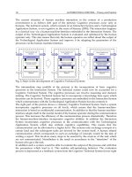
In the model proposed by Baum-Beneking [97]
the
discontinuity in the
field at
y
=
L
-
1,
(or
y'
=
0)
was removed by assuming that at
V
=
vd,,,,
the field
€
=
gP.
Therefore, the boundary conditions given by
Eq.
(6.187)
are now modified as follows
vdsat
at
y=
L-
/d
(y'=O)
vds
at
y=L
(y'
=
Id)
(6.189)
where the lateral field at the transition point. Assuming
€p
at
V,,
=
V,,,,,
the field becomes continuous from the linear to saturation region (see
Figure 6.29). Again solving the Poisson
Eq.
(6.186), under the above
boundary conditions, results in the following expression for
I,
(6.190)
This
is
the equation for
1,
used in the SPICE Level
3
model. In a more
elaborate formulation [98]-[
1001
mobile charges are included
in
Eq.
(6.185),
L-
1,-
LY
I
Fig. 6.29 Electric field along the channel
of
a
MOSFET
assuming field at a point
P
is
(a)
infinite (very large) (dotted line) and
(b)
finite value
gP
(continuous line)
298
6
MOSFET
DC
Model
that is,
(6.191)
where
X,
is the mean depth of current spreading near the drain end. This
equation when solved under the boundary condition (6.189) yields
where
b
=
l/qNb
WvsatXo.
Again when
b
=
0
(i.e., no mobile carriers in the
depletion region),
Eq.
(6.192) reduces
to
Eq.
(6.190). Note that using either
Eq. (6.190) or (6.192), the slope at the transition point will
be
discontinuous.
The
CLM
models described above, though different in their exact formula-
tions, all predict a constant field gradient in the
CLM
region due to the
constant term in the right hand side of
Eq.
(6.185). However, using a
2-D
device simulator it has been found that the channel field rises exponentially
towards the drain. Thus, due to the incorrect channel field calculations,
these models do not predict device output conductance accurately. This
inaccuracy in the device output conductance is of more concern for analog
circuit design than for digital design. For analog design,
a
more accurate
expression for the channel field is thus desirable. An accurate knowledge
of the field, particularly the maximum field, is also important for modeling
substrate current, as we will see later in Chapter 8.
The inaccurate field calculation in tbe above models stems from the fact
that we have ignored the oxide field in the analysis.
To
take the oxide
field
into account both empirical and pseudo-two dimensional analysis has been
used.
Empirical Model. An empirical model that has been widely quoted
to
account for the
CLM
effect is the model proposed by Frohman-
Bentchkowsky and Grove
[95],
according to which
'ds
-
vdsat
1,
=
Qi
(6.193)
where
bi
is the average transverse electric field near the drain depletion
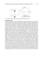
region at the Si-SiO, interface and is the result of the following three fields
(see Figure 6.30):
The field
6,
in the depletion region due to the
pn
junction comprised
of
the
n+
drain region and the p-substrate. Thus,
6.7
Short-Geometry Models
299
Fig.
6.30
Electric field distribution
for
a MOSFET operating in saturation showing
components
&,,g2
and
g3
of
the transverse field
&,
The fringing field
b,
due to the potential difference
V,,
-
Vi,,
between
the drain and the gate, where
V$,
=
V,,
-
Vfb.
Thus,
where
A,
is
the empirical fringing field factor associated with the field
6,.
The fringing field
€,
due to the potential difference
V$,
-
V,,,,
between
the gate and the end of the inversion layer. Thus,
where
A,
is the empirical fringing field factor associated with the field
G,.
The total field
Q,
=
Q,
+
&2
+
6,.
Typical values for
A,
and
A,
are
0.2
and 0.6, respectively. This model incorporates a rather complete theory
on
the
CLM
supported by experimental data. Equation (6.193) for
1,
has been
used by many others [18],
[loll.
Pseudo-2D
Model.
The approach used by Frohman-Bentchkowsky and
Grove is purely empirical.
A
more physical approach to calculate
CLM
factor
1,
was proposed by El-Mansy and Boothroyd
[
1021 and subsequently
modified by others who also took into account the shape of the source/drain
structures 1621,
[
1041.
A
simplified form, that retains the essential features
of
these models, is summarized here.
The cross-section of the drain region, where the
CLM
effect is taking place,
is
shown schematically in Figure
6.31.
To simplify the mathematics it is
assumed that
(1)
the drain and source junctions are square in shape, (2)
the drain current
is confined to flow within the depth
of
the junction
,
and
(3) the velocities
of
all carriers in the drain region are saturated. Assumption
(2)
limits the validity of the present analysis to conventional source/drain
junctions, but the analysis can easily be extended to
LDD
junctions
As
shown in Figure 6.31, the drain region is bounded on one side by the
line
AB,
which marks the beginning of the velocity saturation region, and
[
1031-[109].
300
6
MOSFET
DC
Model
GATE
SAT
U
R
AT
10
N
4
DRAIN
1
L
-
- -
-
- -
-
-
-
-
-
D
C
0
WY'
L
4J-4
Fig. 6.3
1
Schematic diagram illustrating analysis
of
the velocity saturation region
on the other side at the drain junction edge by CD. Since there are no
field lines crossing the line CD, the space charge is controlled only by the
electric fields crossing the other 3 sides of the rectangle. Applying
Gauss'
law to the volume with sidewall
ABCD
and unit width
W
we get
(6.194)
where
Q,
is the mobile charge density in the drain region and
box
is the
gate oxide field given by
4
Qm
=-NbXjy
+
-y
EOEsi
EOEsi
(6.195)
Lox
Differentiating Eq. (6.194) with respect to
y
we get
(6.196)
Since the velocity of the mobile carriers is assumed to be saturated in the
drain region, the mobile charge density
Qm
equals that at the point of
saturation where
V(y)
=
V,,,,.
Therefore, from simple charge control
analysis we get [cf. Eq. (6.43)]
(6.197)
d€,(Y)
€0,
4
Qm
Xj
7
+
-
&ox(O,
y)
=
__
NbX
j
+
Esi
E&si
E&si
Qm
=
CoxCVgs
-
Vfb
-
20f
-
Vdsatl
-
qNbXj.
Combining
Eqs.
(6.195)-(6.197) we get
(6.198)
6.7
Short-Geometry
Models
301
where
(6.199)
The right hand side of Eq. (6.198) is the amount of charge released by the
oxide field as a results of a rise in the channel voltage equal to
(V(y)
-
Vd,,,),
while the left hand side is the corresponding increase
of
the channel field gradient in order to support these charges. Redefining the
coordinate system
as
y’
=
0
at point
D
and
y’
=
1,
at point C, and solving
Eq.
(6.198) under the boundary condition
we get
&,(y’)
=
8,
cosh
(;)
(6.200a)
V(y’)
=
+
/bc
sinh . (6.200b)
Equation (6.200) shows that the channel field increases exponentially
towards the drain. Extensive 2-D numerical analysis confirms the basic
form of Eq.(6.200). At the drain end
of
the channel where the field is
maximum, denoted by
b,,
we have
(5)
(3
6,
=
&,(y’
=
1,)
=
6,
cash
-
(6.201a)
Vds
=
Vd,,,
+
18,
sinh
-
(6.20 1
b)
Using the identity sinh2
A
+
1
=
cosh2
A,
Eqs. (6.200) and (6.201) can be
combined to give the following expression for
1,
and
6,
in the channel
(9
(6.202a)
(6.202b)
Further simplification for
1,
can be obtained if we approximate
8,
as
(6.203)
302
6
MOSFET
DC
Model
where
6‘
allows
6,
to fit more
closely
with
Eq.
(6.202b). With this approxi-
mation,
Eq.
(6.202) for
1,
simplifies to
(6.204)
where
V,
=
l&J(l
+
S’C?~) and can be treated as a fitting parameter. This
equation has been shown to fit the conductance very well [116].
Remarks on the Continuity
of
the Current and Conductance at the Transition
Between the Linear and Saturation Regions.
Any
of
the
1,
expressions
discussed here, when used in Eq. (6.182) or (6.183) result in a discontinuity
of
the slope at the transition point from linear to saturation region. This
obviously is not desirable for circuit models. This discontinuity of the slope
at the transition point can easily be removed by introducing an additional
condition to be satisfied, that is
(linear region)
$1
Vas=
Vasat
- -
(saturation region). (6.205)
With condition (6.205) satisfied, the parameter
&,
or
&,
(one
of
them if
both are used) in
1,
expressions can no longer be a fitting parameter, since
its value will be dictated by the condition (6.205). Though this condition
ensures that the first derivative will be continuous, it does not guarantee
that the conductance
gds
will be smooth.
For
gd,
to be smooth, the second
derivative
of
I,,
must be continuous at
Vd,
=
Vd,,,. Although a drain current
model having a continuous conductance is not necessary for simulation of
digital circuits, it is important for analog circuit simulation.
Another approach that ensures continuity
of
the drain current derivatives
at the transition point from linear to saturation region is to introduce the
following empirical function
$1
ydS
=
Vdsat
(6.206)
where
B
=
ln(1
+
e”).
Figure 6.32 shows
a
plot of the function
F(Vds,
V,,,,)
versus
(Vds/Vdsat)
for
3
different values of the parameter
A.
Large values of
A
yields steep transitions
between the linear and saturation regions while small values result in
smooth transitions. The value of
A
=
10 has been found to be a good choice
[118]. The effective drain-source voltage
V,,,,
which results in a smooth
6.7
Short-Geometry
Models
303
1.21
1
I,
I,
I
,
T
,I
Fig.
6.32
Variation
of
the function
F(Vds,
V,,,,)
[Eq.
(6.206)]
as a function of
Vds/Vdsa,
for
different
values
of
A
transition from linear to saturation region, becomes
(6.207)
By replacing
V,,
with
V,,,
in the current Eqs. (6.169) and (6.182), a smooth
transition is observed. This also ensures a smooth
gds.
The use of
V,,,
for
V,,
not only insures smooth current and conductances, but it also reduces
two drain current equations in the linear and saturation regions of device
operation to
a
single current equation as follows
1).
1
V,,,
=
V,,,,
{
1
-
In
1
+
eA(1
-~ds/~dsat)
Note that in this approach
1,
is used for both the linear and saturation
regions and
V,,
is replaced by
V,,,
everywhere including
1,.
Equation
(6.208)
predicts that output resistance
R,(=
l/gds) of
a
short
channel
MOSFET
in saturation increases with increasing
V,,
due to
increasing
1,.
However, in real devices, particularly nMOST,
R,
increases
only up to moderate
V,,
(beyond
V,,,,),
and at higher
V,,
it starts
to
decrease
(see Figure 7.21, which is a plot of
gds
vs.
V,,).
This decrease in
R,
is induced
by
the hot-carrier substrate current
I,
(cf. section 3.4; also see chapter
8).
The substrate current created near the drain flows towards the substrate
contact and produces a voltage drop across the substrate resistance along
its path
as
shown
in
Figure 6.33a. This voltage drop forward biases the
304
6
MOSFET
DC
Model
channel causing a reverse body-bias effect, which lowers the device threshold
voltage
V,h
and thereby increases the drain current. DIBL also causes
Kh
to decrease, but the effect is much smaller and in general affects the drain
current only near
V,h
(cf. section
5.3).
In general, all three mechanisms
-
CLM, DIBL, and hot-carrier effect
-
affect the
MOSFET
output resistance,
but their relative contributions strongly depend on the bias condition as
shown in Figure 6.33b.
To
a first order the increase in the drain current,
or decrease in the output resistance, can be modeled by including hot-
electron induced substrate current
I,
as
[62]
=
Ids
+
(for
Ids
'
Idsat)
(6.209)
where
A
is a fitting parameter. The expressions
for
I,
are discussed in
Chapter
8.
",
P
'd
r
5
.o
10.0
DIBL
(b)
Vk
(VOLTS)
Fig.
6.33
(a) Schematic diagram to illustrate the effect
of
substrate current
to
MOSFET
output resistance.
(b)
Drain current
I,,
vs.
drain voltage
Vds
of
a nMOST showing the
dominant mechanisms affecting the current in different bias regions. (After
KO
[62])
6.7
Short-Geometry
Models
305
6.7.4
Subthreshold Model
For short channel devices, the surface potential
4,
is not constant along
the length
of
the channel (see Fig.
5.25).
Although the drain current remains
exponentially dependent on the gate voltage, various physical arguments
used in the derivation of
(6.104)
no
longer apply (cf. section
5.3.3).
Never-
theless, for short-channel subthreshold current calculations most of the
CAD models use slightly modified form of Eq. (6.104) or
(6.105).
Since short-
channel subthreshold currents show strong dependence on
V,,,
it is normally
included
in
the effective gate drive through the
DIBL
effect. Thus,
v,,,
in
Eq. (6.104)
is
replaced by
V,,,
[cf. Eq. (6.168a)l. Once
V,,
is replaced by
V,,,,
the different short-channel subthreshold current models differ only in the
prefactor term
I,,
[84], [1lO]-[115]. Starting from the diffusion current
expression for n-channel [cf. Eq. (6.91)], it has been shown that
I,,
for short
channel devices can be approximated as [cf. Eq. (6.97)] [llO]-[115].
I
ds
- -
qWDnT;hnse(", ",,,)/i,",(l
-
ep"ds/vt)
(6.2 10)
where
D,
is the electron diffusion constant,
n,
is the electron concentration
in the channel at the source, and
fch
is the average channel thickness given by
Leff
where
['
is a fitting parameter which accounts for the fact that the real
channel thickness is somewhat bigger than that derived from the square
root term in the above equation. In the above equation
6,
is the average
surface potential and can be replaced by an average value of
0.5
[llo],
is given by
70
i-
'-1+ioJm
where
i0
and
q0
are some fitting parameters. Finally,
Leff
in Eq. (6.210) is
given by
(6.211~1)
where
X,,
and
X,,
are the source and drain depletion widths, respectively,
at the surface, given by
Leff
=
L
-
Xs,
-
X,,
(6.211b)
and
(6.211~)
306
6
MOSFET
DC
Model
where is the sourceldrain to bulk built-in potential, given by Eq.
(3.3).
Compare Eqs. (6.211a) and (6.21 lb) with Eq. (5.95), the depletion region
expressions between the sourceldrain to substrate pn junctions.
In the BSIM model the prefactor term,
I,,
=
bV:exp(1.8), is an empirical
factor that is based on matching the experimental data with the model
[25]. Often in CAD models, Eq. (6.105) is also used for short-channel
I,,
with
m
and
r]
regarded as fitting parameters.
Transition from the Weak
to
Strong Inversion Region. Accurate modeling
of
the transition region can be achieved by including both drift and diffusion
currents simultaneously without distinguishing between
the
weak and strong
inversion regions. However, this leads to a more complicated equation for
the current. Therefore, for circuit models, various simplified approaches
have been suggested. In one approach, the following approximate formula
is used to ensure continuity
of
the current from weak to strong inversion
(6.2 12)
where
Id,,, is the strong inversion current due to the drift only such as
given by Eq. (6.84) or (6.208). Equation (6.212) matches the following two
extreme cases:
0
When
V,,
<<
VIh,
Id,,,
is zero
so
that Eq. (6.212) reduces to
or
=I
e(vgs-Vth)/tlVt(l
-
,-Vds/Vt)
PS
which
is
the same as Eq. (6.104).
When
V,,
>>
Vth,
the drift current
Id,,,
is
much larger than the diffusion
current
I,,
and therefore, Eq. (6.212) reduces to
Ids,t
=
Id,,,.
Equation (6.212) models the transition region fairly accurately:
In the approach used in the SPICE Level 4 model (BSIM), the transition
region is modeled based on the fact that when
V,,
is increased above
VIA,
the subthreshold current approaches a constant value. This imposes an
upper limit on the subthreshold current. This limiting current applies when
V,,
>
3Vt above
V,,
and is obtained from the current in the saturation
region with
Vqs
=
V,h
+
3Vt,
so
that
(6.213)
and the weak inversion, or subthreshold current,
is
modeled
as
(6.214)
Isub'subO
Ids,w
=
Isub
+
IsubO
6.7
Short-Geometry Models
307
where
lsub
is given by
Eq.
(6.104). The total drain current from weak
to strong inversion now becomes [25]
(6.215)
where
In still another approach the transition region, bounded by gate voltages
Vgxl
and
VgX2
between weak and strong inversion, is modeled by a third
order polynomial of the following form [112]
IdsJ
=
Ids,w
+
Ids,s
and
Ids,,
are given by
Eqs.
(6.214) and (6.84), respectively.
(6.2
1
6)
where the coefficients
a,
b,
c
and
d
are calculated from log(lds) and its
derivative with respect to
Vgs
at two end points
(V,,,
and
V,,,)
of the
transition region. Although this approach results in a continuous and
smooth transition, the accuracy of the simulation in the transition region
is totally dependent on the accuracy
of
the function values and their slopes
at the two end points.
Of
the three approaches used to model the transition
region, the one given by Eq. (6.212) is used by many others and seems to
work well.
6.7.5
Continuous
Model
The short channel models discussed
so
far are piece-wise model where
different equations are used for different regions of device operation. In
order to ensure that the current and its (at least) first derivatives are
continuous at the transition points smoothing functions are often used.
Thus, by using smoothing functions (6.122) and (6.207), one arrives at the
following equation
and is obtained by replacing
V,,
in
Eq.
(6.208) with
V,,,
given by Eq. (6.122).
This is single equation which
is
valid in all region of device operation.
Figure 6.34a shows measured and simulated
Id,
-
Vds
characteristics for a
p-channel device fabricated using submicron CMO? process with
Wm/Lm
(drawn dimensions in pm)
=
10/0.5 and
to,
=
105 A. Circles are experi-
mental data points while continuous lines are based on Eqs. (6.142), (6.174)
and (6.204) for
p,,
Vds,,
and ld, respectively. The corresponding
Id,
-
Vd,
and
I,,
-
Vgs
characteristics for n-channel device are shown in Figures 6.34b
and 6.34c, respectively. In this case
Eq.
(176) was used for Vd,,,. Best fit to
the data was obtained using nonlinear optimization method as discussed
later in section 10.6. The extracted value of
usat
is 8
x
lo6
cmjs for nMOST
while the corresponding value for pMOST is 6
x
106cm/s. These values
are consistent with those measured experimentally as discussed in section
6.6.2. Note from Figures 6.34, while n-channel devices get velocity saturated
308
3
.O
6 MOSFET
DC
Model
I I
1
I
I I
pMOST
toX
=
105
A
W,/L,
=
10l0.5
v,,
=
-4
v
h
c
E
4
v
U
I
1
.o
I
-
-2
v
0.01
-1-
-
7-
-1-
-
i
-
I
*
"
0.0
0.5
1.0
1.5
2.0 2.5
3.0 3.5
-Vh
(VOLTS)
(a)
1,
=
105
A
w,,,/L,
=
10D.25
1.0
-
0.0
0.5
1.0 1.5
2.0 2.5
3.0
3.5
0.0
r
-1"
-
1
.
I_
,
.
,-
.
,
Vb
(VOLTS)
(b)
Fig. 6.34 Measured and calculated
I
-
V characteristics
of
a MOSFET fabricated using
submicron CMOS n-well process
(tax
=
150
A).
(a) p-channel output characteristics at
vb,
=
ov,
(b) n-channel output characteristics at two
vb,,
and (c) n-channel transfer charac-
teristics for different channel lengths.
All
dimensions are drawn. Symbols are measured
data, while lines are those calculated using
Eq.
(6.217)
6.7 Short-Geometry Models
309
I
I
jU)I
nMOST
'
I
(c)
Fig. 6.34 (continued)
and have very little
CLM
effect, the corresponding p-channel devices have
more
CLM
effect and less velocity saturation effect for the same applied
field. The model fits the data fairly well with an average error of less than
3.0%
for
VqS
>
V,,
over series
of
different length and width devices and back
biases. However, for
V,,
<
V,,
the average error is over
15%
due to large
errors in the moderate inversion region14 (near
V,,,).
In fact all piece-wise
models have generally high errors in this region.
The long channel charge-sheet model (cf. section
6.3),
which is inherently
continuous in all regions of device operation and is also accurate in the
moderate inversion region, has been extended for short channel devices
[17]-[19].
However, they are not generally used for
VLSI
simulations for
reasons discussed in section
6.3,
though they are being used for circuit
simulations, particularly analog applications, when computation time is not
of prime concern. The drain current models for narrow width devices are
the same as for short channel devices, provided proper threshold voltage
model for narrow widths (cf. section
5.3.2)
is
taken into account
[llS].
If the model is physically based, then a single set of model parameters
should fit different geometry devices. However, often we introduce empirical
l4
It
should be pointed
out
that the calculated current (continuous lines) shown in
Figure 6.34b also takes
into
account the source/drain resistance,
as
discussed in
section 6.8.
310
6
MOSFET
DC
Model
parameters in the circuit models in order to acheive good computation
efficiency as well as accuracy. For this reason, many electrical parameters
become geometry dependent. The most commonly used formulation for
the geometry dependence of an electrical parameter
P
is [120]
p,
p,
P
=
Po
+-+
-
LW
where
Po,
PI
and P, are fitting parameters. The
BSIM
model has
9
of
its
parameters given by the above equation (see section 11.5)
.
While using such
equations one must be careful in extracting the length and width dependent
parameter values.
6.8
Impact
of
Source-Drain Resistance
on
Drain Current
In
the discussion
so
far we had implicitly assumed that the voltage applied
at the terminals
of
the device are the same as that across the channel region.
In
other words, the voltage drop across the source/drain region is negligible
compared to the voltage applied at the terminals.
As
was discussed in
section 3.6.1, this indeed is true only for long-channel devices. For
short-channel devices, the impact
of
source/drain resistance is a reduction
of
the transconductance
gm
and device current driving capability.
The effect of the source and drain resistance
R,
and
Rd,
respectively, in
calculating
Id,
can be understood from the equivalent circuit shown in
Figure 6.35. Clearly the effective drain and gate voltages
V&,
and
V$,,
respectively, are reduced below the voltages
Vd,
and
V,,
applied at the
external terminal
of
the device by the voltage drop across these resistors;
that
is,
(6.218a)
(6.218b)
5,
=
Vgs
-
IdsR,
vds
=
‘ds
-
IdsR,
Fig.
6.35
MOSFET
showing internal and external terminal
resistance is taken into account
voltages when sourceidrain
6.8
Impact
of
Source-Drain Resistance on Drain Current
31
1
where
Ri
=
R,
+
Rd.
It is generally assumed that
R,
=
Rd
=
Ri/2.
Often
circuit models
(SPICE
Levels
1-3)
treat this effect
of
Rs
and
Rd
as
an
external component of the device by including two additional nodes per
transistor. However, this results in extra computational time. Rather than
considering these resistors
as
external simulation elements, one can incor-
porate them into the device model explicitly, thereby reducing the computa-
tional time. This is the approach normally used in most
of
the recently
developed device models, including SPICE Level
4
model. Although
Rs
and
Rd
are gate bias dependent, particularly for
LDD
devices (cf. sections
3.6.11,
in
what follows we will assume them to be bias independent. In spite
of
this assumption, the explicit inclusion of
R,
and
Rd
in an analytical drain
current model results in a complex equation for
Id,
as seen below.
In terms of the intrinsic voltages, the linear region drain current model for
short-channel devices is given by
(6.2 19)
where we have replaced
Vg,
and
Vd,
of
Eq. (6.169) by the intrinsic voltages
Vgs
and
V&,,
respectively, and
0,
=
(L&J1.
Using
Eq.
(6.218) in (6.219), it is
easy
to see that resulting equation in
Id,
with explicit
R,
and
Rd
will be
difficult to solve. However, remembering that
0,
8b,
and
0,
are small
so
that
the terms involving their products can be neglected, one can write the
above equation
as
Equation (6.220) is quadratic in
Ids
and can now be solved for
Id,
giving
(6.221)
where
a,
=
0.5PO(1
-
a)R:
+
0.58Rt
+
OcRt
a3=
fl
0
(V
g
-
0.5ctViJ
vgi
=
Vgs
-
Vih.
(6.222a)
a2
=
1
+
(6
+
PoRt)T/St
+
ebvsb
(0,
+
0.5RJo
-
afloRi)vds
(6.222b)
(6.222~)
(6.223)
In general, the term
a,
is
much smaller than the other terms and in
practice one often meets the condition [121]
-
<
0.1.
a1a3
312
6
MOSFET
DC
Model
Using typical values for the parameters
8,
Ob
and
Q,,
the above condition,
in a more practical form, becomes
Id,R,
<
0.5V.
If
the above condition is satisfied than the square root term in
Eq.
(6.221)
can be expanded. Retaining the first two terms in the Binomial expansion
of the expression under the square root, we get
(6.224)
where
e:
=
O,
-
p,~,
(a
-
0.5).
The expression for
Id,
in saturation is even more cumbersome. Since R,
degrades
gm
in the linear region more severely than in the saturation
region (cf. section 3.6.1), circuit models usually include
R,
only in hear
region current models.
When the effect of carrier velocity saturation is not important
so
that
0:
can be ignored, then Eq. (6.224) can be approximated
as
(6.225)
The first order equations (6.224) and (6.225) clearly show that the effect of
R,
is to reduce the drain current and hence the transconductance
9,.
For
long channel devices PoR,
=
0,
which implies that the current is almost the
same as if series resistance
R,
is zero. However, for short-channel devices
the
P,R,
term is not negligible, and therefore the effect of series resistance
must be taken into account. From Eq. (6.225) we see that mathematically
the effect of
R, is the same as
of
reducing the effective mobility
,us
due to
the vertical field. Therefore,
in circuit models the eflect
of
R,
is simply modeled
by replacing mobility degradation factor
6
with
(6
+
B,R,)
in the drain current
equations.
Note that replacing
6
with
O+&,R,
not only affects the linear region
current, but also reduces short channel current in the saturation region.
This is because for short channel devices,
V,,,,
depends upon
ps
through
6,
=
uSat/ps.
Since
R,
reduces
,us
which in turn increases
&,,
it results in an
increase in the
V,,,,
[cf. Eq. (6.174)]. The modeled
Id,
-
Vds
characteristics
(continuous lines) shown in Figures 6.33 and 6.34 were based on inclusion
of
R,
through
ps.
6.9
Temperature Dependence
of
the Drain Current
313
6.9
Temperature Dependence
of
the Drain Current
MOS
transistor characteristics are strongly temperature dependent.
Modeling the temperature dependence of the MOSFET characteristics is
important in designing VLSI circuits since, in general, an IC is specified
to be functional in a certain temperature range, for example
-
55
"C
to
125
"C. In addition, operating the
MOSFET
below room temperature (low-
temperature operation) results in improved device performance; a factor
of two improvement in switching speed can be achieved by operating a
1
pm
device at
77
K
(-
196
"C)
[122]-[124]. However, device degradation due to
hot-carrier effects also increases with decreasing temperature (see section
8.6) [124].
The
MOSFET
drain current varies considerably with temperature. The
change in drain current in the temperature range 0-100
"C
for a typical
n-channel device is over
20%,
being slightly lower for the corresponding
p-channel device. The temperature coeficient
of
the drain current can be
positive, negative,
or
zero depending upon the operating voltages. This is
shown in Figure 6.36 where measured
JIds
in saturation is plotted against
gate voltage
for-different
temperatures for a nMOST with
WJL,
=
9.4/9.4
(pm),
to,
=
105
A,
and
V,,
=
0.56
V.
The Zero Temperature Coefficient (ZTC)
0.76
-
-
GATE AND DRAIN SHORTED
l11'l~1'1'l~I
GATE
VOLTAGE,
Vq5
(V)
Fig.
6.36
Variation
of
Ids
versus V, in saturation region
of
device operation with temperature
as a parameter. It
shows
temperature coefficient
of
I,,
is either positive, negative, or zero
depending upon the operating bias
314
6
MOSFET
DC
Model
of
the drain current could be either in the linear
or
saturation region
of
device operation. The gate voltage, which leads to
ZTC
is very close to the
device threshold voltage, as we shall see shortly.
The negative temperature coefficient of
I,,
(at higher temperatures) is
primarily due to (1) decrease in the carrier mobility, (2) increase in the
threshold voltage (cf. section 5.4), and
(3)
decrease in the carrier saturation
velocity. There are many other parameters which are temperature
dependent [126], but if the drain current model is physically based one
can easily explain the temperature dependence of the current using the
above three parameters. The positive temperature coefficient of
I,,
occurs
when the device is operating in the weak and moderate inversion region
and is primarily due to an increase in the intrinsic carrier concentration
ni, in accordance with Eq. (6.96b) [127], [l28].
6.9.1
Temperature Dependence
of
Mobility
Carrier mobility in the inversion layer is strongly temperature dependent.
The temperature dependence of the mobility has been traditionally used
to extract contributions from different scattering mechanisms. For high
quality devices, electron surface mobility
p,
may range from 600 cm2/V.s at
room temperature to 20,000 cm2/V.s at 4.2
K.
Since different scattering
mechanisms are effective in different ranges of temperature, circuit
simulators normally use different mobility models for different temperature
ranges. For
T
>
200 K, the most commonly used temperature dependent
mobility model is [59], [124]
(6.226)
which is valid for both p- and n-channel devices, provided the field is not
very high
(<
8
x
lo4
V/cm).
In
general
8
is
a
weak function
of
temperature;
therefore, its temperature dependence
is
generally ignored.
A
comparison
of Eq. (6.226) with experimental data is shown in Figure 6.37. Note that
for p-channel devices the linear relationship between
l/ps
and
&eff
remains
valid even at low temperatures, which indeed
is not the case for n-channel
devices. However, for thin gate oxides and higher gate voltages (high fields),
it is more appropriate to use the following equation for mobility [28], [64]
(6.227)
where
8,
and
6,
are functions
of
temperature and have been obtained by
fitting the data to the model over a wide temperature range
[28].
It has been observed that the functional form of the temperature dependence
of low field mobility
po
is
T-";
that is,
po
at any temperature T, in the
6.9
Temperature Dependence
of
the Drain Current
-
3.00-
E
<
'?
-
>
t
2.00-
z
N
m
315
I
<=400K
nMOST
300
K
~
0
one
273
K
85.00
-
pMOST
T
=
300K
-
-
N
E
Y
t
'?
Do o
d.
0
c
45.00!
-
77K
5.00
I
1.001
I
0.05
0.20
0.:
5
Fig.
6.37
Inversion layer mobility versus normal effective field at different temperatures
(a)
n-channel
MOSFET
to,
=
310A
and
(b)
(b)
p-channel
MOSFET
to,
=
250k
Solid lines
represent
Eq.
(6.226)
while symbols corresponds to experimental data. (After Arora and
Gildenblat
[59])
temperature range
200-400
K can be expressed as
I
I
(6.228)
where
m
is
the slope of the line fitted to the low field mobility
po
versus
temperature Tcurve plotted
on
log-log scale, and
To
is
the nominal or
reference temperature. For p-channel devices, the value of
m
lies in the
range
1.2-1.4
while
for
n-channel devices it ranges between
1.4
to
1.6
for
the temperature range between
200 K-450 K.
The value of
m
is
a function
316
6
MOSFET
DC
Model
of
the gate field at which the mobility is measured and it tends to be
higher at lower fields. The observed difference between the temperature
dependence of the
n-
and p-channel mobilities is because electron and hole
scattering processes are different. SPICE uses Eq. (6.228) with
m
=
1.5 for
both
p-
and n-channel devices. Assuming
m
=
1.5, Eq. (6.228) yields the
following expression for the temperature coefficient of mobility
1
dp
1.5
pdT-
T'
-~
(6.229)
Temperature Dependence
of
Threshold Voltage.
The temperature coefficient
of
V,h
is approximately 1 mV/"C for modern CMOS devices as was discussed
in section
5.4.
Recall that the threshold voltage exhibits a linear depen-
dence on temperature over a wide temperature range. Threshold voltage
Vth
increases with increasing temperature, and therefore, drain current
decreases.
Zero Temperature Coeficient
of
Drain Current.
Differentiating the classical
saturation drain current equation (6.57) with respect to the temperature
T,
yields the following equation
(6.230)
The gate voltage which corresponds to zero temperature coefficient (ZTC)
of
Ids
is simply obtained by equating above equation to zero. Combining
the resulting equation with (6.229) yields
dVth
V
=I/
-__~
dT
0.75'
gs
th
(6.231)
Assuming
dV,,/dT
=
1
mV/"C, it is easy to see that the gate voltage corre-
sponding to ZTC of
Id,
is very close to
Kh.
Similar results are obtained
if we use the linear region current equation.
Negative Temperature CoefJicient
of
Drain Current.
For long channel devices,
temperature dependence of
Id,
is accurately modeled using only the tem-
perature dependence of
po
and
Vth.
However, for short channel devices one
needs to take into account the temperature dependence
of carrier saturation
velocity
usat
or
saturation field
6,.
The following linear relation for
usat
fits
the data well [119]
(6.232)
where
usat(To) is the value of
usat
at
T
=
To and
P,
is a fitting constant.
Figure 6.38 shows temperature dependence of
Id,
for a p-channel device
usat(T)
=
usat('o)
-
PAT
-
To)
6.9 Temperature Dependence of the Drain Current
317
0.0
1
.O
2.0
3.0
4
Drain
Voltage
-
V,
(V)
Fig.
6.38
Measured
and calculated output characteristics at two temperatures
(W,/L,
=
10/0.75,
to,
=
105
A)
at
25
"C and
100°C.
Circles are experimental
data
while
continuous lines are calculated current based on
E,q.
(6.208).
The only parameters that have been
changed
from
25
to
100
"C
are
Vfh,
po
and
us,,.
It
should
be
pointed out that
if
the drain current model is not
physical,
but
more empirical in nature, then in order
to
fit
the data
well,
one probably requires more temperature dependent parameters than
discussed here.
GATE
VOLTAGE,
(V)
Fig.
6.39
Device
I,,
-
V,,
characteristics
in
the subthreshold
or
weak inversion region at
different temperatures. (After Gaensslen et al.
[
1221)
318 6 MOSFET DC Model
Positive Temperature Coefficient
of
Drain Currents.
As
temperature
increases, the subthreshold current increases [cf.
Eq.
(6.96b)I resulting in
a decrease in the subthreshold slope. Figure 6.39 shows drain current as
a function of gate voltage showing subthreshold behavior as a function
of
temperature
[122].
Note that the subthreshold slope
S
has decreased from
86 mVJdecade at 296
K to
22
mVJdecade at
77
K. This shows that the device
can be turned-off much more easily at
low
temperatures than at high
temperatures. This is the
so
called positive temperature coefficient
of
I,,
and can be modeled fairly accurately using
Eq.
(6.104).
References
[l]
S.
Selberherr, A. Schutz, and
H.
W. Potzl, ‘MINIMOS-A two-dimensional MOS
transistor analyzer’, IEEE Trans. Electron. Devices, ED-27, pp. 1540-1550 (1980).
[2] M. R. Pinto, C.
S.
Rafferty, and R. W. Dutton, ‘PISCES-11: Poisson and continuity
equation solver’, Stanford Electronic Lab. Tech. Rep., Sept. 1984.
[3] C.
L.
Wilson and
J.
L.
Blue, ‘Two-dimensional finite element charge-sheet model of
a short channel MOS transistor’, Solid-state Electron., 25, pp. 461-477 (1982).
[4]
H.
C. Pao and C. T. Sah, ‘Effects of diffusion current on characteristics
of
metal-oxide
(insulator)-semiconductor transistors’, Solid-state Electron., 9, pp. 927-937
(1
966).
[5] R. F. Pierret and
J.
A. Shields, ‘Simplified long-channel MOSFET theory’, Solid-state
Electron., 26, pp. 143-147 (1983).
[6] A. Nussbaum,
R.
Sinha, and D. Dokos, ‘The theory
of
the long-channel MOSFET’,
Solid-state Electron., 27, pp. 97-107 (1984).
[7]
J.
R. Brews,
‘A
charge sheet model
of
the MOSFET’, Solid-state Electron., 21, pp.
[S]
J.
R. Brews, ‘Physics
of
MOS transistor’, in
Silicon Integrated Circuits,
Part A, Ed.
D. Kahng, Applied Solid-state Science Series, Academic Press, New York, 1981.
[9] P.
P.
Guebels and F. Van de Wiele,
‘A
small geometry MOSFET models for CAD
applications’, Solid-state Electron., 26, pp. 267-263 (1983).
[lo]
G.
Baccarani, M. Rudan, and G. Spadini, ‘Analytical i.g.f.e.t model including drift
and diffusion’, IEE
J.
Solid-state and Electron Devices, 2, pp. 62-68 (1978).
[11] F. Van de Wiele, ‘A long channel MOSFET model’, Solid-state Electron., 22, pp.
r121 C. Turchetti and
G.
Masetti. ‘A .CAD-oriented analytical MOSFET model for
345-355 (1978).
991-997 (1979).
L_.
high-accuracy applications’, IEEE Trans. Computer-Aided Design, CAD-3, pp. 117-
122 (1984).
[13] A. M. Ostrowsky,
Solutions
of
Equations and Systems
of
Equations,
Academic Press,
New York, 1973.
[14] Y. Tsividis, ‘Moderate inversion in MOS devices’, Solid-state Electron., 25, pp.
1099-1104 (1982), also see “Erratum”, Solid-state Electron., 26, p. 823 (1983).
[l5] Y. P. Tsividis,
Operation and Modeling
of
the
MOS Transistor,
McGraw-Hill Book
Company, New York, 1987.
[16]
P.
P. Guebels and F. Van de Wiele, ‘A small geometry MOSFET models for CAD
applications’, Solid-state Electron., 26, pp. 263-267 (1983).
[17]
S.
Yu,
A.
F.
Franz, and T. G. Mihran,
‘A
physical parametric transistor model for
CMOS circuit simulation’, IEEE Trans. Computer-Aided Design, CAD-7, pp.
[18] H.
J.
Park,
P.
K.
KO,
and C. Hu, ‘A charge sheet capacitance model of short channel
1038-1052 (1988).
References 319
MOSFET’s
for
SPICE, IEEE Trans. Computer-Aided Design, CAD-10,
pp.
376-389
(1991).
[19]
A.
R. Boothryod,
S.
W. Tarasewicz, and C. Slaby, ‘MISNAN-A physically based
continuous MOSFET model
for
CAD applications’, IEEE Trans. Computer-Aided
Design, CAD-10, pp. 1512-1529 (1991).
[20]
C.
T.
Sah, ‘Characteristics of the metal-oxide-semiconductor transistors’, IEEE
Trans. Electron. Devices, ED-11, pp. 324-345 (1964).
1211 H. Schichman and
D.
A. Hodges, ‘Modeling and simulation of insulated-gate field-
effect transistor switching circuits’, IEEE
J.
Solid-State Circuits,
SC-3,
pp. 285-289
(1968).
[22]
H.
K.
J.
Ihantola and
J.
L. Moll, ‘Design theory of a surface field-effect transistor’,
Solid-state Electron., 7, pp. 423-430 (1964).
[23] A. Vladimirescu and
S.
Liu, ‘The simulation of MOS integrated circuits using
SPICET, Memorandum
No.
UCB/ERL M80/7, Electronics Research Laboratory,
University
of
California, Berkeley, October 1980.
[24]
H.
I.
Hanafi, L.
H.
Camnitz, and A.
J.
Dally, ‘An accurate and simple MOSFET
model for computer-aided design’, IEEE
J.
Solid-state Circuits, SC-17, pp. 882-891
(1 982).
1251
B.
J.
Sheu,
D.
L.
Scharfetter,
P.
K.
KO,
and M. C. Jeng, ‘BSIM: Berkeley short-channel
IGFET model for MOS transistors’, IEEE
J.
Solid-state Circuits, SC-22, pp. 558-565
(1987).
[26]
N.
D. Arora and L. M. Richardson, ‘MOSFET modeling for circuit simulation, in
Advanced
MOS
Device Physics
(N.
G. Einspruch and G. Gildenblat, Eds.), VLSI
Electronics: Microstructure Science, Vol. 18, pp. 236-276, Academic Press Inc.,
New York, 1989.
[27] H. C. de Graaff and
F.
M.
Klaassen,
Compact Transistor Modellingfor Circuit Design,
Springer-Verlag, Wien-New York, 1990.
[28] C L. Huang and
G.
Sh. Gildenblat, ‘Measurements and modeling of the n-channel
MOSFET inversion layer mobility and device characteristics in the temperature range
60-300K, IEEE Trans. Electron. Devices, ED-37, pp. 1289-1300 (1990).
[29]
M.
B. Barron, ‘Low level currents in insulated gate field effect transistors’, Solid-state
Electron., 21, pp. 293-309 (1972).
[30]
R.
M.
Swanson and
J.
D. Meindel, ‘Ion-implanted complementary MOS transistors
in low voltage circuits’, IEEE
J.
Solid-state Circuits, SC-7, pp. 146-153 (1972).
[31]
W.
Fichtner and
H.
W. Poetzl, ‘MOS modeling by analytical approximation. I.
Subthreshold current and threshold voltage’, Int.
J.
Electron., 46, pp. 33-55 (1979).
[32]
J.
B. Brews, ‘Subthreshold behavior
of
uniformly and nonuniformly doped
long-channel MOSFET’, IEEE Trans. Electron Devices, ED-26, pp. 1282-1291
(1979).
[33]
G.
T. Wright, ‘Simple and continuous MOSFET models
for
the computer-aided
design
of
VLSI’, IEE Proc.
I,
Solid-state and Electron Devices, 132, pp. 187-194
(1985).
[34] G.
T.
Wright, ‘Physical and CAD model for the implanted-channel VLSI MOSFET’,
IEEE Trans. Electron Devices, ED-34, pp. 823-833 (1987).
[35] C. Turchetti and G. Masetti, ‘Analysis of the depletion-mode MOSFET including
diffusion and drift currents’, IEEE Trans. Electron Devices, ED-32, pp. 773-782
(1985).
[36] G.
R.
Mohan Rao, ‘An accurate model
for
a depletion mode IGFET used as a load
device’, Solid-state Electron., 21, pp. 71 1-714 (1978).
[37] G. Baccarani, F. Landini, and B. Ricco, ‘Depletion-mode MOSFET model including
field dependent surface mobility’, Proc. IEE., 127, pt.
I,
pp. 230 (1980).
[38]
Y.
A.
El-Mansy, ‘Analysis and characterization
of
depletion mode MOSFET’, IEEE
J.
Solid-state Circuits, SC-15, pp. 331-340 (1980).
320 6 MOSFET DC Model
[39]
P.
Ratnam and A. B. Bhattacharyya, ‘Accumulation-punchthrough model
of
operation of buried-channel MOSFET’s’, IEEE Trans. Electron Device Lett., EDL-3,
[40] T. Yamaguchi and
S.
Morimoto, ‘Analytical model and characteristics
of
small
geometry buried-channel depletion MOSFETs’, IEEE
J.
Solid-state Circuits, SC-18,
[41]
S.
H.
Ahmed and C. A. T. Salama, ‘Depletion mode MOSFET modeling
for
CAD’,
IEE Proc. Part
I,
Solid-state
&
Electron Dev., 130, pp. 281-286 (1983).
[42] D. A. Divekar and
R.
I.
Dowell, ‘A depletion-mode MOSFET model for circuit
simulation’, IEEE Trans. Computer-Aided Design, CAD-3, pp. 80-87 (1984).
[43] D. Ma,
‘A
physical and SPICE-compatible models for the MOS depletion device’,
IEEE Trans. Computer-Aided Design, CAD-4, pp. 349-356 (1985).
[44] C.
Y.
Yu and
K.
C. Hsu, ‘Mobility models for the I-V characterstics
of
buried-channel
MOSFETs’, Solid-state Electron., 28, pp. 917-923 (1985).
[45] M.
J.
Van de To1 and
S.
G. Chamberlain, ‘Buried-channel MOSFET model for
SPICE‘, IEEE Trans. Computer-Aided Design, CAD-10, pp. 1015-1035 (1991).
[46] G. Merckel,
J.
Borel, and
N.
Z.
Cupcea, ‘An accurate large-signal MOS transistors
model
for
computer-aided-design’, IEEE Trans. Electron Devices, ED-19, pp. 68
1-
690 (1972).
[47] T. Ando, A. B. Fowler, and
F.
Stern, ‘Electronic properties
of
two-dimensional
systems’, Reviews
of
Modern Phys., 54, pp. 437-672, 1982.
[48]
D.
K.
Ferry,
K.
Hess, and P. Vogl, ‘VLSI Electronics: Microstructure Science,
Vol.
2
(N.
G. Einspruch, Ed.), p. 67. Academic Press, New York, 1981.
[49]
F.
N.
Trofimenkoff, ‘Field-dependent mobility analysis
of
the field effect transistor’,
Proc. IEEE, 53, pp. 1765-1766 (1965).
[SO] D. Frohman-Bentchkowsky, ‘On the effect
of
mobility variation on MOS device
characteristics’, IEEE Proc., 56, pp. 217-218 (1968).
[5l] A. G. Sabnis and
J.
T.
Clemens, ‘Characterization
of
the electron mobility in the
inverted (100) Si surface’, IEEE IEDM,
Tech.
Dig.,
pp.
18-21 (1979).
[52]
S.
C. Sun and
J.
D. Plummer, ‘Electron’ mobility in inversion and accumulation
layers on thermally oxidized silicon surface’, IEEE Trans. Electron Devices, ED-27,
[53] P. P. Wang, ‘Device characteristics
of
short-channel and narrow-width MOSFETs’,
IEEE Trans. Electron Devices, ED-25, pp. 779-786 (1978).
[54] M.
H.
White, F. van de Wiele, and
J.
P.
Lambot, ‘High-accuracy MOS models
for
computer aided design’, IEEE Trans. Electron Devices, ED-27, pp. 899-906 (1980).
[55]
K.
Y. Fu, ‘Mobility degradation due to the gate field in the inversion layer
of
MOSFETs’, IEEE Trans. Electron Device Lett., EDL-3, pp. 292-293 (1982).
[56] M.
S.
Lin, ‘The classical versus the quantum mechanical model
of
mobility
degradation due to the gate field in MOSFET inversion layers’, IEEE Trans. Electron
Devices, ED-32, pp. 700-710 (1985).
[57] M.
S.
Liang,
J.
Y. Choi, P.
K.
KO,
and C. M.
Hu,
‘Inversion-layer capacitance and
mobility of very thin gate-oxide MOSFETs’, IEEE Trans. Electron Devices, ED-33,
[58]
B.
Majkusiak and A. Jakubowski, ‘The dependence of MOSFET surface carrier
mobility on gate oxide thickness’, IEEE Trans. Electron Devices, ED-33, pp.
1717-1721 (1986).
[59]
N.
D. Arora and G. Sh. Gildenblat, ‘A semi-empirical model
of
the MOSFET
inversion layer mobility for low-temperature operation’, IEEE Trans. Electron
Devices, ED-34, pp. 89-93 (1987).
[60]
J.
W. Watt and
J.
D.
Plummer, ‘Universal mobility-field curves
for
electrons and
holes in MOS inversion layers’, Proc. Symp. VLSI Tech., pp. 81-82 (1987).
pp.
203-204 (1982).
pp. 784-793 (1983).
pp. 1497-1508 (1980).
pp. 409-413 (1986).