VHDL Programming by Example phần 6 doc
Bạn đang xem bản rút gọn của tài liệu. Xem và tải ngay bản đầy đủ của tài liệu tại đây (340.39 KB, 50 trang )
Chapter Nine
232
RTL
Description
Constraints
Synthesis
Technology
Library
Gate Level
Netlists
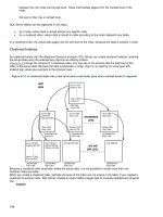
Figure 9-1
Gate Level Netlist
Synthesis.
These gate level netlists currently can be optimized for area, speed,
testability, and so on. The synthesis process is shown in Figure 9-1.
The inputs to the synthesis process are an RTL (Register Transfer
Level) VHDL description, circuit constraints and attributes for the design,
and a technology library. The synthesis process produces an optimized gate
level netlist from all of these inputs. In the next few sections, each of these
inputs is described, and we discuss the synthesis process in more detail.
Register Transfer Level
Description
A register transfer level description is characterized by a style that spec-
ifies all of the registers in a design, and the combinational logic between.
This is shown by the register and cloud diagram in Figure 9-2. The reg-
isters are described either explicitly through component instantiation or
implicitly through inference. The registers are shown as the rectangular
objects connected to the clock signal. The combinational logic is described
by logical equations, sequential control statements (CASE, IF then ELSE,
and so on), subprograms, or through concurrent statements, which are
represented by the cloud objects between registers.
233
Synthesis
Register Register
Combinational
Logic
CLK CLK
Clock
Datain Dataout
Figure 9-2
Register and Cloud
Diagram.
RTL descriptions are used for synchronous designs and describe the
clock-by-clock behavior of the design. Following is an example of an RTL
description that uses component instantiation:
ENTITY datadelay IS
PORT( clk, din, en : IN BIT;
PORT( dout : OUT BIT);
END datadelay;
ARCHITECTURE synthesis OF datadelay IS
COMPONENT dff
PORT(clk, din : IN BIT;
PORT(q,qb : OUT BIT);
END COMPONENT;
SIGNAL q1, q2, qb1, qb2 : BIT;
BEGIN
r1 : dff PORT MAP(clk, din, q1, qb1);
r2 : dff PORT MAP(clk, q1, q2, qb2);
dout <= q1 WHEN en = ‘1’ ELSE
q2;
END synthesis;
This example is the circuit for a selectable data delay circuit. The
circuit delays the input signal din by 1 or 2 clocks depending on the value
of en. If en is a 1, then input din is delayed by 1 clock. If en is a 0, input
din is delayed by 2 clocks.
Figure 9-3 shows a schematic representation of this circuit. The clock
signal connects to the clk input of both flip-flops, while the din signal
connects only to the first flip-flop. The q output of the first flip-flop is then
Chapter Nine
234
DQ
QB
CLK
EN
CLK
DIN
DOUT
Assignment Statement to
Dout
DQ
QB
CLK
r1 r2
Figure 9-3
Register Transfer
Level with Compo-
nent Instances.
connected to the d input of the next flip-flop. The selected signal assign-
ment to signal dout forms a mux operation that selects between the two
flip-flop outputs.
This example could be rewritten as follows using register inference:
ENTITY datadelay IS
PORT( clk, din, en : IN BIT;
PORT( dout : OUT BIT);
END datadelay;
ARCHITECTURE inference OF datadelay IS
SIGNAL q1, q2 : BIT;
BEGIN
reg_proc: PROCESS
BEGIN
WAIT UNTIL clk’EVENT and clk = ‘1’;
q1 <= din;
q2 <= q1;
END PROCESS;
dout <= q1 WHEN en = ‘1’ ELSE
q2;
235
Synthesis
END inference;
In the first version, the registers are instantiated using component
instantiation statements that instantiate r1 and r2.
In this version, the dff components are not instantiated, but are
inferred through the synthesis process. Register inference is discussed
more in Chapter 10, “VHDL Synthesis.” Process reg_proc has a WAIT
statement that is triggered by positive edges on the clock. When the WAIT
statement is triggered, signal q1 is assigned the value of din, and q2 is
assigned the previous value of q1. This, in effect, creates two flip-flops.
One flip-flop for signal q1, and the other for signal q2.
This is a register transfer level description because registers r1 and r2
from the first version form the registers, and the conditional signal
assignment for port dout forms the combinational logic between registers.
In the second version, the inferred registers form the register description,
while the conditional signal assignment still forms the combinational logic.
The advantage of the second description is that it is technology indepen-
dent. In the first description, actual flip-flop elements from the technol-
ogy library were instantiated, thereby making the description technology de-
pendent. If the designer should decide to change technologies, all of the
instances of the flip-flops would need to be changed to the flip-flops from
the new technology. In the second version of the design, the
designer did not specify particular technology library components, and the
synthesis tools are free to select flip-flops from whatever technology
library the designer is currently using, as long as these flip-flops match
the functionality required.
After synthesis, both of these descriptions produce a gate level descrip-
tion, as shown in Figure 9-4.
Notice that the gate level description has two registers (FDSR1) with
mux (Mux21S) logic controlling the output signal from each register. De-
pending on the technology library selected and the constraints, the mux
logic varies widely from and-or-invert gates to instantiated 2-input
multiplexers.
Following is the netlist generated by the Exemplar Logic Leonardo
Spectrum synthesis tool for the same design:
- -
Definition of datadelay
- -
- -
- -
- -
Chapter Nine
236
en
dout
MUX21S
q2
FDSR1
q1
FDSR1
dout
clk
din
CP Q
D
CP
A
Bz
S
Q
D
Figure 9-4
A Gate Level Descrip-
tion.
library IEEE, EXEMPLAR;
use IEEE.STD_LOGIC_1164.all;
use EXEMPLAR.EXEMPLAR_1164.all;
entity datadelay is
port (
clk : IN std_logic ;
din : IN std_logic ;
en : IN std_logic ;
dout : OUT std_logic) ;
end datadelay ;
architecture inference of datadelay is
component FDSR1
port (
Q : OUT std_logic ;
D : IN std_logic ;
CP : IN std_logic) ;
end component ;
component MU21S
port (
Z : OUT std_logic ;
A : IN std_logic ;
B : IN std_logic ;
S : IN std_logic) ;
end component ;
signal q2, q1: std_logic ;
begin
q2_XMPLR : FDSR1 port map ( Q=>q2, D=>q1, CP=>clk);
q1_XMPLR : FDSR1 port map ( Q=>q1, D=>din, CP=>clk);
dout_XMPLR_XMPLR : MU21S port map ( Z=>dout, A=>q2, B=>q1,
S=>en);
end inference ;
237
Synthesis
Register Register
Combinational
Logic
CLK CLK
Clock
Datain Dataout
Area = 100
Delay Constraint
Clock Constraint
Area Constraint
clock 0 10 10
max_delay 5
Figure 9-5
Register and Cloud
Diagram with Con-
straints.
The netlist matches the gate level generated schematic. The netlist con-
tains two instantiated flip-flops (FDSR1) and one instantiated 2-input mul-
tiplexer (Mux21S).
This very simple example shows how RTL synthesis can be used to
create technology-specific implementations from technology-independent
VHDL descriptions. In the next few sections, we examine much more com-
plex examples. But first, let’s look at some of the ways to control how the
synthesized design is created.
Constraints
Constraints are used to control the output of the optimization and map-
ping process. They provide goals that the optimization and mapping
processes try to meet and control the structural implementation of the
design. They represent part of the physical environment that the design
has to interface with. The constraints available in synthesis tools today
include area, timing, power, and testability constraints. In the future, we
will probably see packaging constraints, layout constraints, and so on.
Today, the most common constraints in use are timing constraints.
A block diagram of a design with some possible constraints is shown in
Figure 9-5. Again, the design is shown using the cloud notation. The com-
binational logic between registers is represented as clouds, with wires
going in and out representing the interconnection to the registers.
Chapter Nine
238
There are a number of constraints shown on the diagram including
required time constraints, late arrival constraints, and clock cycle con-
straints.
Required time constraints specify the latest time that a signal can occur.
Clock constraints are used to specify the operating frequency of the clock.
From the clock constraint, required time constraints of each signal feeding
a clocked register can be calculated. Each of these constraints is further
described in the next sections.
Timing Constraints
Typical uses for timing constraints are to specify maximum delays for
particular paths in a design. For instance, a typical timing constraint is
the required time for an output port. The timing constraint guides the
optimization and mapping to produce a netlist that meets the timing
constraint. Meeting timing is usually one of the most difficult tasks when
designing an ASIC or FPGA using synthesis tools. There may be no design
that meets the timing constraints specified. A typical delay constraint in
Leonardo synthesis format is shown here:
set_attribute -port data_out -name required_time -value 25
This constraint specifies that the maximum delay for signal data_out
should be less than or equal to 25 library units. A library unit can be
whatever the library designer used when describing the technology from
a synthesis point of view. Typically, it is nanoseconds, but can be picoseconds
or some other time measurement depending on the technology.
Clock Constraints
One method to constrain a design is to add a required_time constraint
to every flip-flop input with the value of a clock cycle. The resulting
design would be optimized to meet the one clock cycle timing constraint.
An easier method, however, is to add a clock constraint to the design. A
clock constraint effectively adds an input required_time constraint to
every flip-flop data input. An example clock constraint is shown here:
set_attribute -port clk -name clock_cycle -value 25
239
Synthesis
Register Register
Combinational
Logic
CLK CLK
Clock
Datain Dataout
drive
load
Data2
late arrival
setup/hold
Figure 9-6
Register and Cloud
Diagram with Attrib-
utes.
This example sets a clock cycle constraint on port clk with a value of
25 library units.
Some synthesis tools (such as Exemplar Logic Leonardo) do a static
timing analysis to calculate the delay for each of the nodes in the design. The
static timing analyzer uses a timing model for each element connected in
the netlist. The timing analyzer calculates the worst and best case timing
for each node by adding the contribution of each cell that it traverses.
The circuit is checked to see if all delay constraints have been met. If
so, the optimization and mapping process is done; otherwise, alternate
optimization strategies may be applied
—
such as adding more parallelism
or more buffered outputs to the slow paths
—
and the timing analysis is
executed again. More detail about the typical timing analysis is discussed
later in the section “Technology Libraries.”
Attributes
Attributes are used to specify the design environment. For instance,
attributes specify the loading that output devices have to drive, the drive
capability of devices driving the design, and timing of input signals. All
of this information is taken into account by the static timing analyzer to
calculate the timing through the circuit paths. A cloud diagram showing
attributes is shown in Figure 9-6.
Chapter Nine
240
Load
Each output can specify a drive capability that determines how many
loads can be driven within a particular time. Each input can have a load
value specified that determines how much it will slow a particular driver.
Signals that are arriving later than the clock can have an attribute that
specifies this fact.
The Load attribute specifies how much capacitive load exists on a
particular output signal. This load value is specified in the units of the
technology library in terms of pico-farads, or standard loads, and so on.
For instance, the timing analyzer calculates a long delay for a weak driver
and a large capacitive load, and a short delay for a strong driver and a
small load. An example of a load specification in Leonardo synthesis format
is shown here:
set_attribute -port xbus -name input_load -value 5
This attribute specifies that signal xbus will load the driver of this
signal with 5 library units of load.
Drive
The Drive attribute specifies the resistance of the driver, which controls
how much current it can source. This attribute also is specified in the units
of the technology library. The larger a driver is the faster a particular path
will be, but a larger driver takes more area, so the designer needs to trade
off speed and area for the best possible implementation. An example of a
drive specification in Leonardo synthesis format is shown here:
set_attribute -port ybus -name output_drive -value 2.7
This attribute specifies that signal ybus has 2.7 library units of drive
capability.
Arrival Time
Some synthesis tools (such as Exemplar Logic Leonardo) use a static
timing analyzer during the synthesis process to check that the logic being
created matches the timing constraints the user has specified. Setting the
arrival time on a particular node specifies to the static timing analyzer
241
Synthesis
when a particular signal will occur at a node. This is especially important
for late arriving signals. Late arriving signals drive inputs to the current
block at a later time, but the results of the current block still must meet
its own timing constraints on its outputs. Therefore, the path to the output
of the late arriving input must be faster than any other inputs, or the
timing constraints of the current block cannot be met.
Technology Libraries
Technology libraries hold all of the information necessary for a synthesis
tool to create a netlist for a design based on the desired logical behavior,
and constraints on the design. Technology libraries contain all of the
information that allows the synthesis process to make the correct choices
to build a design. Technology libraries contain not only the logical func-
tion of an ASIC cell, but the area of the cell, the input to output timing of
the cell, any constraints on fanout of the cell, and the timing checks that
are required for the cell. Other information stored in the technology
library may be the graphical symbol of the cell for use in schematics.
Following is an example technology library description of a 2-input
AND gate written in Synopsys .lib format:
library (xyz) {
cell (and2) {
area : 5;
pin (a1, a2) {
direction : input;
capacitance : 1;
}
pin (o1) {
direction : output;
function : “a1 * a2”;
timing () {
intrinsic_rise : 0.37;
intrinsic_fall : 0.56;
rise_resistance : 0.1234;
fall_resistance : 0.4567;
related_pin : “a1 a2”;
}
}
}
}
This technology library describes a library named xyz with one library
cell contained in it. The cell is named and2 and has two input pins a1 and
Chapter Nine
242
a2 and one output pin o1. The cell requires 5 units of area, and the input
pins have 1 unit of loading capacitance to the driver driving them. The
intrinsic rise and fall delays listed with pin o1 specify the delay to the
output with no loading. The timing analyzer uses the intrinsic delays plus
the rise and fall resistance with the output loading to calculate the delay
through a particular gate. Notice that the function of pin o1 is listed as
the AND of pins a1 and a2. Also, notice that pin o1 is related to pins a1 and
a2 in that the timing delay through the device is calculated from pins a1
and a2 to pin o1.
Most synthesis tools have fairly complicated delay models to calculate
timing through an ASIC cell. These models include not only intrinsic rise
and fall time, but output loading, input slope delay, and estimated wire
delay. A diagram illustrating this is shown in Figure 9-7.
The total delay from gate A1 to gate C1 is:
intrinsic_delay + loading_delay + wire_delay + slope_delay
The intrinsic delay is the delay of the gate without any loading. The
loading delay is the delay due to the input capacitance of the gate being
driven. The wire delay is an estimated delay used to model the delay
through a typical wire used to connect cells together. It can be a statistical
model of the wire delays usually based on the size of the chip die. Given
a particular die size, the wire loading effect can be calculated and added
to the overall delay. The final component in the delay equation is the
extra delay needed to handle the case of slowly rising input signals due
to heavy loading or light drive.
Slope Delay
Intrinsic
Delay
Loading
Delay
Wire Delay
A1
B1
C1
Figure 9-7
Delay Effects Used in
Delay Model.
243
Synthesis
In the preceding technology library, the intrinsic delays are given in the
cell description. The loading delay is calculated based on the load applied
to the output pin o1 and the resistance values in the cell description. The
value calculated for the wire delay depends on the die size selected by the
user. Selecting a wire model scales the delay values. Finally, the input
slope delay is calculated by the size of the driver, in this example, A1, and
the capacitance of the gate being driven. The capacitance of the gate
being driven is in the technology library description.
Technology libraries can also contain data about how to scale delay
information with respect to process parameters and operating conditions.
Operating conditions are the device operating temperature and power
supply voltage applied to the device.
Synthesis
To convert the RTL description to gates, three steps typically occur. First,
the RTL description is translated to an unoptimized boolean description
usually consisting of primitive gates such as AND and OR gates, flip-flops,
and latches. This is a functionally correct but completely unoptimized
description. Next, boolean optimization algorithms are executed on this
boolean equivalent description to produce an optimized boolean equivalent
description. Finally, this optimized boolean equivalent description is
mapped to actual logic gates by making use of a technology library of the
target process. This is shown in Figure 9-8.
Translation
The translation from RTL description to boolean equivalent description
is usually not user controllable. The intermediate form that is generated
is usually a format that is optimized for a particular tool and may not
even be viewable by the user.
All IF, CASE, and LOOP statements, conditional signal assignments, and
selected signal assignment statements are converted to their boolean
equivalent in this intermediate form. Flip-flops and latches can either be
instantiated or inferred; both cases produce the same flip-flop or latch
entry in the intermediate description.
Chapter Nine
244
Created by
User
Translate
Optimize
Map to Gates
VHDL RTL
Description
Unoptimized Boolean
Description
Optimized Boolean
Description
Gate Level
Netlist
Figure 9-8
Synthesis Process.
Boolean Optimization
The optimization process takes an unoptimized boolean description and
converts it to an optimized boolean description. In many designers’ eyes,
this is where the real work of synthesis gets done. The optimization
process uses a number of algorithms and rules to convert the unoptimized
boolean description to an optimized one. One technique is to convert the
unoptimized boolean description to a very low-level description (a pla
format), optimize that description (using pla optimization techniques),
245
Synthesis
and then try to reduce the logic generated by sharing common terms (in-
troducing intermediate variables).
Flattening
The process of converting the unoptimized boolean description to a pla
format is known as flattening, because it creates a flat signal represen-
tation of only two levels: an AND level and an OR level. The idea is to get
the unoptimized boolean description into a format in which optimization
algorithms can be used to optimize the logic. A pla structure is a very easy
description in which to perform boolean optimization, because it has a
simple structure and the algorithms are well known. An example of a
boolean description is shown here:
Original equations
a = b and c;
b = x or (y and z);
c = q or w;
This description shows an output a that has three equations describing
its function. These equations use two intermediate variables b and c to
hold temporary values which are then used to calculate the final value
for a. These equations describe a particular structure of the design that
contains two intermediate nodes or signals, b and c. The flattening
process removes these intermediate nodes to produce a completely flat
design, with no intermediate nodes. For example, after removing inter-
mediate variables:
a = (x and q) or (q and y and z) or (w and x) or (w and y
and z);
This second description is the boolean equivalent of the first, but it has
no intermediate nodes. This design contains only two levels of logic gates:
an AND plane and an OR plane. This should result in a very fast design
because there are very few logic levels from the input to the output. In
fact, the design is usually very fast. There are, however, a number of prob-
lems with this type of design.
First, this type of design can actually be slower than one that has more
logic levels. The reason is that this type of design can have a tremendous
fanout loading on the input signals because inputs fan out to every term.
Second, this type of design can be very large, because there is no sharing
between terms. Every term has to calculate its own functionality. Also,
Chapter Nine
246
there are a number of circuits that are difficult to flatten, because the
number of terms created is extremely large. An equation that only con-
tains AND functions produces one term. A function that contains a large
XOR function can produce hundreds or even thousands of terms. A 2-input
XOR has the terms A and (not B) or B and (not A). An N-input XOR has
2**(N-1) terms. For instance, a 16-input XOR has 32,768 terms and a 32-
bit XOR has over 2 billion terms. Clearly, designs with these types of func-
tions cannot be flattened.
Flattening gets rid of all of the implied structure of design whether it
is good or not. Flattening works best with small pieces of random control
logic that the designer wants to minimize. Used in conjunction with struc-
turing, a minimal logic description can be generated.
Usually, the designer wants a design that is nearly as fast as the flat-
tened design, but is much smaller in area. To reduce the fanout of the
input pins, terms are shared. Some synthesis vendors call this process
structuring or factoring.
Factoring
Factoring is the process of adding intermediate terms to add structure to a
description. It is the opposite of the flattening process. Factoring is usually
desirable because, as was mentioned in the last section, flattened designs
are usually very big and may be slower than a factored design because of
the amount of fanouts generated. Following is a design before factoring:
x = a and b or a and d;
y = z or b or d;
After factoring the common term, (b or d), is factored out to a separate
intermediate node. The results are shown here:
x = a and q;
y = z or q;
q = b or d;
Factoring usually produces a better design but can be very design-
dependent. Adding structure adds levels of logic between the inputs and
outputs. Adding levels of logic adds more delay. The net result is a smaller
design, but a slower design. Typically, the designer wants a design that is
nearly as fast as the flattened design if it was driven by large drivers, but
as small as the completely factored design. The ideal case is one in which
247
Synthesis
the critical path was flattened for speed and the rest of the design was
factored for small area and low fanout.
After the design has been optimized at the boolean level, it can be
mapped to the gate functions in a technology library.
Mapping to Gates
The mapping process takes the logically optimized boolean description
created by the optimization step and uses the logical and timing infor-
mation from a technology library to build a netlist. This netlist is targeted
to the user’s needs for area and speed. There are a number of possible
netlists that are functionally the same but vary widely in speed and area.
Some netlists are very fast but take a lot of library cells to implement, and
others take a small number of library cells to implement but are very slow.
To illustrate this point, let’s look at a couple of netlists that implement
the same functionality. Following is the VHDL description:
LIBRARY IEEE;
USE IEEE.std_logic_1164.ALL;
USE IEEE.std_logic_unsigned.ALL;
ENTITY adder IS
PORT( a,b : IN std_logic_vector(7 DOWNTO 0);
PORT( c : OUT std_logic_vector(7 DOWNTO 0)
PORT( );
END adder;
ARCHITECTURE test OF adder IS
BEGIN
c <= a + b;
END test;
Both of the examples implement an 8-bit adder, but the first imple-
mentation is a small but slower design, and the second is a bigger but fast
design. The small but slower design is an 8-bit ripple carry adder shown
in Figure 9-9. The bigger but faster design is an 8-bit lookahead adder
shown in Figure 9-10.
Both of these netlists implement the same function, an 8-bit adder. The
ripple carry adder takes less cells to implement but is a slower design
because it has more logic levels. The lookahead adder takes more cells to
implement but is a faster design because more of the boolean operations are
calculated in parallel. The additional logic to calculate the functionality
in parallel adds extra logic to the design making the design bigger.
Figure 9-9
Smaller but Slower 8-Bit Ripple Carry Adder.
248
249
Figure 9-10
Bigger but Faster 8-Bit Lookahead Adder.
Chapter Nine
250
In most synthesis tools, the designer has control over which type of
adder is selected through the use of constraints. If the designer wants to
constrain the design to a very small area and doesn’t need the fastest
possible speed, then the ripple carry adder probably works. If the designer
wants the design to be as fast as possible and doesn’t care as much about
how big the design gets, then the lookahead adder is the one to select.
The mapping process takes as input the optimized boolean description,
the technology library, and the user constraints, and generates an opti-
mized netlist built entirely from cells in the technology library. During the
mapping process, cells are inserted that implement the boolean function
from the optimized boolean description. These cells are then locally opti-
mized to meet speed and area requirements. As a final step, the synthesis
tool has to make sure that the output does not violate any of the rules of
the technology being used to implement the design, such as the maximum
number of fanouts a particular cell can have.
SUMMARY
In this chapter, we discussed some of the basic principles of the synthesis
process. In the next chapter, we take a closer look at how to write models
that can be synthesized.
CHAPTER
10
VHDL Synthesis
In this chapter, we focus on how to write VHDL that can
be read by synthesis tools. We start out with some simple
combinational logic examples, move on to some sequential
models, and end the chapter with a state machine de-
scription.
All of the examples are synthesized with the Exemplar
Logic Leonardo synthesis environment. The technology li-
brary used is an example library from Exemplar Logic. All
of the output data should be treated as purely sample out-
puts and not representative of how well the Exemplar
Logic tools work with real design data and real con-
straints.
10
Chapter Ten
252
c
a
d
b
out
out
in [1]
in [0]
in [1]
in [0]
Figure 10-1
Model
Implementation.
Simple Gate
—
Concurrent
Assignment
The first example is a simple description for a 3-input OR gate:
LIBRARY IEEE;
USE IEEE.std_logic_1164.ALL;
ENTITY or3 IS
PORT (a, b, c : IN std_logic;
PORT (d : OUT std_logic);
END or3;
ARCHITECTURE synth OF or3 IS
BEGIN
d <= a OR b OR c;
END synth;
This model uses a simple concurrent assignment statement to describe
the functionality of the OR gate. The model specifies the functionality
required for this entity, but not the implementation. The synthesis tool
can choose to implement this functionality in a number of ways, depending
on the cells available in the technology library and the constraints on
the model. For instance, the most obvious implementation is shown in
Figure 10-1.
This implementation uses a 3-input OR gate to implement the func-
tionality specified in the concurrent signal assignment statement contained
in architecture synth.
What if the technology library did not contain a 3-input OR device? Two
other possible implementations are shown in Figures 10-2 and 10-3.
The first implementation uses a 3-input NOR gate followed by an inverter.
The synthesis tool may choose this implementation if there are no 3-input
OR devices in the technology library. Alternatively, if there are no 3-
input devices, or if the 3-input devices violate a speed constraint, the
253
VHDL Synthesis
b
c
a
PAD
PAD
PAD
INBUF
INBUF
INBUF
Y
YYD
Y
A
B
C
OUTBUF
PAD
d
NANDOC
Figure 10-2
3-Input OR.
3-input OR function could be built from four devices, as shown in Figure
10-3. Given a technology library of parts, the functionality desired, and
design constraints, the synthesis tool is free to choose among any of the
implementations that satisfy all the requirements of a design, if such a
design exists. There are lots of cases where the technology or constraints
are such that no design can meet all of the design requirements.
IF Control Flow Statements
In the next example, control flow statements such as IF THEN ELSE are
used to demonstrate how synthesis from a higher level description is
accomplished. This example forms the control logic for a household alarm
system. It uses sensor input from a number of sensors to determine
whether or not to trigger different types of alarms. Following is the input
description:
LIBRARY IEEE;
USE IEEE.std_logic_1164.ALL;
ENTITY alarm_cntrl IS
PORT( smoke, front_door, back_door, side_door,
PORT( alarm_disable, main_disable,
PORT( water_detect : IN std_logic;
PORT( fire_alarm, burg_alarm,
PORT( water_alarm : OUT std_logic);
END alarm_cntrl;
ARCHITECTURE synth OF alarm_cntrl IS
BEGIN
PROCESS(smoke, front_door, back_door, side_door,
PROCESS(alarm_disable, main_disable,
PROCESS(water_detect)
BEGIN
Chapter Ten
254
c
a
d
b
out
out
in [1]
in [0]
in [1]
in [0]
Figure 10-3
Another 3-Input OR
Implementation.
IF ((smoke = ‘1’) AND (main_disable = ‘0’)) THEN
fire_alarm <= ‘1’;
ELSE
fire_alarm <= ‘0’;
END IF;
IF (((front_door = ‘1’) OR (back_door = ‘1’) OR
(side_door = ‘1’)) AND
((alarm_disable = ‘0’) AND (main_disable =
‘0’))) THEN
burg_alarm <= ‘1’;
ELSE
burg_alarm <= ‘0’;
END IF;
IF ((water_detect = ‘1’) AND (main_disable = ‘0’))
THEN
water_alarm <= ‘1’;
ELSE
water_alarm <= ‘0’;
END IF;
END PROCESS;
END synth;
The input description contains a number of sensor input ports such as
a smoke detector input, a number of door switch inputs, a basement water
detector, and two disable signals. The main_disable port is used to disable
all alarms, while the alarm_disable port is used to disable only the
burglar alarm system.
The functionality is described by three separate IF statements. Each
IF statement describes the functionality of one or more output ports. No-
tice that the functionality could also be described very easily with equa-
tions, as in the first example. Sometimes, however, the
IF statement style
is more readable. For instance, the first
IF statement can be described by
the following equation:
255
VHDL Synthesis
back_door
burg_alarm
fire_alarm
water_alarm
side_door
front_door
smoke
main_disable
water_detect
alarm_disable
NOR2A
D0
D1
D2
D3
S00
S01
S10
S11
NOR2A
CM8
Y
Y
GND
Y
VCC
AY
Y
Y
AY
A
A
B
B
Figure 10-4
A sample synthesized
output.
fire_alarm <= smoke and not(main_disable);
Because the three IF statements are separate and they generate
separate outputs, we can expect that the resulting logic would be three sep-
arate pieces of logic. However, the main_disable signal is shared between
the three pieces of logic. Any operations that make use of this signal may
be shared by the other logic pieces. How this sharing takes place is deter-
mined by the synthesis tool and is based on the logical functionality of the
design and the constraints. Speed constraints may force the logical oper-
ations to be performed in parallel.
A sample synthesized output is shown in Figure 10-4. Notice that
signal main_disable connects to all three output gates, while signal
alarm_disable only connects to the alarm control logic. The logic for
the water alarm and smoke detector turn out to be quite simple, but we
could have guessed that because our equations were so simple. The next
example is not so simple.
Chapter Ten
256
Case Control Flow Statements
The next example is an implementation of a comparator. There are two 8-
bit inputs to be compared and a CTRL input that determines the type of
comparison made. The possible comparison types are A > B, A < B, A ϭ B,
A ≠ B, A м B, and A Ϲ B. The design contains one output port for each of
the comparison types. If the desired comparison output is true, then the out-
put value on that output port is a ‘1’. If false, the output port value is a
‘0’. Following is a synthesizable VHDL description of the comparator:
PACKAGE comp_pack IS
TYPE bit8 is range 0 TO 255;
TYPE t_comp IS (greater_than, less_than, equal,
not_equal, grt_equal, less_equal);
END comp_pack;
LIBRARY IEEE;
USE IEEE.std_logic_1164.ALL;
USE WORK.comp_pack.ALL;
ENTITY compare IS
PORT( a, b : IN bit8;
PORT( ctrl : IN t_comp;
PORT( gt, lt, eq, neq, gte, lte : OUT std_logic);
END compare;
ARCHITECTURE synth OF compare IS
BEGIN
PROCESS(a, b, ctrl)
BEGIN
gt <= ‘0’; lt <= ‘0’; eq <= ‘0’; neq <= ‘0’; gte <=
‘0’; lte <= ‘0’;
CASE ctrl IS
WHEN greater_than =>
IF (a > b) THEN
gt <= ‘1’;
END IF;
WHEN less_than =>
IF (a < b) THEN
lt <= ‘1’;
END IF;
WHEN equal =>
IF (a = b) THEN
eq <= ‘1’;
END IF;
WHEN not_equal =>
IF (a /= b) THEN
neq <= ‘1’;
END IF;
WHEN grt_equal =>
IF (a >= b) THEN