MANAGING POWER ELECTRONICS VLSl and DSP-Driven Computer Systems phần 2 pptx
Bạn đang xem bản rút gọn của tài liệu. Xem và tải ngay bản đầy đủ của tài liệu tại đây (1.81 MB, 41 trang )
20
Chapter
2
Power
Management Technologies
2.3
Discrete
Power
Technology: Processing and
Packaging
Microprocessors for PCs are at the forefront of the computing industry,
leading with huge nano-scale chips built
in
multi billion dollar fabrication
plants.
So
far, the success
of
the semiconductor industry has been assured
by Moore’s law-a concept that underscores the fast-paced dynamic of the
industry. However, new chips
in
smaller footprints are upping the trend for
increasing power densities to amazing levels. At every new technology
juncture, the CPU becomes denser and hotter. Keeping pace with changing
densities, compounded with the need for disposing the resulting heat, is
creating more challenges for applications designers.
Providing power from the AC line is also becoming an issue for
designers. The number and growth rate
of
electronic appliances is driving
a huge demand for power, prompting concerns for power distribution and
energy conservation and spurring a slew of protocols and initiatives aimed
at minimizing the waste of power. These requirements are pushing tech-
nology advancements beyond the traditional cost-oriented model of mini-
mizing the appliance’s Bill of Materials
(BOM)
to look for new solutions.
At the core of all power management solutions, from the wall
to
the
board, are power transistors. The evolution of discrete semiconductors is
essential for supporting Moore’s law, and thereby maintaining the indus-
try’s healthy growth. Not surprisingly, designing and mass producing cost-
effective discrete transistors capable of efficiently handling power requires
increasingly sophisticated semiconductor processes and packaging.
From Wall
to
Board
Electric power is transferred to the CPU in two crucial steps: from the high
voltage AC line to an intermediate DC voltage and from there to the low
voltage regulator
(VR),
which is needed
to
power the CPU. The high volt-
age “planar technology” transistor underlying this AC-DC conversion
must sustain voltages
in
the
600-700
V
range and few Amperes of current;
meanwhile, the low voltage “trench” transistor powering the CPU has to
handle a few volts with hundreds
of
Amperes. Both conversions have to be
accomplished with the lowest possible power losses. It stands to reason,
then, that such diverse performance requirements are satisfied by two quite
different discrete MOSFET transistor technologies, “planar” for high volt-
age and “trench” for low voltage.
Discrete Power Technology: Processing and Packaging
21
Power MOSFET Technology
Basics
Conduction
Losses
Power MOSFET technologies comprise
a
number of key elements that
impact on-state, or conduction losses. These elements include
a
substrate
to
provide mechanical stability,
a
region used for blocking the drain poten-
tial
in
the off-state, and the conduction channel that provides gate control.
The greatest penalty of on-resistance for high voltage power MOS-
FETs is found
in
the epitaxial region. For conventional high voltage
devices, the construction requires thick, highly resistive epitaxial material
to
support the
600
V
blocking requirement. For devices below approxi-
mately 200
V,
this region becomes less significant. Advanced high voltage
devices utilize
a
technique called “charge balance” which is used
to
reduce
conduction loss
in
the epitaxial region.
With power MOSFETs, the conduction channel resistance is deter-
mined by the channel length, the distance through which carriers must
flow, and channel width, is the amount
of
transistor channel that is con-
structed in parallel. Lower resistance is achieved by increasing the channel
width for a given silicon area. Due to the low conduction losses in the epi-
taxial region of low voltage devices, the channel density is critical for
reducing conduction losses.
Switching Losses
The channel construction technique
has
a
significant impact on the switch-
ing performance of
a
power MOSFET. The amount of polysilicon gate
area that overlaps with the epitaxial region, the
N+
source diffusions, and
the source metal are key design parameters. This area,
in
conjunction with
the thickness of the dielectric materials between these regions, sets para-
sitic capacitances that must be charged and discharged during each switch-
ing event.
Planar Power
MOSFET
Technology
The best choice for channel construction for high voltage power MOSFET
devices is planar construction,
as
shown in Figure 2-12. In this type
of
construction, the polysilicon and the channel are displaced on the horizon-
tal silicon surface of
a
planar device. Due
to
the conduction losses in the
epitaxial region
of
high voltage devices, there would be
a
minimal benefit
of
a
high channel density construction. In addition, low capacitances of the
planar channel provide low switching losses. Planar construction, when
combined with the charge balance epitaxial structure, provides optimized
performance of
a
high voltage power MOSFET.
22
Chapter
2
Power Management Technologies
Figure
2-1 2
Planar DMOS transistor cross-section.
An example
of
this type
of
planar MOSFET technology is the
FCPl1
N60
SuperFETTM from Fairchild Semiconductor. This product typ-
ifies a new generation of high voltage MOSFET that offers very low on-
resistance and low gate charge performance. It does this using proprietary
technology utilizing the advanced charge balance technique. Such
advanced technology is tailored
to
minimize conduction loss, provide
superior switching performance, and withstand extreme dv/dt rate and
higher avalanche energy. Consequently, this kind of device is very well
suited for various AC-DC power conversion designs using switching mode
operation when system miniaturization and higher efficiency is needed.
The future holds ongoing improvements in this type
of
technology for bet-
ter conduction and switching loss performance.
Power Trench
MOSFET
Technology
For a low voltage power MOSFET device, channel conduction is best con-
structed utilizing a trench channel structure, which is illustrated
in
Figure
2-1
3.
This construction technique places the polysilicon and chan-
nel vertically in the silicon epitaxial region. As a result, the channel den-
sity is maximized, providing a significant conduction reduction when
compared to a planar device. In addition, low conduction losses per unit
area allow the chip size to be reduced, improving switching losses. Also,
capacitances are reduced through a careful tailoring
of
the capacitor
dielectric thicknesses. This combination of low resistance and low
switching losses of power trench MOSFETs provides the optimal solution
for powering the CPU.
Discrete Power Technology: Processing and Packaging
23
Figure
2-1
3
Trench MOSFET (channel structure).
An example of this technique is the delivery
of
74 A continuous (93 A
peak) without heatsink to Prescott class CPUs using a three-phase buck
converter that utilizes planar DMOS discrete transistors in the power
stage. In this example the
buck
converter
utilizes devices such as Fair-
child’s FDD6296 high side MOSFET DPAK (one per phase) and a
FDD8896 low side MOSFET DPAK (two per phase), in combination with
a FANS019 PWM controller (one) and a FANS009 driver (one per phase).
Ongoing changes to these technologies will further enhance both the
conduction and switching performance
of
the existing trench MOSFETs.
As a result, the improvements will deliver increasingly better performance.
Pa
c
ka
g
e
Techno
I
og
i
es
Today, much work is being done to develop low parasitic (i.e., ohmic resis-
tance, wire inductance) packages.
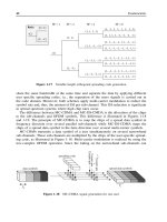
Figure 2-14 shows a power Ball Grid Array (BGA) package capable
of delivering unprecedented levels of power thanks to the substitution
of
the wire bonds solder balls. A surrounding drain frame structure, which
dramatically reduces the package resistance and inductance parasitics, is
another important benefit
of
BGA packaging.
For example, in a server application, one BGA-packaged FDZ7064S
device on the high side, and two FDZS047N on the low side, can deliver
40 Nphase with a power density of
50
W/in2. Hence, a four-phase imple-
mentation can easily deliver 200 A to the CPU.
24
Chapter
2
Power Management Technologies
Figure
2-14
Illustration of a power BGA package.
2.4
Ongoing Trends
As wall-to-board power challenges will continue to escalate,
MOSFET
transistor processing and packaging solutions will continue evolving. A
system approach to power distribution will assure the best mix
of
pro-
cesses and package technologies for the powering
of
modern appliances.
At the motherboard level
(DC-DC
conversion), the need
to
efficiently dis-
pose of the heat in increasingly smaller spaces will continue to drive the
need for trench and package technology that offers lower and lower para-
sitics. At the
silver
box
level (AC-DC conversion), the need
to
draw effi-
cient power from the AC line will drive future offline architectures toward
the use
of
more planar discrete transistors of increased sophistication
in
order to support existing and new features like
Power Factor Correction
(PFC)
with fewer overall power losses.
Modern circuit design is a “mixed signal” endeavor thanks to the availabil-
ity
of sophisticated process technologies that make available bipolar and
CMOS, power and signal, and passive and active components on the same
die. It is then up to the circuit designer’s creativity and inclination to assem-
ble these components into the analog and/or logic building blocks necessary
to develop the intended system on a chip. While the digitalization of tradi-
tional analog blocks continues, new analog blocks are invented all the time.
Examples of new analog functions are charge-pump voltage regulators,
MOSFETs, and LED drivers.
A
contemporary example of digital technol-
ogy cutting deep into analog core functions is the digitalization of the fre-
quency compensation
in
the control loop of switching regulators. In this
case while the feat has been accomplished-and it can indeed be exhilarat-
ing to move
poles
and
zeros
(see
glossary)
around with a mouse click-it is
not clear that the feature of digital frequency compensation, and its associ-
ated cost in silicon, is always justified.
So
while digital technology circuits
and processes4ontinues to gain ground, analog keeps reinventing itself
and rebuilding around a central analog core of functions that is tough to
crack. We don’t expect to see the digitalization
of
an analog circuit like the
band-gap voltage reference-namely a digital circuit taking the place of the
current analog one-happening any time soon. In this section we will dis-
cuss a number of analog, digital, bipolar, and CMOS circuits. It would be
hopeless to
try
to report systematically all the building blocks for mixed-sig-
nal circuit design, or even just the main ones. Instead we will adopt the tech-
nique of “build as you
go.”
With this
in
mind we will
start
from the single
transistor and build up to some complex functions like linear and switching
regulators that
are
at the core of power conversion and management.
25
26
ChaDter
3
Circuits
Part
I
Analog
Circuits
3.1
In this section we will discuss some fundamental analog building blocks
for power management. We will review quickly the main properties of the
elementary components, the transistors,
so
that we can use them to build
elementary circuits like current mirrors and buffer stages. We will then use
these elements and circuits to generate the analog building blocks like
operational amplifiers and voltage references. Finally we will combine
these analog building blocks into functional circuits. Given the subject of
this book, not surprisingly, the functions we are interested in are voltage
regulators, which are at the center of power distribution and management.
The process of assembling elementary electrical components into a
fully
functional electronic product-namely the system design of an electronic
product-can all be implemented
on
a
single die, leading
to
a monolithic
single integrated circuit, or can be spread over many chips, for example
a
discrete power transistor chip and a controller IC assembled
in
a module.
Modern circuit design, both at the discrete and IC levels, relies
on
a mix of
bipolar and CMOS elements. Power management integrated circuits can
now be built
on
mixed bipolar CMOS and DMOS processes if the level of
performance and complexity justifies it. System design will mix and
match such ICs with external discrete components that will again range
from bipolar
to
CMOS and DMOS with the selection generally being
driven by cost first and performance second.
In
the rest
of
this section we often draw bipolar circuits, but every cir-
cuit discussed has its counterpart in CMOS. By substituting the NPN with
its CMOS dual, the N-channel MOS transistor, and the PNP with its dual,
the P-channel MOS, all the functions discussed
in
bipolar can be repli-
cated in CMOS.
Transistors
The NPN transistor (Figure
3-1)
is the king of the traditional bipolar ana-
log integrated circuits world. In fact in the most basic and most cost
effective analog IC processes, the chip designer has at its disposal just that;
a good NPN transistor. The rest, PNPs, resistors and capacitors are just by-
products, a notch better than parasites.
For
intuitive, back-of-the-envelope
type analysis, it is sufficient to model the transistor mostly in DC, keeping
in mind that the bandwidth of such an element is finite. When complexity,
like small-signal AC behavior, is added to the model, computing simula-
Transistors
27
C
C
P
E
rE
=
VT/lE
5
+
Figure
3-1
NPN
Transistor
(a)
symbol and (b) model.
tions should be used since the math quickly becomes hopeless. In
Figure 3-1 the
NPN
transistor is shown with its symbol
(a)
and its
DC
model (b). In this component, the current flow enters the collector and
base and exits through
the
emitter. Simply stated, the transistor conducts
a
collector current
I,
which is
a
copy
of
the base current
IB
amplified by
a
factor
of
beta
(p).
It follows that the emitter current
IE
is one plus beta
times the base current.
A
typical value for the amplification factor is
100.
NPNs
have excellent dynamic performance, or bandwidth, measured by
their cutoff frequency
(fT);
easily above
1
GHz.
The
PNP
transistor (Figure 3-2) is complementary to the
NPN,
with the
current flow entering the emitter and exiting the collector and base, the
opposite of what happens in the
NPN.
Simplicity dictates that
PNPs
are a
by-product
of
the
NPN
construction; hence they often have less beta cur-
rent gain and are slower than
NPNs.
A
typical value for their amplification
factor is
50
and their cutoff frequency
(fT),
is generally above
1
MHz.
Tra
ns-Co
n
d
ucta
n
ce
In addition to current gain, and bandwidthfp another important element of
the transistor model is its trans-conductance gain
GM,
namely the amount
of current
in
the emitter
as
a
result of
a
voltage input in the base-emitter
junction. The small signal transistor model in Figures 3-1 and 3-2 shows
28
Chapter
3
Circuits
E
P
E
Figure
3-2
PNP
Transistor (a) symbol and (b) model.
that the base-emitter voltage
of
a transistordhe infamous
0.7
V roughly
constant voltage-is modulated by the resistance
rE
where
rE
=
VgIE
Eq.
3-1
V,
=
KT/q
=
26 mV at ambient temperature
of
25°C
Eq.
3-2
where
K
is the Boltzman constant,
T
is the temperature
in
degrees Kelvin,
and
q
is equal to the electron charge in Coulombs.
It follows then that a small signal voltage
AV
applied at the transistor
base-emitter junction will act solely
on
the resistor
rE
and develop a corre-
sponding current
dl.
Therefore, the trans-conductance gain
G,
is the exact inverse
of
rE.
Since we deal more easily with resistors than trans-conductors, we will
continue to represent the trans-conductance gain with the resistor
rE
explicitly drawn in the model or simply implied in the transistor symbol.
Tr a
n
s
is
t
o
r as Tra
ns
f
e
r-
R
e
s
i
s
t
or
A transistor with 1 mA of emitter current will exhibit an emitter resistance
of 26 mV/1
mA
or 26
R
according to Eq. 3-1. This, as any resistance
in
an
emitter, produces an amplified resistance as seen from the base.
In
fact
staying with this numeric example, an emitter current
of
1
mA, in addition
to a
26
mV drop in the emitter-base voltage, will produce a base current
Transistors
29
variation
of
approximately
10
pA
(1
mA divided by an amplification of
a
+
1
or
101).
From the base vantage point
a
26 mV fluctuation in
response
to
a
base current fluctuation
of
10
pA is interpreted
as
a
resis-
tance
of
26 mV/10 pA
=
2.6
kL2
Naturally such transfer of resistance from
low
in
the emitter to high in the base is the property that gives the name
transistor or, transfer resistor to the electrical component.
Transistor Equations
The voltage
to
current relation in
a
bipolar transistor follows
a
logarithmic
law given by
VBE
=
VT
x
In(l/lo) Eq.
3-4
where
VT
is the thermal voltage and
lo
is
a
characteristic current that
depends
on
the specific process. This has some pretty interesting implica-
tions; for example, if the transistor from
Eq.
34 carries
a
current
x
times
higher, we can write
VBE'
=
VT
x
ln(x
x
1/10)
Eq.
3-5
The increase in voltage from the factor
of
x
increase in current will be
dVBE
=
VBE'
-
VBE
=
VT
x
In
(x)
=
(kT/q)ln(x) Eq.
3-6
Given that
V,
=
26 mV at ambient temperature, we see easily that
doubling the current in
a
transistor
(x
=
2)
will raise its
VBE
by
18
mV
(say
from 700 mV to 718 mV) and
a
10x increase in current will raise the
VBE
by 60 mV. In gross approximation we can consider the
VBE
of
a
transistor
constant around 0.7 V, but to be more precise the
VBE
shifts logarithmi-
cally with the current.
The relative insensitivity of the transistor
VBE
to current variations
is
exploited
in
building current sources and voltage references.
Naturally the opposite is true for the current variation
as
a
function
of
voltage. In fact if we invert the previous equation we have
I
=
lo
x
exp(
VBElVT)
Eq. 3-7
which shows that the current varies exponentially with the
VBE.
We
already know that
a
variation
of
18 mV
on
the
VBE
will double the current
in
the transistor. For
a
quick estimate of variations in current due to small
voltage variations, we can linearize the exponential law and find that the
30
Chapter
3
Circuits
current will vary at roughly two percent per millivolt. This strong depen-
dence of current on the
VBE
explains why the transistor is normally driven
with current, not voltage.
This also explains how difficult it is to deal with offsets, or small volt-
age variations between identical transistors. Two identical transistors
biased at the same identical voltage will have their current mismatched
with a two percent error if their
VBE
differs by just
1
mV.
MOS
versus Bipolar Transistors
The dual of bipolar NPN and PNP transistors in CMOS technology are the
P-channel and N-channel MOS transistors in Figure
3-3.
The general
function of the transistors are the same independently as their implementa-
tion but there are pros and cons to using both technologies. Generally
speaking, the base, the emitter, and the collector in the bipolar transistor
are analogous
to
the gate, source and drain in the MOS transistor, respec-
tively. The bipolar transistors' main problem, which
is
not present in
CMOS,
is their need for a base current in order to function. Such current is
a net transfer
loss
from emitter to collector. While the base current is small
in
small signal operation, in power applications, where the transistor is
used as a switch, the base current necessary to keep the transistor on can
be very high. This high base current can lead to implementations with very
poor efficiency. With the popularity of portable electronics and the need to
extend battery life,
it
is
no
wonder that CMOS
often
tends to have the
upper hand over bipolar technologies. The advantage of bipolar over
CMOS is that it has better trans-conductance gain and better matching,
leading to better differential input gain stages and better voltage refer-
ences. The best performance processes are mixed-mode Bipolar and
CMOS (BiCMOS) or Bipolar, CMOS, and DMOS (BCD) processes in
which the designer can use the best component for the task at hand.
G+
4
-7
di
r'
Figure
3-3
(a) N-channel MOS transistor and (b) P-channel MOS
transistor.
Transistors
31
The symbols in Figure
3-3
(a)
and (b) are an easy-to-draw shorthand
clearly mocking the bipolar counterparts of
MOS
transistors. In the techni-
cal literature there is
a
great proliferation
of
symbols for the
MOS
transis-
tor. The most complete symbol is shown in Figure
3-4
(a)
and (b) and
exhibits
a
fourth terminal representing the “bulk” connection (typically
ground for N-channel and positive supply for P-channel) and
a
more elab-
orate representation of the vertical segments representing the gate.
D
S
k
I
Inj
s
D
Figure
3-4
(a)
N-channel
MOS
transistor and (b) P-channel
MOS
transistor complete
of
“bulk’ terminal.
Another popular version is shown in Figure
3-5
(a) and (b): here the
arrow is dispensed with and the gate is simplified to look like
a
capacitor
(two parallel lines). In the rest of this book each representation is used at
one point or another both because the corresponding material has been
generated at different points in time and because variety is a true represen-
tation of the industry practice.
D S
P
A
S
A
D
Figure
3-5
Alternative symbols for N-channel
MOS
(a)
and P-channel
MOS
(b).
32
Chapter
3
Circuits
3.2 Elementary
Circuits
In this section we will build increasingly complex and thus increasingly
functional blocks, leading to some useful power management circuits.
Current Mirror
Cirrretzt mirrors
are
a
very common way
to
implement current sources or
active loads. The foundation
of
a
current mirror is the fact that two identi-
cal transistors driven by the same
VBE
will carry identical currents. In
Figure
3-6
the two transistors having
a
gain of
p
are connected in a mirror
configuration; namely the same base and same emitter potentials. Such
configuration yields
a
virtually perfect unity gain
IoU~lriv
except for the
base currents, which introduce
a
systematic error of
p
/2+.
For example for
p
=
100
the
error is roughly two percent.
V+
12+P
I
IIN
IlOUT
Figure
3-6
PNP
current mirror.
Current Source
Currerzr sources
are
a
very popular means to set relatively constant bias
currents.)
In Figure
3-7
the relatively constant voltage of the
VBE
of
T2
is
forced
across
resistor
R
and the ensuing current is available at the collector
Elementary
Circuits
33
*
Figure
3-7
NPN current source.
of
T
I.
Suppose that the supply V+ changes from
5
V up to
10
V, the cur-
rent inside
T2
will roughly double, but its
VBE
will only increase by
I8 mV, say from
0.7
V up
to
0.7 18 V. Accordingly the current
I,
will
increase by 18 mVR. In conclusion an initial voltage variation of
100
per-
cent results
in
an error
of
only 18 mV1700 mV, or
2.6
percent.
Differential Input Stage
In Figure 3-8 an NPN differential stage is illustrated.
this stage.
The following is a calculation of the trans-conductance gain
dlldV
of
dl,
=
dV/2r~
Eq.
3-8
rE
=
VdIE
Eq.
3-9
Substituting
Eq.
3-9
into
Eq.
3-10 we have
dllldV
=
IE/2VT
Eq.
3-10
For example with
I,
=
10
FA we have a trans-conductance
dlldV
=
10
pA/52
mV
=
115.2
kQ
Notice that the trans-conductance gain of this
stage is
a
simple linear function
of
its bias current
IF
34
Chapter
3
Circuits
dV/Zr,
IE
+
dl,
IE
-
dl,
P
P
41
0
dV/2rF
’‘
rE
&!lErE
I
v
Figure
3-8
NPN differential stage.
T2
Differential
to
Single Input Stage
In
Figure
3-9
an NPN differential-to-single stage is illustrated.
The combination of a differential stage and a mirror allows the build-
ing
of
a differential input to single output stage, a fundamental input stage
block
in
operational amplifiers. Thanks to the turn-around effect of
the
mir-
Tor,
the gain of this stage is double the one calculated
in
the previous step.
2dlldV=
l/rE=
I&‘,=
10
pAI26
mV
=
112.6
kR
I
Eq.
3-1
1
Vt
4
Operational Amplifier (Opamp)
35
Buffer
The function
of
a
buffer
is to transfer the voltage transparently from its
input to its output while increasing dramatically the current drive. A volt-
age driven transistor,
as
discussed previously,
is
an ideal buffer thanks to
its property of yielding
a
current that increases exponentially with the
applied voltage. Since an NPN can only source current out
of
its emitter
and
a
PNP can only sink current into its emitter, if we want to drive
a
bipo-
lar (source or sink) load, we will have to use both types
of
transistors in the
configuration of Figure
3-10.
For example, if the current source
I
is
0.1
mA and the beta gain of each transistor is
100,
then the buffer can
drive
a
current of
0.1
mA
x
100
=
10
mA.
V+
0
V-
Figure
3-1
0
Buffer.
3.3
Operational Amplifier (Opamp)
As the name implies,
if
we finally put together all the elementary blocks
above (transistors, current mirrors, current sources, differential stages, and
buffers) we finally come to something usable, the
operational ampli3er.
Figure
3-1
1
shows
a
basic opamp essentially composed of three
stages: the input differential-to-single stage, the gain stage, and the output
buffer stage. The input stage shown here is inverted to the one in
36
Chapter
3
Circuits
Figure
3-9,
namely with respect to the PNP differential pair and NPN mir-
ror
(also called active load). The intermediate stage is shown as a simple
NPN transistor, and more often will be a full-fledged
Darlington
stage
(two cascaded NPN transistors gaining beta squared,
or
p2).
The output
stage is the buffer discussed in the previous section.
Inverting and Non-Inverting Inputs
The opamp in Figure 3-1
1
is shown as an open loop. Before closing the
loop-connecting the inverting input to the output for negative feed-
back- it is a good idea to find out the inverting versus the non-
inverting input.
-
v"-
-1
-K
T7
I
1
1
Figure
3-1
1
Bipolar opamp schematic.
The arrows
in
Figure
3-1
1
help in determining the input sign; note that
an arrow on top of a wire indicates a small signal current flow in that wire
while a floating arrow near
a
node indicates a small voltage signal acting
on
that node. Applying
a
positive voltage to the
Vlr
input (and correspond-
ingly a negative one to the
VIN+)
we cause more current flow in the base
of
T5. The collector
of
T5
will draw more current, pulling down the buffer input
and thus the output. Since the output moves low when
V,,
moves high,
VIT
is
indeed the inverting input, as its name seemed to imply at the start.
Operational Amplifier (Oparnp)
37
T5
Rail
to
Rail Output Operation
In
Figure 3-1
1
the output cannot get any closer to
V+
than the sum
of
the
VBE
of T6 and the
VCEsAT
of
the current source
(VcEsAT
of
T2 in the cur-
rent mirror of Figure 3-6 when driven by
a
constant current sink
I,
is
indeed a current source). Similarly, the output cannot get any closer to
ground than the sum
of
the
VBE
of
T7 and the
VCEsAT
of
T5.
In order
to
have low dropout operation (also referred to as rail to rail
output operation) the shorter path between output and
V+
or ground must
be
a
VCESAF
In Figure 3-12 the principle
of
output rail-to-rail operation is illus-
trated. Current mirroring plays
a
heavy role here: mirrors T5:T7, T8:T9,
and T6:TIO with ratios of 1.6,
1.8,
and
1.8
respectively, provide a bal-
anced current bias for the circuit.
T9
T2
Figure
3-1
2
Low dropout opamp.
1.8
'OUT
4
1.6
co
'IN+
CMOS
Opamp
As
explained earlier,
the
bipolar opamp in Figure 3-12 can be easily repli-
cated
in
CMOS by substituting NPN with N-channel MOS transistors and
PNPs with P-channel MOS transistors. In Figure 3-13 transistors
T1,
T2,
and T7 are P-channel and
T4
through T6 are N-channel, resulting in a sim-
ple CMOS version
of
an opamp.
38
Chapter
3
Circuits
V+
Figure
3-13
CMOS
opamp schematic.
Opamp
Symbol
and Configurations
In
Figure
3-14
we have the opamp
in
some common configurations.
Notice how
in
closed
loop
configuration the feedback network
(R1
and
R2) sets the forward gain. The same feedback network returns to the input
an amount
of
output signal that is inversely proportional to the gain. The
max amount of feedback signal
is
returned in the case
of
the unity gain
buffer configuration, where all the output signal is returned to the input.
From
a
loop
stability standpoint then, the unity gain buffer configuration
appears to be the most critical.
DC Open Loop Gain
The
DC
gain
of
the bipolar opamp in Figure
3-1
1
is calculated as follows:
if
a small signal
dVIN
is applied to the input differential
(VIN+
-
V,,),
the
output of this first stage will produce a current equal to
dVIN/rE
This cur-
rent drives the base of
T5,
which develops a collector current
ps
times
higher. This current is further amplified by T6 (or
T7
depending on the
polarity
of
the incoming current) by another factor of
p6.
Finally this cur-
rent is delivered
to
the load
RL.
Mathematically
Operational
Amplifier
(Oparnp)
39
R2
(C)
Figure
3-14
Opamp symbol and configurations: (a) inverting, (b) non-
inverting, and (c) unity gain buffer.
from which, assuming for simplicity the two
p
gains are identical, the
open loop DC gain is
For example,
if
rE
and
R,
are both
2.6
kQ
(r~
is
2.6
kQ
at
IE
=
10
pA)
and the
p
are both
100,
the open loop gain is
10,000.
This means that
to
move
1
V
at the output only
1
V/lO,OOO (100
pV).
of signal swing is
needed at the input. Commercial products exhibit even higher gains. With
differential input variations
(v/N+
-
Vlr)
in
the order
of
pV,
no wonder
an
opamp may have volts swinging at its output with no appreciable
volt-
age visible at its direct differential inputs. Accordingly, when
a
non-invert-
ing input is connected to ground-as happens in many configurations-
the inverting pin will appear
to
be grounded
as
well. The term "virtual
ground" refers to such input.
AC
Open
Loop
Gain
To
be useful, the opamp will be ultimately connected
in
a
closed loop con-
figuration. A closed electrical loop is subject to oscillations
or
frequency
instabilities due to parasitic reactive components (capacitors and induc-
tors)
present in each component in the loop and causing phase shifts.
40
Chaoter
3
Circuits
Oscillation occurs
in
any regenerative closed loop system, especially those
in
which a signal injected
in
any point returns with equal or higher ampli-
tude after a circulation
(loop
gain
+I)
and roughly equal phase (low phase
margin). Such oscillations are eliminated if the open loop gain is made
to
be un-regenerative, meaning it assumes a value smaller than unity, at the
critical frequency where the parasitic components become active. Intu-
itively, if an electric signal is cyclically multiplied (in a closed loop circuit)
by a factor higher than one, (amplified) its amplitude will continually
increase (regenerative loop) leading to self-sustained oscillations. Alterna-
tively, the same signal multiplied cyclically by a factor lower than one
(attenuated) will eventually be reduced down
to
zero (no oscillations). In
traditional bipolar design, the most notorious source
of
phase shift is the
PNP
with its low
fr
frequency around
I
MHz. Hence the AC open loop
gain needs
to
be less than unity at that frequency. In that case the system
will be stable with
4.5"
of
phase margin or better (stability criterion). In
calculating the
AC
loop
gain, we will assume that all
the
calculations are
conducted at approximately the cutoff frequency
of
1
MHz as this is the
zone of interest for stability. This assumption allows the use
of
a simpli-
fied expression for the elements of the
loop
gain.
At
the basis of such cir-
cuit analysis simplification is the property that capacitors behave like short
circuits (a piece of wire) and inductors behave like open circuits (a wire
cut open) at sufficiently high frequencies. The same technique used for
calculating the DC gain is applied here, the difference being that at the
high frequency chosen for this analysis, the current
out
of the input stage
will bypass the transistor T5 in Figure
3-1
1.
Instead, the current will go
through the capacitor
C,
developing at its output a voltage in proportion
to
its impedance of amplitude
I/oC
where
o
=
2nfis the pulsation frequency.
The capacitor then presents this voltage to the output buffer which will
pass
it
unchanged
to
the opamp output
Eq.
3-
14
Eq.
3-15
Such gain has
to
be less than or equal
to
one atf=fr hence by setting
CACOL
=
I
we have
1
=
I/(27tf+'E) Eq. 3-16
from which we can calculate the compensation capacitor
C=
1/(2nf~E)= 1/(2~3.14~
I
MHzX2.6kR)=61 pF
Eq.3-17
Voltage Reference
41
This value is
in
the right ballpark but integrating
a
60
pF
capacitor
may take quite
a
lot
of
die space. Since,fT is
a
given parameter, depending
on
the process at hand,
rE
=
VdI<,
ends up being the only parameter to play
with.
For
example
if
I,
is reduced from
10
to
5
FA,
rE
will double and
C
can then be reduced
to
30
pF.
3.4
Voltage
Reference
The voltage reference is the last ingredient necessary to build
a
voltage reg-
ulator, otherwise known as the king of power management and power con-
version. The most popular voltage references are based on active circuits,
like the Widlar circuit which will be the focus of the following section.
Positive
TC
of
AVsE
From
Eq.
3-6
dVBE
=
VT
x
In(x)
=
(k
x
T/q)ln(x)
Eq.
3-1
8
Taking the derivative with respect to temperature we have
d/dT(dVBE)
=
k
x
4
x
In(.u)
=
[(k
x
T/q)/T]ln(.x)
=
dVBE/T
Eq.
3-19
Normalizing to the amplitude of
dVBE
we have the expression
for
the
incremental temperature variation of
dVBE
Namely, the
dVBE
variation
in
temperature, normalized to its ampli-
tude, is 0.33%/"C positive.
For
example
if
we apply
Eq.
3-20
rewritten
as
d/dT(AVBE)
=
AVBE/T
a
dVBE
of
18
mV will have
a
temperature variation
of
18
m/300
=
+0.6
mV/"C and
a
dVBE
of
600
mV will have
a
temperature
variation of
600
m/300
=
+2
mV/"C.
Negative
TC
of
VBE
The
VBE
as a well known negative Temperature Coefficient (TC)
d/dT(
VBE)
=
(VBE
-
VB,)/T
+
3
VdT
=
-2
mV/"C
Eq.
3-2
I
or in relative terms for
VBE
=
0.6 V
42
Chapter
3
Circuits
(l/VBE)
x
d/dT(VBE)
=
-2 mV/0.6 V
=
-1/300 Eq. 3-22
Comparing Eq. 3-20 with Eq. 3-22 we have
namely the relative variations of
VBE
and
dVBE
are identical
in
value and
opposite in sign. This property is at the basis of the design of temperature
independent circuits.
Table
3-l(a)
and (b) formulas describe the equal in amplitude and
opposite in sign temp behavior of the
VBE
and
dVBE.
Table 3-l(c) com-
bines the two formulas into one.
Table
3-1
llsEand AllsETemperature Dependency
In conclusion, since
dVBE
and the
VBE
have opposing behavior
in
temperature, equal amplitudes of each summed up will always lead
to
a
resulting voltage with null temp coefficient.
Build
a
AVBE
Now let’s see how we can build practical circuits that can mix up
dVBE
and
VBE.
As
a first step, we will build a circuit that behaves like
a
dVBE.
To
this end, let
us
repeat for convenience the expression of the
VBE.
VBE
=
V,
x
ln(l/lo)
Eq.
3-24
I,
is proportional to the emitter area such that
I,
=
kA
Eq. 3-25
Hence two transistors of different areas, carrying different currents,
will have different values for
VBE
as follows:
Voltage
Reference
43
VBE
=
V,
x
In(1IkA)
VBE'
=
VT
x
In(l'lkA')
And differentiating,
dVBE
=
VBE'
-
VBE
=
VT
x
ln[(Ul')(A'IA)]
Eq. 3-26
Eq.
3-27
Eq. 3-28
Setting
Ill'
=
x
and substituting into Eq. 3-28 we have
dVBE
=
V,
x
ln(x
x
A'IA)
Eq.
3-29
For example if A'IA
=
10
and the two transistors carry the same cur-
rent
(x=
l)
then
dVsE=
26 mV
x
In10
=60
mV.
In Figure 3-15 the two transistors
TI
and T2 have the same current
II
=
12
=
100
FA, where
II
in
T1 is set by the current source
I
and 12 is set
by the
VBE
coupling of the two transistors
in
conjunction with their area
ratio 12
=
dVBE/R2
=
60
mVI600
R
=
100
FA.
The voltage across R3 will
be (R3IR2)
x
dVBE
and since R3IR2 is 6 kRI600
R
=
10, the drop across
R3 is
10
x
60 mV
=
600
mV. This
dVBE'
voltage is actually an amplified
dVBE
and thus has all the properties
of
the
dVBE
including its positive TC.
In
conclusion, Figure 3-15 shows a circuit that produces a
600
mV
voltage with positive temperature coefficient of
dVBE.
Building a Voltage Reference
Adding the
dVBE
voltage
in
Figure 3-15 to a proper
VBE
value-as
described later
in
more detail-should produce
a
voltage that is invariant
to temperature, a
reference
voltage,
fundamental to any servo control
mechanism. The result is the circuit
in
Figure 3-16. It should be intuitive
that matching of TI and T2 is critical and best obtained
if
the two transis-
tors see (are biased
to)
the same collector voltage. Since the collector volt-
age of TI is equal to its base voltage (base and collector
of
TI are shorted)
it
follows that the best voltage for collector of T2 is analogous to
VBEl.
Since the collector of T2 is connected to the base
of
T3 we will need to
make the base-emitter voltage of T3,
VBE3,
identical
to
VBEI.
By con-
structing T3 identical
to
TI and biasing
it
to the same current value
(100
FA), its
VBE
will indeed be virtually identical
to
VBE1,
fulfilling the
above matching criteria.
In
Figure 3-16 the
VsE
(600
mV)
of
T3 is summed
up
to the
dVBE'
(600
mV) of resistor R3
to
add up
to
a temperature invariant voltage
of
I
.2
V at the
VREF
node, namely
VREF
=
VBE
+
dVBE'
=
1.2 V This
VOUT
is
44
Chapter
3
Circuits
I
=
100
WA
AVBE'
=
(R3/R2)'AV,,
=
600
mV
temperature invariant and its value is equal
to
the band-gap
of
the silicon.
We can then write that
0
This analysis is correct and a good lead
to
design voltage references.
However it is
a
bit
of
an oversimplification. In reality any voltage refer-
ence circuit will have some slight dependence on temperature.
A
plot
of
VREF
over temperature is slightly curved and that curve will generally
exhibit a true
dVouTldT
=
0
at only
one
temperature point, typically at
ambient temperature for a well done design. The circuit in Figure
3-16,
yielding a voltage equal
to
the silicon band-gap is referred to as a band-
gap voltage reference. This particular implementation is also called a Wid-
lar
voltage reference, after its inventor.
A
band-gap voltage reference can
yield easily TC flatness
in
the order of
50
ppd"C.
Tr
AV,,/R2
=
100
pA
Fractional Band-Gap Voltage Reference
Naturally all the terms
in
Eq.
3-30
can be divided by any number higher
or
lower than one, leading to voltage references that are correspondingly
lower than (fractional) and higher than (multiple) the
VBG.
If
k
is the divid-
ing factor we can write
V',,T,
=
VBG/k
=
VBE/k
f
VBElk