managing power electronics vlsi and dsp driven computer systems nov 2005 phần 5 pptx
Bạn đang xem bản rút gọn của tài liệu. Xem và tải ngay bản đầy đủ của tài liệu tại đây (3.12 MB, 41 trang )
More
on
Power
Management Units in
Cell
Phones
143
Barriers
to
Up-Integration
The power section
in
a cell phone, including the power audio amplifiers
and charger, is relatively simple; it consists mostly of an array of low-
power linear regulators and amplifiers. The complexity comes from man-
aging these functions, which require reliable data conversion and the
additional integration
of
digital blocks such as SMBus for serial commu-
nication and state machines, or microcontrollers, for correct power
sequencing. Such levels of complexity on board a single die bring their
own set of problems, like interference from cross-talk noise.
This new class
of
power management devices requires technical
skills, as well as IP and CAD tools, which
go
beyond the traditional power
team’s skill set and cross into logic, microcontroller, and data conversion
fields. Such an extension
of
the capability set in the power management
space can be a barrier to entry for traditional analog power companies,
while cost competitiveness will likely be a barrier with which the fab-less
startups will have
to
contend.
PMU
Building Blocks
Highly integrated power management units
are
often complex devices housed
in high pin count packages. Available devices range from
48
to 179 pins. Such
units either can be monolithic, with perhaps a few external transistors for
heavy-duty power handling, or multi-chip solutions in a package (MCP). The
complexity effectively makes these units custom devices. Because
of
the cus-
tom nature of these units, the following section will discuss the architecture
(Figure 6-17) and fundamental building blocks of a PMU in generic terms
rather than focusing on a specific device. For the same reasons, building
blocks will be illustrated by means of available stand-alone ICs.
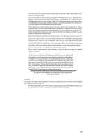
Figure 6-1 7 illustrates a generic microcontroller-based power man-
agement architecture, providing all the hardware and software functions,
as discussed above. Many trade-offs need
to
be considered when defining
this unit. Some of the regulators, like the charger, are required
to
provide
a
continuously rising level of power, which may be difficult to accommo-
date
on
board a single CMOS architecture. For example, an external P-
channel DMOS discrete transistor, such as Fairchild’s FDZ299P, housed
in
an ultra-small BGA package can help solve the problem. As illustrated in
the figure, each subsystem in the handset requires its own specific flavor
of power delivery. Low noise LDOs like Fairchild’s FAN5234 are used in
the RF section and low power LDOs like FAN2501 are used elsewhere.
This architecture also requires an efficient buck converter for the power
consuming processors as well as a boost converter in combination with
LED drivers for the LED arrays.
144
Chapter
6
Power Management
of
Ultraportable Devices
CPU
Regulator
Figure 6-18 shows the die of the FAN5307, high-efficiency DC-DC buck
converter; the big V-shaped structures on the left are the integrated P- and
N-channel MOS transistors, while the rest
of
the fine geometries are con-
trol circuitry. The FAN5307, a high efficiency low noise synchronous
PWM current mode and Pulse Skip (Power Save) mode DC-DC converter,
is designed specifically for battery-powered applications. It provides up to
300 mA of output current over a wide input range from
2.5
V
to
5.5
V. The
output voltage can be either internally fixed or externally adjustable over a
wide range of 0.7 V-5.5 V by an external voltage divider. Custom output
voltages are also available.
Figure
6-1
8
FAN5307 buck converter
Pulse skipping modulation is used at moderate and light loads.
Dynamic voltage positioning is applied, and the output voltage is shifted
0.8 percent above nominal value for increased headroom during load tran-
sients. At higher loads, the system automatically switches to current mode
PWM control, operating at
1
MHz.
A
current mode control loop with fast
transient response ensures excellent line and load regulation. In Power
Save mode, the quiescent current is reduced to
15
pA in order
to
achieve
high efficiency and
to
ensure long battery life. In shut down mode, the
supply current drops below
1
pA.
The device is stand-alone and is avail-
able in 5-lead SOT-23 and 6-lead 3
x
3 mm MLP packages.
More
on
Power Management Units
in
Cell Phones
145
Figure 6-19 shows the voltage regulator application complete with exter-
nal passive components. The integration of the power
MOS
transistors leads to
a
minimum number of external components, while the high frequency of
oper-
ations allows for
a
very small value of the passives. Appendix D provides the
data sheets of FANS307 for more technical details.
3.5
v
to
4.2
V
Li+
Figure
6-19
FANS307 application.
Low
Dropout
Block
Due to the relatively light loads (hundreds of mA rather than hundreds of
Amperes
as
in
heavy-duty computing applications), low voltages (one Li'
power source or 3.6 V typical), and often low input-to-output dropout
voltages, simple linear regulators are very popular in ultraportable applica-
tions. Figure 6-20 shows the die of the FAN2534 low dropout (1
80
mV at
150 mA) regulator:
a
state-of-the-art
CMOS
design that targets ultraport-
able applications
and is
characterized by low power consumption, high
power supply rejection, and low noise. Here again, the V-shaped structure
is the P-MOS high side pass transistor and the rest of the fine geometries
are the control logic.
In
this section, we have discussed the evolution
of
complex PMUs in
cell phones, illustrating the benefit of using the microcontroller in
sophisticated applications such
as
a
handset illumination system. We have
reviewed the breadth of mixed-signal technologies and architectures com-
ing into play, focusing on fundamental building blocks of the PMU: the
microcontroller, the buck converter, and the LDO. These, and other build-
ing blocks like LED drivers, chargers, and audio power amplifiers, can all
be integrated monolithically or in multi-chip package form to implement
a
modem handset power management unit.
From this discussion,
it
should be clear that the likely winners of the
race
for
the PMU sockets will be the companies with the broadest combi-
nation of skills and capabilities to meet the technical hurdles and the strin-
gent cost targets imposed by this market. The successful companies will
146
Chapter
6
Power Management
of
Ultraportable Devices
Figure
6-20
FAN2534
LDO
die photo.
need to have knowledge
of
ultraportable systems, power analog and digital
integration experience, and the ability to mass-produce these chips.
The Microcontroller
As discussed in the last section, the microcontroller,
a
block diagram of
which is shown in Figure 621, is the basis of
a
feature-rich, or smart phone,
power management unit. Fairchild’s ACE1 502 (Arithmetic Controller Unit)
family of microcontrollers, for instance, has
a
fully static CMOS architec-
ture. This low power, small-sized device is a dedicated programmable
monolithic IC for ultraportable applications requiring high performance. At
its core is an 8-bit microcontroller, 64 bytes of RAM, 64 bytes
of
EEPROM,
and 2k bytes of code EEPROM. The on-chip peripherals include
a
multi-
function 16-bit timer, watchdog and programmable under-voltage detection,
reset and clock. Its high level of integration allows this IC to fit in a small
SO8 package, but this block can also be up-integrated into
a
more complex
system either on
a
single die or by co-packaging.
Another important factor to consider when adding intelligence to
PMU via microcontrollers is the battery drain during both active and
standby modes. An ideal design will provide extremely low standby cur-
rents. In fact, the ACE1502 is well suited for this category of applications.
In halt mode, the ACE1502 consumes
100
nano-amps, which has negligi-
ble impact on reduction
of
battery life. Appendix E provides the data sheet
of ACE1502 for more technical details.
More on Power Management
Units
in Cell Phones
147
Figure
6-21 Microcontroller architecture.
The Microcontroller Die
The microcontroller is often the basis
of
a feature-rich, or smart phone
power management unit. Fairchild’s
ACE
1502
microcontroller die is
shown in Figure
6-22.
This
IC
fits
in
a small
SO8
package, but this block
can also be up-integrated in a more complex system, either on a single die
or
by
co-packaging.
.
Figure
6-22
ACE1502
microcontroller die.
148
Chapter
6
Power Management
of
Ultraportable Devices
Another important factor to consider when adding intelligence to
PMU via microcontrollers is the battery drain in both active and standby
modes. An ideal design will provide extremely low standby currents. In
fact, the ACE1502 is well suited for this category
of
applications. In halt
mode, the ACE1502 consumes
100
nano-amps, which has negligible
impact
on
reduction of battery life.
Processi ng Req
u
ire men
ts
As the trend continues toward convergent cell phone handsets, development
of software and firmware becomes an increasingly complex task.
In
fact,
as
the systems tend toward larger displays and the inclusion of more functions,
such as 3-D games,
a
phone’s processing power and software complexity
drive its architecture toward distributed processing. The microcontroller
adds further value in off-loading the power management tasks from the main
CPU, thus freeing it to perform more computing intensive tasks.
The application of “local intelligence,” via
a
microcontroller, can
assume various levels of sophistication, such as the recent trend of
feature
phones.
For example,
it
is common to find phones with digital cameras
built into them. However, the lack
of
a
photoflash limits the use of the
phone’s camera to brightly lit scenes. To address this problem, it is now
possible to include a flash unit built from LEDs. The addition of
a
flash
requires several functions such
as
red-eye reduction and intensity
modulation, depending
on
ambient lighting and subject distance as well as
synchronization with the CCD module for image capture. These additional
functions can be easily off-loaded to a peripheral microcontroller. Such
architecture leads to optimized power management and simplifies the
computing load
on
the main CPU.
M
i
crocon
t
rol ler- Dr iven
I I
I
u
m
i
na
t
i
on System
A complex LED based illumination system is illustrated in Figure
6-23.
Typically, an array of four white LEDs is needed for the color display back-
lighting, while another array
of
four white or blue LEDs implements the
keyboard backlighting. White LEDs, typically assembled in
a
quad pack-
age, are needed for the camera flash. And finally, an
RGB
display module
provides varying combinations of red, green,
and
blue flashes for lighting
effects. As mentioned earlier, the sequencing and duration
of
all the illumi-
nation profiles are under micro control.
Figure
6-24
demonstrates the lighting system described previously,
with all the elements of the system excited at once. The back light and
display light locations are obvious. The flash is the top light and the
RGB
is the one
in
the middle.
More
on
Power Management Units in Cell Phones
149
Figure
6-23
Handset illumination system.
Figure
6-24
Lighting system demonstration.
150
Chapter
6
Power Management
of
Ultraportable Devices
Figure
6-25
shows the typical waveform generated by the microcon-
troller to drive the lighting system. The oscilloscope waveforms are:
A
1
FLASH LED cathode signal
A2 primary back light intensity control via 8-bit PWM signal
2
3
secondary back light intensity control via 8-bit PWM signal
RGB LED Module: Red channel controlled using 4-bit PWM
signal
RGB LED Module: Green channel controlled using 4-bit
PWM signal
RGB LED Module: Blue channel controlled using 4-bit PWM
signal:
4
5
Figure
6-25
Lighting system waveforms.
6.5
Color Displays and Cameras Increase
Demand on Power Sources and Management
One
of
the most amazing recent trends in ultraportable technology is con-
vergence. With smart phones representing the convergence
of
PDAs, cell
Color Displays and Cameras Increase Demand on Power Sources and Management
151
phones, digital still cameras, music players, and global positioning systems.
With Audio Video Recorders (AVRs) converging camcorders, DSCs, audio
players, voice recorders, and movie viewers into
one
piece of equipment.
While some of these convergences will take time
to
materialize
in
the
mainstream, others are improving rapidly. One of these rapidly improving
areas is the convergence
of
two very successful ultraportable devices:
DSCs and color cell phones, into a single portable device.
This section reviews the DSC first and then dives into the integration
of this function into cell phones. Finally, the implications in terms
of
power consumption and power sources are discussed.
Digital Still Camera
Digital still cameras have enjoyed a brisk growth
in
the past few years and
today there is more of a market
for
DSCs than notebook computers. One
third of these DSCs are high resolution (higher than three megapixels);
today top
of
the
line
cameras exhibit close to five megapixels with seven
on the horizon.
Figure 6-26 illustrates the main blocks of a DSC and the power flow,
from the source (in the example one Li' cell)
to
the various blocks.
The key element in a DSC is its image sensor, traditionally
a
charge
coupled device (CCD) or more recently a
CMOS
integrated circuit that
substitutes the film
of
traditional cameras and is powered typically by a
2.8-3.3 V,
0.5
W source.
A Xenon lamp powered for the duration of the light pulse by a boost reg-
ulator converting the battery voltage up to 300 V, produces the camera flash.
The
lamp
is
initially excited with a high voltage
(4-5
kV)
pulse ionizing the
gas mixture within the lamp.
The
pulse is fired by a strobe unit composed of a
high voltage pulse transformer and firing IGBT like the SGRN204060.
The color display backlight can be powered by four white LEDs via
an active driver like the FANS613 which allows duty cycle modulation of
the LED bias current to adjust the luminosity to the ambient light, thereby
minimizing the power consumption in the backlight.
The focus and shutter motors are driven by the dual motor driver
KA7405D and the Li' battery can be charged by the FSDHS65 offline
charger adapter.
Finally powering the DSP will be accomplished by a low voltage, low
current (1.2
V,
300 mA) buck converter.
As an example, the peak power dissipated by a palm sized DSC
(1.3 megapixels) during picture taking can be around 2
W
and 1.5 W
(or
500
mA at 2.4 V) during viewing. Two rechargeable alkaline cells in series
with 700 mAh capacity can then sustain close to one hour of picture taking
and viewing.
152
Chapter
6
Power Management
of
Ultraportable Devices
Figure
6-26
Generic DSC and power distribution.
Camera Phones
If DSCs are doing well, camera phones are sizzling. It is expected that
soon the number
of
camera phones
will
surpass the number
of
DSCs
and
by 2007, one forth
of
all cell phones produced will have integrated
cameras.
The Japanese have been leading the demand
of
high-end camera
phones equipped with mega-pixel, solid-state memory cards and high-
resolution color displays.
At the time of this writing,
a
number
of
camera phones are being
announced in Japan with a resolution
of
1.3 megapixels, matching, at this
juncture, the performance of low end DSCs. Not surprisingly, forecasts for
DSCs are starting to exhibit more moderate growth rates.
Cameras for current cell phones are confined inside tiny modules and
generally meet stringent specifications, including one cubic centimeter,
100
mW power, and 2.7
V
power source and cost ten dollars.
Right now,
a
big technology battle is going
on
regarding image sen-
sors. Cell phone manufacturers are willing
to
allocate
100
mW or less
of
power dissipation to image sensors. CCDs are currently close to that limit,
while CMOS typically require half.
While at the lower resolutions, CMOS image sensors seem
to
have
won out over CCD thanks to their lower power dissipation, at the higher
resolutions (greater than one megapixel) CDD is
in
the lead.
Color Displays and Cameras Increase Demand on Power Sources and Management
153
Camera phones that are currently available have resolutions in the
0.3
megapixels range and consume pretty much the same peak power lev-
els (below
1.5
W) in call and picture mode.
Current camera phones, like DSCs, come with 8 to 16 MB memory
stick flash memory for storage. The new solid-state memory cards, dubbed
Mini SDs (Security Data), will go up to 256 MB by the end of 2005.
Based on the DSC example discussed earlier, a 1.3 megapixel camera
phone could exhibit peaks of power consumption
in
picture mode (2 W)
higher than in call mode
(1.5
W).
Such state of the art camera phones typically equipped with a 3.6
V,
1000
mAh Li' cell should warrant up to two hours of call and picture
mode.
Figure 6-27 shows the picture of
a
GSM camera phone main board
and Figure 6-28 shows the disassembled battery powering a CDMA2000
camera phone, both courtesy of Portelligent.
The trade-off for all these features is a reduction of the cell phone talk
time ability, from six hours for regular cell phones to one or two hours for
the new camera phones.
The attacks on talk time will continue as the pressure for
a
higher
number of pixels, higher resolution displays and more features incorpo-
rated into the cell phone increases.
With one
to
two hours of operation, the camera phone finds good
company
in
its bigger relative, the notebook PC: both devices badly in
need of new technologies capable
of
extending their untethered operation
time. As both rely on the same display (LCD) and battery (Li') technolo-
gies,
it
is no surprise that they also suffer from the same problem, namely
short
operation time
in
mobile mode. For the notebook to achieve its goal
of eight hours of operation and the cell phone to go back to its initial talk
time
of
six hours, we need new technologies to come to bear. Fuel cells,
electrochemical devices converting the energy of a fuel like methanol
directly
into
electricity, have the potential to store ten times the energy
of
current battery technology, and it is likely that they will be ready for prime
time
in
a couple
of
years.
On the display front, emissive technologies like Organic LEDs
(OLEDS) clearly need
to
take over from current transmissive LCD tech-
nology, thereby eliminating the power-hungry backlight outfits. The first
OLED display-based camera phone was announced
in
March of 2003.
Since
it
appears that
it
is more difficult
to
produce reliable large sized
OLED displays, this technology will probably penetrate the ultraportable
market first, before moving to the notebook and beyond.
Finally, it is worth mentioning that White LEDs are moving beyond
backlighting applications and enabling the use of flash
in
phone cameras,
154
Chapter
6
Power Management
of
Ultraportable Devices
Type
Manufacturer
Part Number
Origin
Voltage
Rating (mAh)
Weight (grams)
Pack
Size
(rnm)
Cell Count
Cell
Cost
Electronics
Packaging
Pack Cost
Figure
6-27
Camera phone mainboard example.
(Courtesy
of
Portelligent)
Li-Polymer
Sony Fukushima
UP503759
Korea
3.7
800
30.2
71.22
x
48.13
x
6.4;
1
$3.70
$0.63
$0.25
$4.58
Figure
6-28
Battery and electronics daughterboard disassembled.
(Courtesy
of
Portelligent)
Color
Displays and Cameras Increase Demand on Power Sources and Management
155
thanks
to
their greater efficiency and simplicity of operation compared to
xenon lamps.
No doubt the convergence phenomenon will continue. If high-resolution
displays, cameras, and storage cards have been the drivers
so
far,
no
less
compelling applications are on the horizon, like video on
a
handset, GPS,
and more.
Fortunately, new fechnologies are coming along that are capable of
both taming the escalation
of
power consumption (White LEDs, OLEDs)
as well as breaking the current bottlenecks (fuel cells).
Is
there an upper limit to the power consumption? Higher power con-
sumption translates directly into higher temperatures
in
the gadgets we all
love. Again, look at the notebook for an answer-in the near future we
will likely be called to bear in our hands similar temperatures to those that
we currently endure from our laptops. We expect then that our handsets
will become
as
hot
as
possible without crossing the threshold of discom-
fort,
as
cooling down is an expensive and bulky proposition.
Power Minimization
The battle for power waste-minimization extends to the signal path as
well. The logic gates, operational amplifiers, and data conversion devices
used extensively in ultraportable applications are all specifically designed
for ultra low power dissipation and are housed
in
space efficient packages.
For example, the Ultra Low Power (ULP and ULP-A) TinyLogicO
devices, such
as
Fairchild’s NC7SP74,
a
D flip-flop, and the NC7SPOO
dual NAND gate, operate at voltages between
3.3
V
and
0.9
V
and have
propagation delays as short
as
2.0
ns, consuming less than half as much
power
as
existing high performance logic.
Untethered Operation
Recent high-end handsets exhibit amazing features such
as
dual color
LCD displays, camera, video on demand, and audio on demand. An
800
mAh Li+ battery (corresponding to
a
2.4 Wh at
3
V
average output)
can sustain heavy-duty activities like playing games, taking pictures, or
recording and viewing videos-assuming each activity consumes power at
a
rate
of
1.4
W for less than two hours. Such figures of merit are getting
better, thanks to the power management methods discussed previously, but
they remain
a
far cry from the desired performance
of
6-8
hours of unteth-
ered operation
as
in
more basic handsets.
The two technologies on the horizon promising to improve this situa-
tion are organic LEDs, which do eliminate the power consuming back-
lights, and fuel cells; electrochemical devices capable of extracting
156
Chapter
6
Power Management of Ultraportable Devices
electricity directly from fuels like methanol. Fuel cells already promise to
flank Li’, for example as untethered chargers, and then to progressively
substitute Li’ technology.
Alternative power sources, such as fuel cells, will require even more
sophisticated power management. This increased management will neces-
sitate further proliferation of local intelligence to manage tasks (i.e. addi-
tional microcontrollers,; including sophisticated mixed signal capabilities
to perform supervisory functions.
Digital still cameras with OLEDs are already commercially available
and this technology is expected
to
take a wider hold in the next three to
five years. Fuel cells are a proven technology but difficult to miniaturize
and they may come
to
larger devices like notebooks before trickling down
to
handsets. Prototype handsets, some powered by, and others simply
charged by fuel cells, have been demonstrated and are expected to become
commercially viable
in
the same timeframe as OLEDs.
Power management techniques are adapting and evolving to keep up
with the increased complexities of today’s systems. These techniques
include traditional cell library regulation elements as well as untraditional
digital functions, such as bus interfaces, data converters, and
microcontrollers.
Feature-rich handsets and smart phones are clearly the devices push-
ing the edge of every technology, including power, and more features will
be coming in the future. For example, it is conceivable that a series of
“plug
and
play”
standards
will
be debated and then adopted to allow for
mix-and-match of add-on peripherals (camera,
GPS
modules, etc.) from
various sources, as well as promote the re-use of peripherals that a user
already owns. The addition of microcontrollers
in
power management
applications will become an increasingly important theme
in
the
ICs
that
provide system power for these platforms.
This “smartening” of power management electronics, combined with
the increasing maturity
of
new technologies for energy storage and dis-
plays, promises to keep these feature-rich devices
on
a steep growth curve
for
the foreseeable future.
7.1
Power Management
of
Desktop and
Notebook Computers
Power management
of
PCs is becoming an increasingly complex
endeavor. Figure 7-1 shows the progression
of
Intel PC platforms,
from the launch of the Pentium
in
1996 to current times. The Pentium
brand CPU opens up the modern era of computing however, the birth of
the CPU goes back as far as 1971 to the Intel
4004
CPU. In Figure
7-1
below each Pentium generation and associated voltage regulator
offered by Fairchild Semiconductors, we find the year
of
the platform
launch, the voltage regulation protocol (VRMxxx), the minimum fea-
ture (minimum line width drawn) of the transistors at that juncture
in
micro-meters, and the current consumption of
the
CPU.
Before Pentium, CPUs required relatively low power and could be
powered by linear regulators. With Pentium the power becomes high
enough
to
require switching regulators, devices distinctively more effi-
cient than linear regulators. With Pentium
IV
the power becomes too
high
to
be handled by a single phase (I@)-just to grasp the concept,
think of a single piston engine trying to power a car-regulator, and the
era of interleaved multiphase regulation (the paralleling and time spac-
ing
of
multiple regulators) begins. At the VRM
10
juncture, the breath-
taking pace of Moore's law has slowed down somewhat, as exemplified
by the unusual longevity of this platform. At the VRM
1
1
juncture, the
rate of increase
in
CPU power consumption has been slowed down with
sophisticated techniques such as back biasing of the die substrate, to
157
158
Chapter
7
Computing and Communications Systems
Figure
7-1
reduce leakage, new dielectric materials
to
reduce switching losses and
strained silicon,
a
technique that stretches the silicon lattice resulting in
wider passages for the electrons and hence lower ohmic resistance. In the
following session we will discuss first a Pentium
111
platform, covering
most of the basic power management technology needed for the PC. Then
we will cover
a
Pentium IV platform, focusing on new features specific to
this platform, such as interleaved multiphase and extending the discussion
to notebook systems
as
well.
Progression of CPU platforms according
to
Moore’s law.
Power Management System Solution for a Pentium
111
Desktop System
In this section we will review in detail the power management for
a
Pen-
tium I11 system, while in the next section we will focus on Pentium IV.
With PIII, the PC power management reaches a very high level of com-
plexity in terms of power management architecture. The subsequent PIV
platform doesn’t change much except for the fact that more powerful
CPUs require more hefty CPU voltage regulators.
Nine Voltage Regulators on
Board
With the
PI11
platform the motherboard needs nine distinct regulated volt-
ages, none of which are directly generated by the
ATX
silver box and all of
which consequently need to be generated locally on the motherboard. The
voltage types are as follows:
Power
Management
of
Desktop
and
Notebook
Computers
159
The Main Derived Voltages
These voltages all come from the
5
V
silver box or
3.3
V
silver box Mains
DAC controlled CPU voltage regulator
2.5
V
clock voltage regulator
1.5
V
V,
termination voltage regulator
3.3
V
or
1.5
V
Advanced Graphics Port (AGP) voltage
regulator
1.8
V
North Bridge (now renamed Micro Controller Hub or
MCH) voltage regulator
The Dual Voltages
The dual voltages are managed according to the ACPI (Asynchronous
Computer Peripheral Interface) protocol and powered from the silver box
Mains during normal operation, or from the silver box
5
V
standby during
“suspend to RAM” state.
3.3
V
Dual voltage regulator (PCI bus power)
5
V
Dual voltage regulator
(USB
power)
The Memory Voltages
Memory voltages turn
off
only during “soft off’ state.
3.3
V
SRAM voltage regulator
2.5
V
RAMBUS voltage regulator
The motherboard is becoming
too
crowded to
be
able to make room
for nine separate power supplies. The best architecture is one in which the
number of chips, and consequently the total area occupancy, are mini-
mized. Figure
7-2
shows an architecture in which four
of
the five Main
derived voltages are controlled by a single chip, while the four ACPI volt-
ages are controlled with a second chip (effectively
a
dedicated quad linear
regulator with ACPI control). The ninth regulator (North Bridge regulator)
is provided separately for maximum flexibility.
The
CPU
Regulator
The CPU regulator is by far the most challenging element
of
this power
management system. The main tricks of the trade employed to deliver high
performance with a minimum bill of materials are discussed in detail in
this section, including the handling
of
ever increasing load currents and
input voltages in conjunction with decreasing output voltages, voltage
positioning, and FET sensing techniques.
160
Chapter
7
Computing and Communications Systems
The Memory Configuration
Intel's recommended configuration for memory transition from SDRAM
to RDRAM is
2
RIMM modules and
2
SIMM modules-this points
clearly toward an architecture for the ACPI controller
in
which both
RAMBUS and SRAM voltages are available
at
the same time,
as
opposed
to an architecture in which
a
single adjustable regulator provides one or
the other.
The RCSOS8
+
RCS060 power management chipset shown
in
Figure
7-2
is
proposed as an example of
a
complete motherboard solution.
V,,,,
2
Vll7
4
A
RC5058
'
15V
15Vi3
5
A
~
-
V"15V
12V
6A
V."-
3 3
V/1
5
Y
5
VUA,h
18
A
"yl
SO24
3 3
Vll
5
V12
A
Typedet
VCI
2
5
v
2
2
5
"
2
5
"I600 m*
3
3
RCl587
I
8
vNe
2
A
5
VSTDBY
720
mA
151
3
3
V
SDRAM
Figure
7-2
Pentium
111
system power management.
Power Management System Solution
for
Pentium
IV
Systems (Desktop and Notebook)
This section reviews the main challenges and solutions for both desktop
and notebook PCs.
I
nt rod uct ion
Personal computers, both desktop and notebook, play
a
central role in the
modern communication fabric and in the future will continue that trend
toward
a
complex intertwining of wired and wireless threads (Figure
7-3)
Power Management
of
Desktop and Notebook Computers
161
Figure
7-3
PCs and notebooks
at
the center of the communication fabric.
all contributing to the ultimate goal
of
computing and connectivity any-
where anytime.
To
make the challenge even more daunting, this goal must be accom-
plished in conjunction with another imperative, “performance without
power dissipation.”
This chapter focuses on the latter challenge. Today’s state-of-the-art
technology is illustrated through the discussion of power management for
a
desktop system and
a
notebook system. We will
also
discuss future
trends toward the achievement of both goals mentioned above.
The
Power
Challenge
Moore’s law has two important consequences regarding power:
It creates
a
technology hierarchy with the CPU at the top, produced
with the smallest minimum feature (today
0.13
pm) and requiring the
lowest supply voltages
(1-1.5
V)
available thus far. Consequently, the pre-
vious CPU generation infrastructure for
0.18
pm gets recycled down the
“food chain” for memory, which is powered at voltages around
2.5
V.
The
cycle goes on and on with lower minimum features and lower voltages
continuously generated. The end result is
a
downward proliferation
of
power supply voltages from
5
V
down
to
3.3
V,
down to
2.5
V,
down to
1.5
V,
etc. This phenomenon fuels the proliferation of “distributed power.”
Every new generation motherboard has more functions and requires more
voltage regulators than the previous one, while at the same time the moth-
erboard form factor is shrinking to meet the new demands for slick form
factors.
162
Chapter
7
Computing and Communications Systems
By stuffing more and more transistors
in
a die (a Pentium
IV
CPU
in
2004 has 42 million transistors versus 2300 transistors in 197
1
for the Intel
4004 CPU) modern devices create tremendous problems
of
heat and
power dissipation which must be resolved by us, the power specialists.
This phenomenon has generated a tremendous migration from inefficient
power architectures like linear regulators (believe
it
or
not, the first CPUs
were powered by Low Drop Output regulators,
or
LDOs, notorious for
their high losses) to more efficient ones like switching regulator architec-
tures. The workhorse for switching regulators continues to be the buck,
or
step down converter, continuously renewing itself into more powerful
implementations, from conventional buck to synchronous to multiphase,
in order to keep up with the CPU growing power.
Both trends compound the same effect, a phenomenal concentration
of heat on the chips and on the entire motherboard that cannot continue
untamed. More
on
this subject will be discussed later.
Desktop Systems
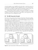
Figure 74 and Figure 7-5 illustrate a modern desktop system in its main
components: the microprocessor, the Memory Channel Hub (MCH, also
referred to as North Bridge), and the
YO
Hub (IOH
or
South Bridge), con-
necting
to
the external peripherals. While the silver box can only provide the
“row” power
(5
V,
3.3
V,
and 12
V),
most of the elements in the block dia-
gram need specialized power sources, to be provided individually and
locally. Going from wall to board, an impressive slew
of
processes and tech-
nologies come to bear, from high voltage discrete DMOS transistors
to
Bipolar and Bi-CMOS IC controllers, from power amplifiers to linear and
switching regulators. They all fall under a centrally orchestrated control pro-
viding energy
in
the most cost effective and power efficient way possible.
Powering the CPU
By far the most challenging load on the motherboard is the CPU. The
main challenges in powering a CPU are:
Duty
Cycle
High input voltages
(12
V)
and low output voltages (1.2
V
typically) for
the regulator, leading to duty-cycles
of
10
percent
(Vou+VrN
=
0.1). This
means that useful transfer of power from the 12
V
source to the regulated
output happens only during
10
percent of the time period. For the
remaining
90
percent
of
the time the load is powered only by the output
bulk capacitors (tens
of
thousands
of
microFarads).
Power Management
of
Desktop
and
Notebook Computers
163
Figure
7-4
Desktop
PC
motherboard.
Figure
7-5
Desktop system.
So
far, the introduction of interleaved multiphase buck converters has
helped reduce the number of both input and output bulk capacitors. Still, the
amount of capacitors used today is huge and the current trend
is
racing
toward faster architectures and technologies capable
of
reducing the size of
164
Chapter 7 Computing and Communications Systems
the passive elements without compromising the efficiency of the regulator,
which must remain near
80
percent. This efficiency requirement also puts
the discrete technology on the front line: it will take
a
new generation
of
dis-
crete DMOS transistors with sensibly lower switching losses to achieve this
goal. The desirable endpoint is elimination
of
electrolytic capacitors-the
current workhorse
of
bulk capacitors-in favor of an all-ceramic solution.
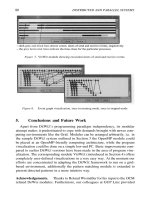
Tight Regulation
Output voltage is tightly regulated. The voltage across the CPU is allowed
to vary over production spreads and under wide and steep load transients
(30
A/p)
for only
a
few tens of millivolts.
One industry standard practice, in order to alleviate the problem of eat-
ing up the voltage margins due to voltage spikes during load transients, is
the utilization of
a
controlled amount of output “droop” under load. The
waveform in Figure
74(a)
shows the normal behavior of
a
regulated output
in absence of droop, exhibiting
a
total deviation of
2
x
ESR
x
I,
where
I
is
the current and
ESR
is the series resistance of the bulk capacitor
C.
By add-
ing
a
droop resistor
RDROOp
in the indicated position and of value equal to
ESR (RDROOp
=
ESR)
the total deviation is reduced
to
ESR
x
I
as
the (b)
waveform illustrates. It follows that the waveform (b) will have
a
total devi-
ation equal to the waveform
(a)
at twice the
ESR
value, corresponding to
half the amount
of
output bulk capacitors. The technique has been illustrated
here with passive droop via
RDROOp
Since passive droop is dissipative, the
best practice is
to
do “active droop” or drooping
of
the output
by
controlled
manipulation
of
the VRM load regulation, yielding the desired reduction in
BOM at no efficiency cost. Finally,
as
the output voltage droops under load,
less voltage and proportionally less power is delivered to the load, leading to
a
sensible reduction in total system power dissipation.
Dynamic Voltage Adjustment
Dynamic voltage adjustment
of
the output is done via
D-A
converter on
the order
of
hundreds of nanoseconds to accommodate transitions to and
from low power modes.
Our architecture, valley control, exhibits
a
very fast transient response
and hence fits this type of application very well.
Figure
7-7
illustrates valley current-mode control based on leading-
edge modulation. The error amplifier forces
Vour
to equal
VREF
at its
input. However, contrary to the standard peak control technique, now its
output voltage, V,, is compared
to
the low-side MOSFETs current
(IL)
times RDSON. When
I,
x
RDsoN falls below the error voltage, the PWM
comparator goes high. This sets the flip-flop, initiating the charge phase by
turning on the high-side driver and terminating the discharge phase by
turning off the low-side driver. The charge phase continues until the next
Power Management
of
Desktop and Notebook Computers
165
Vo
=
Vo
-
ESR'1
7
@
RORWP=ESR
I
I
Figure
7-6
Output voltage "droop" reduces BOM by fifty percent.
SQ
COMPO
-
v
R
Q#
-
CK
'I
RIJSON
-
-+
-
-
ROSON'IL
AV
=
1
Valley
Control
I
Figure
7-7
Valley control architecture.
clock pulse resets the flip-flop, initiating
a
new discharge phase. The
advantage
of
this architecture is that
it
easily senses the current on the
low side driver, where the current is present for
90
percent
of
the time in
a
10
percent duty cycle application like this.
For
example
if
the clock
frequency is
300
kHz, the high side pulse is only
330
ns,
whereas the
low
side pulse is
2.97
p.
Consider
also
that sensing
a
330
ns
pulse
on
the
low side driver would correspond to operate the VRM at
a
frequency
of
2.7
MHz,
a
measure
of
how fast valley control can operate compared to
peak control.
166
Chapter
7
Computing
and
Communications Systems
The turn-on
of
the high side driver is instantaneous and asynchronous
as opposed to peak control
in
which the turn-on can
only
happen at every
clock edge. It follows that standard peak control has inherently a delay
of
one clock period (say
3.3
ps
at
300
kHz), whereas valley control has fast
response
(200
ns) independently of the clock.
This architecture is proposed both
in
Fairchild’s line
of
fully
inte-
grated converters, having controllers and drivers
on
board (Figure
7-8),
as
well as in the new line of controllers and separated drivers (Figure
7-9).
Current Sensing
In modern voltage regulator modules precision current sensing is critical
for
two reasons: without precision current sensing there is
no
accurate
“active droop” and there is
no
good current sharing
in
interleaved mul-
tiphase controllers.
The easiest way
to
accomplish precise current sensing would be to
utilize a precise current sense resistor but because of cost and power dissi-
pation issues, this isn’t a practical solution.
Mainstream solutions today accomplish current sensing
in
a
“loss-
less” fashion by measuring current across the drain-source
ON
resistance
of
the discrete DMOS transistor (Figure
7-7).
This method eventually will
run out
of
steam because of the temperature dependency
of
this resistance
(more than sixty percent over 100°C roughly.) Other methods like the one
measuring current on the basis of the inductor parasitic resistance are no
better over temperature.
A few brute force techniques are starting to appear
in
response
to
this
problem, including the use of external thermistors, diode temperature sen-
sors,
etc. There is
a
simple way to accomplish precise current sensing,
namely the ratioed Sense-FET technique. This technique exploits the cel-
lular nature of
a
modern DMOS discrete transistor
in
order
to
isolate
a
small portion of
it
into
a separate source capable
of
reflecting current
in
a
predictable amount with respect
to
the main transistor. This technique has
not taken over
in
VRMs yet because
until
now
it
was not needed and
because an earlier attempt
at
an industry standardization
of
this device
failed. Probably the time has come to revisit this technology.
Powering the Entire Motherboard ACPI
Advanced Configuration and Power Interface (ACPI) is an open industry
specification co-developed by Compaq, Intel, Microsoft, Phoenix, and
Toshiba. ACPI establishes industry-standard interfaces for OS-directed
configuration and power management on laptops, desktops, and servers.
The specification enables new power management technology to
evolve
Power
Management
of
Desktop
and
Notebook
Computers
167
Figure
7-8
FAN5093/FAN5 193
two-phase monolithic controller and
driver.
Figure
7-9
FAN5019
+
FAN5009
up
to
four-phase controller and
separate drivers.