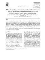
Studies of self assembled monolayers on highly oriented pyrolytic graphite using scanning tunneling microscopy and computational simulation 3
Bạn đang xem bản rút gọn của tài liệu. Xem và tải ngay bản đầy đủ của tài liệu tại đây (279.09 KB, 14 trang )
CALIBRATION
CHAPTER 3
CALIBRATION OF SCANNING TUNNELING MICROSCOPY USING
HIGHLY ORIENTED PYROLYTIC GRAPHITE AS STANDARD
3.1 Purpose of Calibration
The scanning tunneling microscope (STM) is the ideal instrument for surface
investigations of matter on an atomic scale. The most quantitative information
obtained by STM is the geometry and physics of surface topography, including the
roughness of microstructures [1, 2]. Incorrect lateral calibration of the STM scanning
elements will cause the images to be stretched, compressed or even skewed. Thus it is
crucial to have accurate calibration to achieve reliable STM images.
Several factors can cause the distortion of the STM images, including
temperature and humidity which affect the piezoceramic’s sensitivity, hysteresis of the
system, thermal drift, the sharpness of the STM tip, and noise. In order to minimize
these effects, a very sharp Pt/Ir tip was used throughout scanning process. The
vibration isolation system is in operation during the experiment to isolate the vibration
from the environment. The experimental room is equipped with air-conditioners and
dehumidifier to control the temperature and humidity respectively.
Some works have been carried out regarding the calibration of STM. Jorgensen
and coworkers [3] developed a technique based on detection of the reciprocal unit cell
in Fourier space for estimating the lateral calibration factors and the drift in the fast
scanning direction. Desogus and coworkers used a capacitive sensor coupled to a
38
CALIBRATION
STM piezoscanner for accurate measurements [4]. Lapshin also described a practical
method to find automatically the calibration coefficients and residual
nonorthogonality of STM [5]. Wang et al employed the combination of STM and
X-Ray interferometer for calibration [2]. There are also some computational methods
developed for data analysis to remove the distortion [6, 7]. However, these methods
are not suitable for our experiments, either due to their complexity or incompatibility
with our instruments. Here we present a simple calibration procedure by improving
the original calibration method developed by Veeco Instruments.
3.2 Piezoelectricity and Scanner
Piezoelectricity is the ability of some materials (deleted) to generate an electric
potential in response to applied mechanical stress. This may take the form of a
separation of electric charges across the crystal lattice. The piezoelectric effect is
reversible, exhibiting the direct piezoelectric effect (the production of electricity when
stress is applied) as well as the converse piezoelectric effect (the production of stress
and/or strain when an electric field is applied). Lead zirconate titanate (PZT) crystal is
a ceramic perovskite material that shows a marked piezoelectric effect [8].
The effect finds useful applications such as the production and detection of sound,
generation of high voltages, electronic frequency generation, microbalance, and ultra
fine focusing of optical assemblies. It is also the basis of operation of the scanning
probe microscope, such as STM and AFM.
Scanner serve as the “movers and shakers” of every scanning probe microscope.
39
CALIBRATION
Typically, they consist of a hollow tube made of piezoelectric material such as PZT
[9]. Piezo materials contract or elongate when a negative or positive voltage is applied
depending upon the orientation of the material’s polarized grain structure. The
scanners are used to manipulate the sample-tip movement very precisely to scan the
sample surface. In some models (e.g., Small Sample MultiMode) the scanner tube
moves the sample, with the tip set stationary. In other models (e.g., Dimension SPMs)
the sample is stationary and the tip is moved.
The different scanners do not react exactly the same to a voltage. Because of
slight variations in the orientation and size of the piezoelectric granular structure
(polarity), material thickness, etc., each scanner has a unique property [9]. This
property is conveniently measured in terms of sensitivity, a ratio of piezo
voltage-to-piezo movement. Sensitivity is not a linear relationship, because piezo
scanners exhibit a larger sensitivity (i.e., more movement per volt) at higher voltages
than they do at lower voltages. This non-linear relationship is determined for each
scanner crystal. As the scanner ages, its sensitivity will decrease and periodic
recalibration becomes necessary.
The response curve of piezo-materials to applied voltage curve is presented in Fig
3.1. This curve typifies scanner sensitivity across the full range of movement. The
vertical axis denotes the voltage applied to the scanner [9] while the horizontal axis
denotes the scanner movement. At higher voltages, the scanner’s sensitivity increases
(i.e. more movement per voltage applied), whereas the scanner is “motionless” at zero
volts. Plotting each point along the curve describes a second-order, exponential
40
CALIBRATION
relationship which provides a rough approximation of the scanner sensitivity.
Fig 3.1 Diagram showing the response curve of piezo-materials to applied voltage curve [9]. The
vertical axis denotes the voltage applied to the scanner while the horizontal axis denotes the
scanner movement. The scanner’s sensitivity is not linear, with larger sensitivity at higher voltage.
3.3 Calibration of STM
3.3.1 Calibration Methods
For purposes of calibration, the manufacturer employs various derating and
coupling parameters to model the scanners’ nonlinear characteristics. By precisely
determining the points along the scanner’s sensitivity curve, and through the
application of a rigorous mathematical model, the full-range measuring accuracy can
be made (deleted) better than 1 percent.
Because the scanner sensitivities vary according to the voltage applied to them,
the reference must be thoroughly scanned at a variety of sizes and angles. The user
then specifies the distance between known features on the reference’s surface and a
parameter is recorded to compensate the scanner’s movements The X, Y and Z axes
may be calibrated in any sequential order.
41
CALIBRATION
The calibration procedure consists of three steps. Firstly, a calibration reference
having surface features of precisely known dimensions is scanned. These dimensions
are compared with those estimated by the SPM software; and the calibration
parameters are adjusted until the SPM’s dimensions meet the true dimensions of the
reference.
The “A” scanner is the smallest scanner, with a total travel distance of
approximately 0.4m along each axis. Its compact design provides excellent stability
for atomic scans. Based on the previous method developed by the manufacturer, we
developed a relatively simple methodology to perform calibration of the “A” scanner
for scanning tunneling microscope function.
3.3.2 Calibration Procedures
The calibration of STM can be conducted with a standard sample: highly ordered
pyrolytic graphite (HOPG). The HOPG needs to be cleaved prior to the scanning.
Cleaving was accomplished by the adhering of a tape to the surface and then having it
peeled off, which produced a fresh surface of atoms having a regular lattice. The
sample to be used was placed on a puck and then attached to the scanner cap.
The surface was engaged by the tip. The Intergral Gain and Setpoint are adjusted
to obtain good images. The scanner was allowed to stabilize by scanning 2-3 frames.
If the scanner has been running at extreme voltages, the stabilization time might take
longer. The Setpoint is kept low if possible. In our calibration, its value is set between
30-50pA. The Z Center Position is set to 0V. The scan rate is set quite high (~12Hz)
42
CALIBRATION
for atomic scale images to reduce some of the noise due to thermal drift.
The condition of the tip is critical for obtaining a good STM image with atomic
resolution. Fig 3.2 is a typical STM image of HOPG scanned with a poorly prepared
Pt-Ir tip.
Fig 3.2 STM image of a cleaved HOPG scanned with a poorly prepared Pt-Ir tip prior to
calibration (6×6 nm, V
bias
=80mV, I
offset
=30pA)
If difficulty is experienced obtaining an image, a different Pt-Ir tip will be
installed until the image of carbon atoms can be roughly observed. Fig 3.3 shows a
STM image of HOPG scanned with a good Pt-Ir tip.
43
CALIBRATION
Fig 3.3 Typical STM image a clean HOPG scanned with a good Pt-Ir tip prior to calibration (6×6
nm, V
bias
=80mV, I
offset
=30pA). Image was treated with Lowpass function of the Nanoscope IIIa
software to remove noise.
The alignment of the graphite crystal on the working platform was not always
ideal; it resulted in the angle between the measured direction and horizontal direction.
Therefore the line containing the highest number of bright carbon atoms was selected
for distance measurement. The section analysis (Fig 3.4) of the distance profile along
the white arrow in Fig 3.3 showed that the average distance between neighbouring
bright carbon atoms was 0.267nm.
44
CALIBRATION
Fig 3.4 Section Analysis of the STM image in Fig 3.3 along the orientation of the white arrow
Fig 3.5 shows the standard parameters of the graphite surface lattice, where the
real atomic spacing between neighbouring bright carbon atoms is 0.246nm. The
difference between the measured distance and the literature value was 8.5%, which
was more than the allowed error of 2.0%. Thus, the calibration procedure had to be
carried out to ensure the measuring error of the STM measurements fall within the
allowed value.
Fig 3.5 Schematic diagram of atomic spacing on the HOPG surface under STM. Each circle
represents one bright carbon atoms.
45
CALIBRATION
The calibration parameters were listed in Fig 3.6. Among them the ‘X fast sens’,
‘Y fast sens’, ‘X slow sens’ and ‘Y slow sens’ should be modified accordingly. We
started with “X fast sens” when the scan angle was set at 0°.
The new “X fast sens” value
=
valuesensfast valueoriginal
distance measure
d
distance ltheoretica
=
814.2100.3
271.0
246.0
The new values of “Y slow sens” (at 0°, vertical direction), “Y fast sens” (at 90°,
horizontal direction) and “X slow sens” (at 90°, vertical direction) were also
calculated. After four new parameters were employed, the STM images of HOPG
were captured again after scanning for a certain period of time when whole work
station became stable.
Fig 3.6 Calibration parameters of scanner A
The new value of spacing between the adjacent bright carbons was recalculated.
46
CALIBRATION
If the difference between the experimental result and the literature value was still
larger than 2%, a re-calibration was necessary. Fig 3.7 shows the final graphite image
obtained by the STM after repeating several times of calibration procedures. The
measured distance between adjacent bright carbon atoms was 0.250nm, as shown by
the section analysis, which was within the allowed range of 0.241 to 0.251nm. The
calibration was considered successful and subsequent experiment would be carried
out using the same set of parameters obtained based on the latest calibration.
Fig 3.7 STM image of HOPG after calibration with a good Pt-Ir tip (6×6nm, V
bias
=80mV,
I
offset
=30pA). Image was treated with Lowpass function of the Nanoscope IIIa software to remove
noise.
47
CALIBRATION
Fig 3.8 Section Analysis of the STM image in Fig 3.7
3.4 Discussion
The calibration of the STM is particularly important in our experiment and a
chapter is therefore dedicated to this subject. The calibration method provided by the
manufacturer has been modified. For example, for the parameter of “X fast sens”, we
are supposed to measure the distance horizontally. However, in most calibration
procedures it is difficult to position the graphite crystal at the correct angle to carry
out the measurements. Instead, the distance along the line of highest atom density
white arrow shown in Fig 3.3 was measured. The calibration can be easily done by
repeating that method several times, without spending time on positioning the
graphite crystal on the scanner platform.
During the scanning process, the tip moved in two directions: from the top of the
image to the bottom of the image, and in the opposite direction. It was observed that
48
CALIBRATION
the images obtained when the tip moves in the opposite directions were different. This
could be due to the asymmetric form of the STM tip. The Pt/Ir tip was usually cut
mechanically along the 45° angle, and therefore the tip did not have a symmetric
shape. In addition the STM tip was not perpendicular to the scanning surface in most
cases, as shown in Fig 3.9.
Fig 3.9 Illustration of contact between the STM tip and the HOPG surface
As the STM images were scanning-direction dependent, only images at one
scanning direction were collected to ensure the consistency of the experimental results.
The STM images can also be affected by the height of the sample. When the height of
the sample was changed, the STM head had to be adjusted, which in turn changed the
orientation of Pt/Ir tip and caused distortion of the images. It is important to keep the
sample height constant during the whole experiments. Hence, the same HOPG crystal
was used throughout the experiment, including calibration, SAMs preparation and
STM measurements.
Furthermore, the piezoceramic component is very sensitive to the environment,
49
CALIBRATION
such as temperature and humidity. The working environment has been equipped with
air conditioner and dehumidifier to provide the constant temperature and humidity for
STM instruments. It was also strongly recommend that all the data should be collected
on the same day for one sample.
3.5 Conclusion
In short, by modifying the original calibration methods provided by the
manufacturer, we developed the calibration procedures which are more convenient for
users. Due to the complexity and sensitivity of the STM components, calibration must
be carried out every time before studying of the surfaces to ensure the reliability of
the experimental results.
50
CALIBRATION
51
References
[1] Pope, K.J.; Smith, J.L.; Shapter, J.G. Smart Mater. Struct. 2002, 11, 679.
[2] Lin, W.; Kuetgens, U.; Becker, P.; Koenders, L.; Li, D.C.; Cao, M.
Nanotechnology 1999, 10, 412.
[3] Jorgensen, J.F.; Madsen, L.L.; Garnaes, J.; Carneiro, K.; Schaumburg, K.
J. Vac.
Sci. Technol. B 1994, 12, 1698.
[4] Desogus, S.; Lanyi, S.; Nerino, R.; Picotto, G.B.
J. Vac. Sci. Technol. B 1994, 12,
1665.
[5] Lapshin, R.V.
Rev. Sci. Instrum., 1998, 69, 3268.
[6] Andersen, J. E. T.; M
øller, P. Surf. Coat. Technol. 1994, 67, 213.
[7] Lapshin, R.V.
Meas. Sci. Technol. 2007, 18, 907.
[8] Gandhi, M.V.; Thompson, B.S.
Smart Materials and Structures, London:
Chapman & Hall,
1992, 1
st
edition.
[9] Digital Instruments, Support Note No. 217, Rev. D