- Trang chủ >>
- Khoa Học Tự Nhiên >>
- Vật lý
Morphology and growth mechanism study of self assembled silicon nanowires synthesized by thermal evaporation
Bạn đang xem bản rút gọn của tài liệu. Xem và tải ngay bản đầy đủ của tài liệu tại đây (538.13 KB, 7 trang )
Morphology and growth mechanism study of self-assembled
silicon nanowires synthesized by thermal evaporation
Z. Zhang
1
, X.H. Fan, L. Xu, C.S. Lee, S.T. Lee
*
Center of Super-Diamond and Advanced Films & Department of Physics and Materials Science, City University of Hong Kong,
83 Tat Chee Avenue, Kowloon, Hong Kong, People's Republic of China
Received 18 December 2000; in ®nal form 8 January 2001
Abstract
Silicon nanowires (SiNWs) grown from `sun¯ower-seed'- and `mushroom'-shaped particles have been observed by
electron microscopies. The SiNWs were synthesized by thermal evaporation of SiO powders without any metal cata-
lysts. The SiNWs grown on the sun¯ower-seed-shaped particles had sub-branches of SiNWs terminated by Si bulbs.
The SiNWs on the mushroom-shaped particles were densely and uniformly distributed on the surface of the mushroom
cone. The growth history suggests that these SiNWs were formed by nucleation which originated from the surface of
amorphous SiO particle matrixes via phase separation and precipitation followed by growth through oxide-assisted
vapor±soild reaction. Ó 2001 Elsevier Science B.V. All rights reserved.
1. Introduction
The electronic, magnetic, optical and chemical
properties of nano-materials can be very dierent
from their bulk counterparts and depend sensi-
tively on their size, shape and composition. For
example, bulk silicon is very good in electronic but
poor in light emission properties at room temper-
ature, because of its indirect band gap of $1.1 eV
and a small exciton binding energy ($15 eV). In
contrast, silicon nanowires (SiNWs) of a few na-
nometers in diameter have shown unusual photo-
luminescence and Raman spectra [1±4], implying a
strong quantum size con®nement eect which re-
laxes the k-selection rule to overcome the indirect
nature of optical transition. In addition, lithium
doping of SiNWs [5] has a promising application
in energy storage as advanced battery cell materi-
als.
The size, shape and structure of SiNWs depend
sensitively on their composition, as well as the
temperature and other parameters of the synthetic
process. The experimental results of thermal
evaporation synthesis have shown that SiNWs are
rich in morphology in dierent deposition tem-
perature regions under the same process condition.
The variation of morphology not only exists in the
diameter distribution from 10±100 nm, but also in
the diversity of shapes from octopus-like, chain-
like, spring-like, tadpole-like, to single wires with a
constant diameter [6±9]. Though the formation
and structure characterization of those SiNWs
of dierent morphologies have been extensively
30 March 2001
Chemical Physics Letters 337 (2001) 18±24
www.elsevier.nl/locate/cplett
*
Corresponding author. Fax: +852-2784-4696.
E-mail address: (S.T. Lee).
1
On leave from Beijing Laboratory of Electron Microscopy,
Center of Condensed Matter Physics, Institute of Physics,
Chinese Academy of Sciences, P.O. Box 2724,100080, Beijing,
China.
0009-2614/01/$ - see front matter Ó 2001 Elsevier Science B.V. All rights reserved.
PII: S 0 0 0 9 - 2614(01)00183-X
investigated recently by transmission electron mi-
croscopy (TEM), the growth mechanism related to
various morphologies remains an open question.
One of the reasons is that since SiNW specimens
for TEM examination are normally chosen and
removed from speci®c regions of a substrate where
they have been deposited, the growth history re-
lated to the as-deposited position cannot be traced
to the whole deposition-collecting-substrate re-
gions under dierent temperatures. Accordingly,
we apply scanning electron microscopy (SEM) to
investigate the morphology variation of SiNWs
directly at their original deposited sites and carried
out chemical analysis by X-ray energy dispersion
spectroscopy (XEDS). Although SEM cannot
provide the high spatial resolution images of the
SiNW structure achievable by TEM, it neverthe-
less can allow a systematic study of the growth
process in dierent temperature zones directly at
the original deposition locations.
Thus far, oven-laser ablation [10±13] and ther-
mal evaporation [14±17] are two methods nor-
mally used for the synthesis of SiNWs. The key
point in these two methods is the formation of a
sucient amount of silicon atoms and/or silicon
oxide clusters in gas phase from the target powders
of silicon or silicon oxide by laser ablation or high
temperature evaporation. A growth mechanism
for these two cases is the vapor±liquid±solid (VLS)
model, in which a metal catalyst (Ni or Fe) liquid
droplet plays the central role in dissolving/ab-
sorbing the vapor-phase silicon atoms and/or sili-
con oxide clusters. When the Ni(Fe)Si
2
droplet
reaches supersaturation after dissolving sucient
silicon atoms from the gas phase, precipitation of
silicon nanowires from the droplet can be induced.
Based on a systematic analysis of the growth
mechanism of semi-conductor nanowires, Lee et al.
[18] proposed an oxide-assisted model by which
the SiNWs were formed in two steps. Firstly,
amorphous nanoparticles of SiO are nucleated on
the surface of SiO matrix particles, followed by
phase separation and successive silicon precipita-
tion due to the disproportionation or oxidation±
reduction reaction of amorphous SiO in the tem-
perature range 950±1250°C. Secondly, the amor-
phous nanoparticles of SiO at the tips of SiNWs
continuously absorb Si±O clusters from the gas
phase, which ensures the continual phase separa-
tion and precipitation and results in the formation
of SiNWs made of a Si core and a SiO
2
sheath.
The one-dimensional growth of SiNWs is facili-
tated by the SiO
2
sheath that con®nes the lateral
growth of SiNWs, and the high absorptivity for
Si±O clusters of the molten SiO nanoparticle at the
tip as a growth front [18]. The semi-liquid nature
of the SiO tip is due to melting point lowering
induced by the nanosize eect associated with the
SiO nanoparticle. Actually, phase separation and/
or precipitation of both silicon and SiO
2
crystal-
lites in nanometer size have been well documented
in the literature [19±21].
In the present Letter we report a systematic
SEM study of SiNW growth history related to the
morphology and growth temperature. We show
that the formation of SiNWs is indeed closely re-
lated to the amorphous SiO particles, and the
growth and self-assembling process of SiNWs on
the surface of SiO particles strongly support the
oxide-assisted growth model of SiNWs with vari-
ous morphologies [18].
2. Experimental
To study the growth history and related mech-
anism, silicon substrate wafers used as SiNWs
collectors were arranged in the temperature re-
gions ranging 600±1350°C within the furnace. The
relationship of SiNW morphology to dierent
temperature zones on the substrate was analyzed
with SEM (Philips SEM FEG Model XL30). The
possible impact of chemical composition on the
morphology of SiNWs was investigated by using
X-ray energy dispersion spectroscopy (XEDS) at-
tached to the SEM. The thermal evaporation
condition for SiNWs synthesis was the same as
that reported previously [8] but with a growth time
of 10 min. The short synthesis time was used so as
to study the initial stage of SiNW growth.
3. Results and discussions
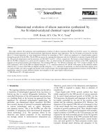
Fig. 1 shows the SEM images of SiNWs and
particles on the Si substrate at a temperature of
Z. Zhang et al. / Chemical Physics Letters 337 (2001) 18±24 19
around 1000°C. The composition of the particles
was con®rmed by XEDS to be Si
m
O
n
with a m/n
ratio close to 1:1. Careful microstructure exam-
ination shows that the Si substrate serves only as
a collector for SiNW deposition having no other
relationship to SiNWs. A characteristic feature of
Fig. 1 is that the SiNWs are grown either radially
outward from the particle (Fig. 1a) or in some
preferred directions (Fig. 1b). The SEM images
reveal a close relationship between the SiNWs
and SiO particles in that all visible SiO particles
are always connected to SiNWs, as evident from
Fig. 1b. Another noticeable feature is that many
more SiNWs appear on the surface of larger
particles, as is clear from Fig. 1a at higher mag-
ni®cation.
The relationship between the SiNWs and SiO
particles can be seen more clearly from Fig. 2a,
which shows that SiNWs are grown directly from
the surface of a SiO particle. In addition, each
SiNW has a nanoparticle at its tip while its root is
connected to a hole on the particle surface. Fig. 2b
is an SEM image from the same region in Fig. 1a
but with a high magni®cation, which shows clearly
the initial growth stage of SiNWs from the surface
Fig. 2. (a) and (b) An initial growth stage of SiNWs can be
found from fresh SiO particles and (c) `C' indicates a piece
unfolded from the left side of the ®gure.
Fig. 1. SEM images of SiNWs deposited on Si at about 1000°C.
(a) SiNWs are connected and grown radially outward from the
surface of the particle: and (b) some SiNWs show preferred
growth directions from dierent sized particles.
20 Z. Zhang et al. / Chemical Physics Letters 337 (2001) 18±24
of SiO particles. The initial growth stage of SiNWs
can be further visualized from Fig. 2c. The clean
surface (marked by letter C) was produced by
unfolding from a grown surface layer as shown in
Fig. 2a,b, thus it remains relatively clean as it re-
ceived little exposure to the growth ambient. On
the other hand, the covered layer is full of SiNWs,
while the curved edge of the unfolded layer (de-
noted by an arrowhead in Fig. 2c) is also relatively
free of SiNWs.
In accordance with previous TEM studies
[12,18,22], the above SEM results provide further
experimental evidence that the nucleation sites of
SiNWs are on the surface of a SiO matrix, where
the amorphous SiO nanoparticles are formed, and
successive phase separation (or disproportiona-
tion) and precipitation occur under suitable tem-
perature and chemical composition.
Due to the morphological sensitivity of SiNWs
to the growth temperature and composition, many
types of SiNWs can be formed, rendering the de-
termination of the growth mechanism of SiNWs
more dicult. Fig. 3a is a low-magni®cation SEM
image of SiNWs deposited on the Si substrate at a
temperature about 1200°C. A characteristic fea-
ture of this image is that there are some sun¯ower-
seed-shaped particles, with the size of about
0:2 Â 0:5mm
2
. In the vicinity of this type of par-
ticle, there are also some small particles with ir-
regular shapes. These particles are connected by
many relatively straight SiNWs of uniform diam-
eter as strands, as shown in Fig 3b. Images at
higher magni®cation in Fig. 3c show that the
surface of the particles is fully covered with self-
assembled SiNWs. A careful examination of the
image at still higher magni®cation (Fig. 3d) shows
Fig. 3. (a) Self-assembled SiNWs are grown on the surface of sun¯ower-seed-shaped SiO particles; (b) straight SiNWs are found
connecting these particles; (c) SiNWs have characteristic sub-branches of SiNWs; and (d) silicon bulbs are found at the tips of the
SiNWs sub-branches.
Z. Zhang et al. / Chemical Physics Letters 337 (2001) 18±24 21
the self-assembled SiNWs to have many sub-
branches of SiNWs grown out from their surface.
The sub-branches of SiNWs are all terminated by
Si bulbs, making them dierent from those SiNWs
reported before [5,6]. The average diameter of the
main branch of SiNWs is in the range 40±60 nm,
and that of the sub-branch of SiNWs is 30±40 nm.
The bulb on the tip of the sub-branch is less than
100 nm in diameter. The sub-branch SiNW is thin
and normally curved at the region close to its
connecting point with the main branch of SiNWs,
and its diameter increases gradually to form the
bulb at its tip. HREM results reveal that the main-
and sub-branches of SiNWs are clothed with a
SiO
2
out-layer of a few nm in thickness. HREM
and electron diraction results show that the bulbs
also have a silicon core and an amorphous SiO
2
outer layer. A systematic XEDS analysis shows
that the sun¯ower-seed-shaped particles are com-
posed of silicon and oxide only, while the oxygen
content varies from the top to bottom of the par-
ticles. The oxygen content decreases from 54 at.%
at the head of the seed particle (denoted by letter
H), to 45 at.% at the middle (noted as M), and
down to 34 at.% around the bottom of the parti-
cles (marked as B). The oxygen content of the
particles implies that the SiNWs were nucleated
and grown from the sun¯ower-seed-shaped SiO
x
particles. This again supports the oxide-assisted
growth model of SiNWs.
The dependence of SiNW morphology on
temperature can also be extracted from the fea-
tures revealed in the temperature region of
1180°C, where particles with the mushroom shape
are observed on top of silicon substrates, as
shown in Fig. 4a. SEM image at higher magni®-
Fig. 4. (a) SiNWs covered mushroom-shaped SiO particles deposited at 1180°C, (b) a mushroom-shaped particle, (c) SiNWs on the
smooth cone surface of a mushroom-shaped particle, and (d) many straight and parallel SiNWs connecting a mushroom-shaped
particle and another particle nearby (possibly a piece broken o from the former).
22 Z. Zhang et al. / Chemical Physics Letters 337 (2001) 18±24
cation (Fig. 4b) shows that these particles have a
cone shape pussy surface and the top surface of
the cone is rather rough. Fig. 4c is the SEM im-
age of the mushroom-shaped particles at still
higher magni®cation, which shows clearly that the
surface is full of self-assembled SiNWs 30±40 nm
in diameter. SiNWs at the top surface of the
mushroom particles are smaller in diameter. Al-
though HREM studies con®rm these curved
nanowires to be SiNWs, XEDS analysis reveals
an obvious change in oxygen content from 54
at.% at the bottom to 27 at.% at the top surface
of the mushroom particles. That is the Si/O ratio
changes from about 1:1 to 3:1. There are two
possibilities for the higher oxygen signals by
XEDS at the bottom (denoted by letter B) and
middle (marked as H) than that at the top (T)
parts shown in Fig. 4b. Firstly, though the outer
shell of SiNWs on the cone surface at regions B
and H has the same chemical content as that in
the region T, the inner part underneath the outer
shell of the former has a higher oxygen content,
thus giving rise to an XEDS signal rich in oxygen.
A second possibility is that the SiNWs on the
surface of the mushroom particles indeed have a
dierent oxygen content.
Fig. 4d shows that a mushroom-shaped particle
and a piece nearby (apparently separated from the
former) are connected by many straight SiNWs.
The string-like SiNWs connecting the two particles
may be understood as follows. While the SiNWs
grown directly and self-assembled on the surface
of the particles are highly curved, those SiNWs
connecting two particles are constrained to be-
come straight and aligned in parallel.
From the above experimental results, we
conclude that SiNWs attached to the surface of
two particles are not formed individually in the
gas phase ®rst and then deposited on the surface
of the particles. Instead, they are nucleated di-
rectly from the surface of the SiO particles or
matrix, and grown continuously by phase sepa-
ration (or disproportionation) and precipitation
from the nano-sized amorphous particles on the
tip, which serves as a growth front. The pre-
cipitation-induced SiO
2
outer layer prevents fur-
ther lateral growth, thus favoring the growth of
SiNWs along one dimension. All these results
agree well with the oxide-assisted growth model
of SiNWs [18].
Acknowledgements
The work described in this Letter was partially
supported by a grant from the Research Grants
Council of the Hong Kong Special Administration
Region, China (Project No. 9040459)
References
[1] R.P. Wang, G.W. Zhou, Y.L. Liu, S.H. Pan, H.Z. Zhang,
D.P. Yu, Z. Zhang, Phys. Rev. B. 61 (2000) 16827.
[2] S.Q. Feng, D.P. Yu, H.Z. Zhang, Z.G. Bai, Y. Ding,
J. Cryst. Growth 209 (2000) 513.
[3] J.D. Holmes, K.P. Johnston, R.C. Doty, B.A. Korgel,
Science 287 (2000) 1471.
[4] Y.F. Zhang, Y.H. Tang, H.Y. Peng, N. Wang, C.S. Lee,
I. Bello, S.T. Lee, Appl. Phys. Lett. 75 (1999) 1842.
[5] G.W. Zhou, H. Li, H.P. Sun, D.P. Yu, Y.Q. Wang,
X.J. Huang, L.Q. Chen, Z. Zhang, Appl. Phys. Lett. 75
(1999) 2447.
[6] Y.Q. Zhu, W.K. Hsu, N. Grobert, M. Terrones, H.
Terrones, H.W. Kroto, D.R.M. Walton, B.Q. Wei, Chem.
Phys. Lett. 26 (2000) 312.
[7] Y.Q. Zhu, W.K. Hsu, M. Terrones, N. Grobert, W.B. Hu,
J.P. Hare, H.W. Kroto, D.R.M. Walton, Chem. Mater. 11
(1999) 2709.
[8] H.Y. Peng, Z.W. Pan, L. Xu, X.H. Fan, N. Wang,
C.S. Lee, S.T. Lee, Adv. Mat. 2000.
[9] Y.H. Tang, Y.F. Zhang, N. Wang, C.S. Lee, X.F. Duan,
I. Bello, S.T. Lee, J. Appl. Phys. 85 (1999) 7981.
[10] A.M. Morales, C.M. Liber, Science 279 (1998) 208.
[11] D.P. Yu, C.S. Lee, I. Bello, X.S. Sun, Y.T. Tang, G.W.
Zhou, Z.G. Bai, Z. Zhang, S.Q. Feng, Solid State
Commun. 106 (1998) 403.
[12] N. Wang, Y.T. Tang, Y.F. Zhang, C.S. Lee, S.T. Lee,
Phys. Rev. B 58 (1998) 16024.
[13] Y.F. Zhang, Y.T. Tang, N. Wang, D.P. Yu, C.S. Lee,
I. Bello, S.T. Lee, Appl. Phys. Lett. 72 (1998) 1835.
[14] D.P. Yu, Z.G. Bai, Y. Ding, Q.L. Hang, H.Z. Zhang,
J.J. Wang, Y.H. Zou, W. Qian, G.C. Xiong, H.T. Zhou,
S.Q. Feng, Appl. Phys. Lett. 72 (1998) 3458.
[15] N. Wang, Y.H. Tang, Y.F. Zhang, C.S. Lee, I. Bello, S.T.
Lee, Chem. Phys. Lett. 299 (1999) 237.
[16] J.L. Gole, J.D. Stout, W.L. Rauch, Z.L. Wang, Appl.
Phys. Lett. 76 (2000) 2348.
[17] Y.F. Zhang, Y.H. Tang, C. Lam, N. Wang, C.S. Lee,
I. Bello, S.T. Lee, J. Cryst. Growth 212 (2000) 115.
[18] S.T. Lee, Y.F. Zhang, N. Wang, Y.H. Tang, I. Bello,
C.S. Lee, J. Mat. Res. 14 (2000) 4503.
[19] G. Hollinger, Y. Jugnet, T.M. Duc, Solid State Commun.
22 (1977) 277.
Z. Zhang et al. / Chemical Physics Letters 337 (2001) 18±24 23
[20] E. Fogarassy, J.L. Regolini, C. Fuchs, A. Grob, In: G.G.
Bentini (Ed.), Dielectric Layers in Semiconductors: Novel
Technology and Devices, Editions de Physique, Les Ulps
France, 1986, p. 255.
[21] M. Nagamori, J.A. Boivin, A. Claveau, J. Non-Cryst. Sol.
189 (1995) 27.
[22] S.T. Lee, N. Wang, Y.F. Zhang, Y.H. Tang, MRS
Bulletin, August 1999.
24 Z. Zhang et al. / Chemical Physics Letters 337 (2001) 18±24