Instability and buckling analysis of stretchable silicon system
Bạn đang xem bản rút gọn của tài liệu. Xem và tải ngay bản đầy đủ của tài liệu tại đây (13.66 MB, 181 trang )
INSTABILITY AND BUCKLING ANALYSIS OF
STRETCHABLE SILICON SYSTEM
LIU ZHUANGJIAN
B. Sci., Tianjian University, China
M. Eng., Tongji University, China
M. Eng., National University of Singapore, Singapore
A THESIS SUBMITTED
FOR THE DEGREE OF DOCTOR OF PHILOSOPHY
DEPARTMENT OF CIVIL ENGINEERING
NATIONAL UNIVERSITY OF SINGAPORE
2009
ii
Acknowledgements
This work would not have been possible without the contributions from many
people. Therefore, I am deeply indebted to them all.
First and foremost, I would like to express my sincere gratitude to my
supervisors, Professor KOH, Chan Ghee for constant guidance and help throughout
my graduate studies and the preparation of this thesis. His patience, guidance and
suggestions have been very helpful. Besides, I would also like to pay tribute to Dr.
LU, Chun, Professor GUO, Junke and Professor LIN, Pengzhi for their valuable
observations and suggestions in some stages of the research. Thanks are also due to
many academic, technical and administrative staff for their support and assistance
throughout the study.
I would like to thank Professor HUANG, Yonggang at Northwestern
University and Dr. SONG, Jizhou at University of Miami, for their help in the
realization of this work. I would also like to thank Professor ROGERS, John A., Dr.
KHANG, Dahl-Young and Dr. KIM, Dae-Hyeong at University of Illinois at Urbana-
Champaign, for their great help during my experimental investigation. They played a
significant role in giving useful suggestions and discussions in my studies.
Appreciation is extended to the Institute of High Performance Computing
(IHPC). The support provided by IHPC is gratefully acknowledged. The assistance
iii
provided by my colleagues in IHPC during the numerical simulation stage of works is
also greatly appreciated.
Finally, I would like to thank my wife and my family for all that they have
done for me. And I wish to thank my parents, Professors LIU, Xunbo and DAI,
Minliu, for their attention, patience, best wishes, and the love given. I also wish to
thank my sister, Dr. LIU, Zhuangwei, for her continuous help in every situation I
requested them.
iv
Table of Contents
Title Page i
Acknowledgements ii
Table of Contents iv
Summary viii
List of Figures xi
List of Symbols xvi
Chapter One - Introduction 1
1.1 Background 1
1.2 Research Objectives 9
1.3 Thesis Organization 10
Chapter Two - Experimental Observation and Measurement for Single Crystal
Silicon 13
2.1 Materials Preparation and Fabrication Methods for Single Crystal Silicon 13
2.1.1 Single Crystal Silicon and Mother Wafer Sample Preparation 13
2.1.2 Fabrication Sequence for Wavy, Single Crystal Silicon 15
2.2 Pattern Observation and Measurement 19
2.2.1 Pattern Observation 19
2.2.2 Measurements 23
2.2.3 Calculation of Contour Length and Silicon Ribbon Strain 24
v
2.3 Device Characterization 25
2.3.1 Stretchability of Wavy Silicon Ribbons 25
2.3.2 Electric Performance of Wavy Silicon Ribbons 29
Chapter Three - Experimental Observation and Measurement for Integrated
Circuits 30
3.1 Materials Preparation and Fabrication Methods for Integrated Circuits 30
3.1.1 Integrated Circuits Sample Fabrication 33
3.1.2 Fabrication Sequence for Ultrathin, Foldable and Stretchable Circuits - Si-
CMOS inverters 35
3.2 Pattern Observation and Device Characterization 40
3.2.1 Pattern Observation of Wavy Si-CMOS inverters 40
3.2.2 Electric Performance of Wavy Si-CMOS inverters 43
3.2.3 Profile of Wavy Si-CMOS inverters 46
3.3 Fabrication of Si-CMOS ring oscillators 48
Chapter Four - Linear Analytical Study for Single Crystal Silicon 53
4.1 Analytical Model 53
4.2 Governing Equations 55
4.3 Criterion of Buckling 58
4.4 Buckling Analysis 60
4.5 Post-Buckling Analysis 70
Chapter Five - Non-Linear Analytical Study for Single Crystal Silicon 78
5.1 Finite Deformation Buckling Analysis 81
vi
5.1.1 Thin Film 83
5.1.2 Substrate 84
5.1.3 Buckling Analysis 85
5.2 Perturbation Analysis of Substrate 87
5.3 Post-Buckling Analysis 90
5.4 Results and Discussion 92
5.4.1 Wavelength and Amplitude due to Prestrain 92
5.4.2 Membrane and Peak Strains in Thin Film due to Prestrain 94
5.4.3 Stretchability and Compressibility due to Applied Strain 96
Chapter Six - Two-Dimensional Numerical Simulation for Single Crystal Silicon
101
6.1 Finite Element Method 103
6.1.1 Traction Force Analysis 106
6.1.2 Eigenvalue/Eigenvector Extraction 107
6.1.3 Simulation of Wrinkle Growth. 108
6.2 Simulation Results 110
6.2.1 Amplitude and Wavelength 111
6.2.2 Post-buckling simulation 114
6.2.3 Edge Effect 116
Chapter Seven - Three-Dimensional Numerical Simulation for Integrated
Circuits 125
7.1 Three-Dimensional Finite Element Models 125
7.2 3-D Simulation Process 133
vii
7.3 Simulations Results 135
7.3.1 Growth of Thin Film Wrinkles 135
7.3.2 Wavelength and Amplitude of Wrinkled Thin Film 140
7.3.3 Stress and Strain in Wrinkled Thin Film 141
Chapter Eight Conclusions and Recommendation for Further Work 147
8.1 Conclusions 147
8.2 Recommendation for Future Work 150
References 151
Publications arising from this research 163
viii
Summary
Stretchable electronics have great potential for applications in unconventional
electronics, e.g. eyelike digital cameras, conformable skin sensors, intelligent surgical
gloves, and structural monitoring devices. A traditional focus of this field is on the
development of materials for circuits that can be formed on bendable substrates, such
as plastic sheets or steel foils. Recently, much effort has been invested to achieve
similar system on fully elastic substrates for electronics that can be stretched,
compressed, twisted and deformed in ways that are much more flexible than ever.
The wrinkling of a stiff thin film on a compliant substrate is of particular interest to
achieve this aim. The design of these stretchable electronics systems encompasses a
range of forms, from simple layouts consisting of single crystal silicon thin films on
flat substrates to complex lithographically patterned films on substrates with
structures of relief embossed on their surfaces.
Mechanics of materials underlies the development of this type of stretchable
electronics. Various kinds of surface patterns at the micrometer scale are generated
due to instability and buckling of thin films on a compliant substrate, and hence this
area of work has recently attracted more attention. In this system, there is an interface
stress due to a large mismatch in Young’s moduli of two materials when this system
in tension or compression. The highly ordered wave patterns, e.g. periodic waves,
checkerboard, herringbone, and interacting wave patterns, are caused by interface
stress. The desired mechanical properties are realized not through new materials but
ix
instead through new structural configurations of existing materials. These wrinkle
patterns can be analyzed by mechanics theory and simulated by numerical methods.
In this study, the fabrication procedure of stretchable silicon systems is carried
out. Controlled buckling is realized in single crystal silicon thin films initially, then
deposited, typically by a vapor phase or physical transfer processes, onto prestrained
elastomeric substrates. The desired mechanical properties are realized not through
new materials but instead through new structural configurations which are established
in the fabrication process. High performance, stretchable and foldable integrated
circuits are also developed using this process. Then, an analytical study is performed
to find a closed form solution for this buckling mode. Critical buckling strain is
obtained based on linear analytical solutions. The wavelength and amplitude are then
predicted for the buckling and post-buckling phases. To improve the accuracy of
results, a non-linear closed form analytical solution is derived. The analytical study
gives the wavelength and amplitude directly in terms of the film and substrate elastic
properties, the thin film thickness, and the film prestrain.
Two and three dimensional finite element models are constructed for
numerical analysis of single crystal silicon and integrated circuit with multilayer thin
film substrate systems, respectively. The simulation results exhibit good agreement
with experimental observation. The periodic, wave-like geometry can be represented
well numerically using the finite element model. It is found that, when a thin film of
stiff material is suitably patterned on a compliant substrate, a large elongation of the
substrate induces small strains in the thin film, and the thin film accommodates the
large elongation. The unique mechanical characteristics of wavy devices and the
x
coupling of strain to electronic properties could provide insight into the design of
device structures to achieve unusual electronic behaviour.
Key words: Buckling, Finite element method, Solid mechanics, Stretchable
electronics.
xi
List of Figures
Figure 1-1 Evolution of display technology (Crawford, 2005) 3
Figure 1-2 World’s first prototype of rollable display by Philips (Sinha, 2005) 3
Figure 1-3 Smart micro sensor-based surgical glove (Lumelsky, 2001) 4
Figure 1-4 Electronic eye camera (Ko, et al., 2008) 4
Figure 1-5 Schematic illustration of method for integrating thin films of high quality
electronic materials (Greene, K., 2006) 7
Figure 2-1 Single crystal silicon on mother wafer 14
Figure 2-2 Schematic illustration of process for building stretchable single crystal
silicon devices on elastomeric substrates 16
Figure 2-3 Stretchable single-crystal silicon devices on elastomeric substrates 16
Figure 2-4 Mechanical stretching stage 17
Figure 2-5 Surface deformations 19
Figure 2-6 Optical image of single crystal silicon ribbons at different shrink stage 20
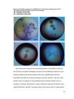
Figure 2-7 45º tilted view of wrinkled single crystal silicon ribbons using SEM 22
Figure 2-8 No debonding between silicon ribbon and PDMS at wave peaks 22
Figure 2-9 Sinusoidal profiles of wavy silicon ribbons 24
Figure 2-10 Micro-Raman measurements of silicon peak 24
Figure 2-11 Optical image of stretchable single crystal silicon n
p
diode on PDMS
substrate under applied strain 27
Figure 2-12 AFM images and relief profiles of wavy silicon ribbons 28
Figure 2-13 Silicon ribbon strain as function of applied strain. 28
xii
Figure 2-14 Current density vs. bias voltage for stretchable single crystal silicon
n
p
diode at different applied strains 29
Figure 3-1 Overview of Fabrication Process 32
Figure 3-2 Cross-sectional view of ICs 32
Figure 3-3 Schematic diagram for circuit preparation procedures 35
Figure 3-4 Fabrication Schematics of Ultrathin, Foldable and Stretchable Circuits 37
Figure 3-5 Circuits on carrier wafer 38
Figure 3-6 Ultrathin device on thin rod coated with PDMS 38
Figure 3-7 Thin and flexible feature of ultra-thin device: Si-CMOS inverters 39
Figure 3-8 Wavy ultrathin Si-CMOS inverters 40
Figure 3-9 Wavy Si-CMOS inverters formed 41
Figure 3-10 SEM of wavy Si-CMOS inverters 41
Figure 3-11 Wavy Si-CMOS inverters under tensile strains in
x
and
y
directions 42
Figure 3-12 Measured and simulated
n
(blue) and
p
(red) channel MOSFETs 44
Figure 3-13 Measured (red and black) and simulated (blue) transfer characteristics of
wavy inverters 44
Figure 3-14 Measured (solid circles) and simulated (open squares) inverter threshold
voltages for different applied strains (x and y directions) 45
Figure 3-15 IV curves for NMOS (left) and PMOS (right) at 0% strain; measurement
(solid lines) and simulation (dot lines) 45
Figure 3-16 Wavelength and amplitude measurement of wavy ultrathin devices 47
Figure 3-17 Optical image of array of stretchable 49
Figure 3-18 Time domain responses of an oscillator at different applied strains 50
Figure 3-19 Frequency domain responses of an oscillator at different applied strains
50
xiii
Figure 3-20 Circuit diagram of differential amplifier 51
Figure 3-21 Wavy differential amplifier in its as-fabricated state and under applied
strain in direction along red arrow 51
Figure 3-22 Output characteristics for various strain values 52
Figure 4-1 Wrinkled stiff thin film-compliant substrate system 54
Figure 4-2 Forces applied to an infinitesimal thin film plate element 56
Figure 4-3 Dimensionless stiffness
g
as function of
kH
(Huang et al. 2005) 63
Figure 4-4 Sensitivity of )21/()1(
2
ss
in terms of Poisson’s ratio 66
Figure 4-5 Critical membrane force
cr
N , vs. substrate/film thickness ratio (Huang et
al. 2005) 69
Figure 4-6 Illustration of fabrication procedures 70
Figure 4-7 Applied strain on wrinkled thin film silicon system 71
Figure 4-8 Comparison of experimental data and linear analytical prediction of
wavelength and amplitude of wavy silicon at prestrain=0.9%. 77
Figure 5-1 Optical micrographs of buckled Si ribbons on PDMS formed with various
prestrains (indicated on the right, as percentages) 79
Figure 5-2 Comparison of experimental data and linear analytical prediction of
wavelength and amplitude of wavy silicon 80
Figure 5-3 Fabrication process of stiff thin film-compliant substrate system 81
Figure 5-4 Buckled Si thin film and relaxed PDMS substrate of length
0
L (a) and
0
)1( L
applied
(b) under applied strain
applied
91
Figure 5-5 Comparison of wavelength and amplitude as function of prestrain 94
Figure 5-6 Comparison of membrane and peak strains as function of prestrain 96
xiv
Figure 5-7 Comparison of wavelength and amplitude as functions of
applied
with
pre
= 16.2% 99
Figure 5-8 Comparison of membrane and peak strains in film as function of
applied
with
pre
= 16.2% 100
Figure 5-9 Strechability and compressibility of buckled structures of Si on PDMS.
100
Figure 6-1 Applied load and traction force 107
Figure 6-2 Illustration of FE model configuration 112
Figure 6-3 Numerical simulation results for wrinkle patterns of silicon ribbon at
different substrate prestrain values. 113
Figure 6-4 Comparison between numerical and experimental results for wavelength
and amplitude at different prestrain 114
Figure 6-5 Illustration of FE model under applied strain 115
Figure 6-6 Schematic illustration of process for fabricating buckled single crystal
silicon ribbons (green) on PDMS (blue) substrate with edge effect 116
Figure 6-7 Wavy single crystal silicon ribbons on PDMS substrate. 117
Figure 6-8 Optical image of edge effect 117
Figure 6-9 Illustration of finite element model for edge effect 118
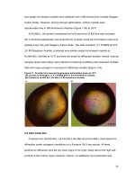
Figure 6-10 (a) Images and (b) linecuts of atomic force micrographs, and (c) finite
element results of buckled single crystal silicon ribbons on PDMS
substrate. 120
Figure 6-11 Wavelength and amplitude around center part of buckled silicon thin
film versus prestrain 121
Figure 6-12 Edge-effect length
edge
L versus prestrain 122
xv
Figure 6-13 Edge-effect length
edge
L versus modulus of substrate 123
Figure 6-14 Axial force in thin film 123
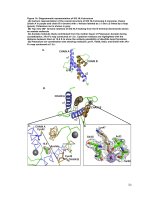
Figure 7-1 4-node quadrilateral element 128
Figure 7-2 Overview of wrinkling pattern 130
Figure 7-3 CAD drawing and FE mesh of integrated circuits and substrate 131
Figure 7-4 Finite element mesh of thin film 131
Figure 7-5 Strain-stress curve of PDMS (Choi and Rogers, 2003) 132
Figure 7-6 Finite element simulation process 134
Figure 7-7 Wrinkle forming due to substrate shrinking 137
Figure 7-8 Wavy pattern around etch hole at
pre
=3.9% 138
Figure 7-9 Comparison of wrinkle pattern at
pre
=3.9% 138
Figure 7-10 Comparison of wrinkle pattern observed through numerical simulation
(top) and experimental optical micrographs (bottom) 139
Figure 7-11 Comparison of wavelength and amplitude between numerical results and
experimental data for
pre
=3.9% 140
Figure 7-12 Maximum principle strain on top-plane of metal layer 142
Figure 7-13 Maximum principle strain on top-plane of Si layer 143
Figure 7-14 Von Mises Stress on top-plane of metal layer 144
Figure 7-15 Von Mises stress on top-plane of Si layer 145
xvi
List of Symbols
A and A
Amplitude
B Strain-displacement matrix
D Bending stiffness of plate
1
C and
2
C Material parameters
E Stress-strain matrix
IJ
E Green strain
f
E Young’s modulus of plate or thin film,
s
E Young’s modulus of substrate,
iJ
F Deformation gradient
N
F Force component
H
Substrate thickness
1
I Trace of left Cauchy-Green strain tensor
1
I First strain invariant
J
Elastic volume strain
L Stretched length of silicon ribbon
0
L Initial length of silicon ribbon
c
L Channel lengths
edge
L Edge-effect length
M Bending moment tensor
J
n Unit normal vector of surface
xvii
yixiwiviui
NNNNN ,,,, Shape functions
N
,
11
N ,
22
N ,
12
N Uniform stress and components in plane or thin film
cr
N Critical membrane force
c
R Radius of curvature at the peak or trough of wave
p
Stress component acting perpendicular to the plate,
t Thin film thickness
IJ
T 2
nd
Piola-Kirchoff stress
1
T
,
2
T
and
3
T Traction force components
D
T Temperature
U Strain energy
b
U Bending strain energy in plate or thin film
m
U
Membrane strain energy in plate or thin film
s
U Strain energy in the substrate
u , v or
1
u ,
2
u In-plane displacements
w Displacement perpendicular to plane or film deflections
i
w i -th eigenmode
W Channel width
b
W
Bending energy density in plate or thin film
m
W Membrane energy density in plate or thin film
s
W Strain energy density in substrate
1
x ,
2
x ,
3
x Cartesian coordinates
1
x
,
2
x
,
3
x
Cartesian coordinates after stretching
s
Coefficient of thermal expansion
xviii
Kronecker delta
if
if
,0
,1
and
0
11
,
0
22
,
0
12
Membrane strains components
applied
Applied strain
cr
Critical buckling strain
fracture
Fracture strain
pre
Prestrain
peak
Si
Strain at peak (or trough) in wavy silicon ribbon
Si
Silicon ribbon strain of wave
bending
Bending strain
s
Strain in substrate
f
Strain in thin film
mem
Membrane strain
peak
Peak strain
i
Scaling factor
eq
k Wave number
and
Wavelength
ourcot
Contour length of wave
f
Poisson’s ratio of the plate (i.e. thin film)
s
Poisson’s ratio of substrate
0
Prestress
cr
Critical buckling stress
Chapter 1 Introduction
1
Chapter One
Introduction
1.1 Background
Most electronic circuits are not stretchable because they come in the form of
rigid chips. Truly flexible circuits are made of organic semiconductors sprayed or
stamped onto plastic sheets. Currently organic semiconductors, although useful for
flexibility reasons, are slow for intensive computing tasks (Crone, et al., 2000).
Silicon or other high-speed inorganic semiconductors based on elastomeric substrates
are required for bendable and stretchable electronics systems (Yuan, et al., 2006).
This is why stretchable silicon was selected as one of the ten emerging technologies
by MIT Technology Review (Greene, 2006). Recently, a method has been found to
stretch crystal silicon (Khang, et al., 2006) and then fabricate it into integrated circuits
(Kim, et al., 2008). The work involved the use of single crystal silicon which is the
same type of silicon found in microprocessors. However, as with other crystal
materials, single crystal silicon does not stretch naturally. In order for it to be
bendable and stretchable, it has to be prepared as an ultrathin layer only a few
hundred nanometers thick on a bendable surface (Rogers, 2001). Instead of attaching
the single crystal silicon to a plastic substrate, the new method involves affixing
single crystal silicon in narrow strips onto a stretched, rubber-like polymer. When the
stretched polymer snaps back into its natural relaxed state, the silicon strips buckle,
but do not break, forming wrinkling waves that are ready to be stretched out again.
Recently this process has been extended to the fabrication of integrated circuits (Kim,
Chapter 1 Introduction
2
et al., 2008). The high performance, stretchable and foldable integrated circuits are
developed using the same approach. This inorganic electronic device is
systematically structured into aligned arrays of nanoribbons of single crystal silicon,
with ultrathin plastic and elastomeric substrates. The designs combine multilayer
layouts and ‘wavy’ structural configurations in silicon complementary logic gates,
ring oscillators and differential amplifiers. This is a different conceptual approach to
stretchable electronics. The desired mechanical properties are realized not through
new materials but instead through new structural configurations which are established
in the fabrication process. To understand the mechanism of this new structural
material, analytical and computational models are developed here to investigate the
mechanics characteristics in both single crystal silicon and integrated circuit systems.
The results show that this type of stiff thin film-compliant substrate system has good
potential of application for devices that require extreme mechanical deformations
during installation or usage.
The potential applications of circuitry made from the stretchable silicon and
integral circuits are vast, such as unusual types of displays, bendable monitors (Figure
1-1), stretchable display screens (Figure 1-2), and surgical gloves with sensors that
could read chemical levels in the blood and alert a surgeon to a problem, without
impairing the sense of touch (Figure 1-3). Stretchable electronics could allow a
prosthetic limb to use pressure or temperature cues to change its shape. More
applications can be found, for example, electronic eye cameras (Figure 1-4),
intelligent, wireless medical sensors, conformable skin sensors, structural health
monitoring devices and so on. Similar types of stiff thin film-compliant substrate
system also have many other emerging applications such as micro- and
Chapter 1 Introduction
3
nanoelectromechanical systems, tunable phase optics, force spectroscopy in cells,
biocompatible topographic matrices for cell alignment, high precision micro- and
nanometrology methods, and pattern formation for micro- and nanofabrication.
CRT Technology Active Matrix LCD Flexible FPD
> 50 years old > 25 years old Future
Time
Figure 1-1 Evolution of display technology (Crawford, 2005)
Figure 1-2 World’s first prototype of rollable display by Philips (Sinha, 2005)
Stretch
Chapter 1 Introduction
4
Figure 1-3 Smart micro sensor-based surgical glove (Lumelsky, 2001)
Figure 1-4 Electronic eye camera (Ko, et al., 2008)
A completely different conceptual approach to stretchable electronics emerges
from certain research on bendable inorganic electronics (Sun, et al., 2006a; Baca, et
al., 2008). Here, desired mechanical properties are realized not through new materials
but instead through new structural configurations of established materials. For
example, bendability can be achieved in intrinsically brittle materials, such as single-
crystalline silicon (Baca, et al., 2008) by implementing the materials in ultrathin
formats, nanowires (Duan, et al., 2003), nanoribbons, (Menard, et al., 2004),
Embedded
integrated circuits
RF transmit/receive
Sensors:
chemical,
optical,
thermal
fluidic
channels
Chapter 1 Introduction
5
nanomembranes (Ahn, et al., 2006) and, in some cases, in advanced neutral
mechanical plane designs (Kim, et al., 2008). An attractive feature of this strategy is
that it leads naturally to systems with improved electrical performance and reliability
comparable to those of wafer-scale electronics, far surpassing anything that is possible
with known organic active materials. For example, transistor devices with field effect
mobilities up to several hundred cm
2
V
-1
s
-1
in complementary circuits with bendability
to radii of curvature as small as 0.05mm can be achieved in this fashion (Ahn, et al.,
2006; Kim, et al., 2008). The extension to stretchable electrics is remarkably
straightforward: ultrathin material structures formed into ‘wavy’ or buckled
geometries offer stretchability with a physical structure similar to an accordion
bellows, without inducing significant strains in the materials themselves (Baca, et al.,
2008; Sun, et al., 2006b). This approach has recently been used to create stretchable
conductors, transistors, diodes, photodetectors, circuits of various types and even fully
integrated systems such as hemispherical electronic eye cameras (Ko, et al., 2008). A
separate body of work uses material structures in a different way to yield a similar
outcome. Here, open meshes (Someya, et al., 2004) constructed in bendable materials
provide large, reversible levels of deformability for strains applied along certain axes,
are used in systems such as sensitive robotic skins (Dinyari, et al., 2008). Cantilever-
spring structures in silicon, exploit related examples of device level demonstrations of
them. Dinyari, et al. (2008) and Hung, et al. (2004) conclude it with some
perspectives on future research opportunities.
Stretchable electronics represents a much more challenging class of system,
and is of interest for applications where circuits must be wrapped conformally around
complex curvilinear shapes or integrated with biological tissues in ways that are
Chapter 1 Introduction
6
impossible using devices that offer only simple bendability. The new type of
stretchable electronic system studied here is impressive because it works with single-
crystal silicon which is made out of standard, high performance silicon. The fully
stretchable form of single-crystal silicon with micron-sized, wave-like geometries can
be used to build high-performance electronic devices on rubber substrates. Figure 1-5
schematically illustrates one method for integrating thin films of high quality
electronic materials with elastomeric substrates for stretchable electronics. The first
step (Figure 1-5a) involves fabrication of thin elements of single crystal silicon or
completes integrated devices (transistors, diodes, etc.) by conventional lithographic
processing. After this process, the thin film structures are supported by, but not
bonded to, the underlying wafer. Contact between the prestrained, compliant
substrate and the stiff thin film, leads to bonding between these materials (Figure 1-5b
and Figure 1-5c). When the substrate is peeled back, with the film bonded to its
surface, and then the prestrain released, causes the substrate to relax back to its
unstrained state. This relaxation leads to the spontaneous formation of well-
controlled, highly periodic, stretchable wave structures in the thin film (Figure 1-5d)
and the region of near the top surface of substrate.
Chapter 1 Introduction
7
Figure 1-5 Schematic illustration of method for integrating thin films of high quality
electronic materials (Greene, K., 2006)
The same method can also be applied to high performance, single crystalline
silicon complementary metal oxide semiconductor (Si-CMOS) integrated circuits (ICs)
to make them into reversibly foldable and stretchable systems. These systems
combine high quality electronic materials, such as aligned arrays of silicon
nanoribbons, with ultrathin film and elastomeric substrates exhibiting ‘wavy’
structural layouts. These approaches are important not only for the Si-CMOS circuits
that they enable, but also for their straightforward scalability to much more highly
(a)
(b)
(c)
(d)