An adaptive algorithm for direct conversion receivers architecture and performance analysis
Bạn đang xem bản rút gọn của tài liệu. Xem và tải ngay bản đầy đủ của tài liệu tại đây (543.3 KB, 84 trang )
AN ADAPTIVE ALGORITHM FOR DIRECT
CONVERSION RECEIVERS: ARCHITECTURE AND
PERFORMANCE ANALYSIS
CAO MINGZHENG
NATIONAL UNIVERSITY OF SINGAPORE
2005
AN ADAPTIVE ALGORITHM FOR DIRECT
CONVERSION RECEIVERS: ARCHITECTURE AND
PERFORMANCE ANALYSIS
CAO MINGZHENG
(B. Eng)
A THESIS SUBMITTED
FOR THE DEGREE OF MASTER OF ENGINEERING
DEPARTMENT OF ELECTRICAL AND COMPUTER ENGINEERING
NATIONAL UNIVERSITY OF SINGAPORE
2005
ACKNOWLEDGEMENTS
I would like to express my utmost appreciation to both of my supervisors, Dr. Zheng
Yuanjin and Prof. Hari Krishna Garg, for their invaluable guidance, continuing
support and constructive suggestions throughout my research and study in the
National University of Singapore and the Institute of Microelectronics. Their deep
insight and wide knowledge have helped me out at the various phase of my research.
It has been an enjoyable and a cultivating experience working with them.
Next, I would like to thank my great colleagues in ECE-I2R lab for all their helps and
for making my study life in NUS so wonderful.
Last but not least, I would also like to thank my family members who have always
been the best supports in my life.
i
SUMMARY
An adaptive algorithm is proposed in this thesis to remove in-phase and quadrature
(I/Q) mismatch, direct current (DC) offsets, flicker noise and inter-symbol
interference (ISI) simultaneously in a direct conversion receiver (DCR). I/Q mismatch
is cancelled by a real valued adaptive mismatch canceller and DC offsets are removed
with one complex tap. In addition, flicker noise is modeled as a complex
autoregressive (AR) random process so the system to be identified transforms to an
Auto Regressive with eXternal input (ARX) model. After estimating the coefficients
in the model during training period, the desired signal can be estimated by using
decision feedback method. To accelerate the convergence of the algorithm and to
mitigate the interactions among the adaptations of the different groups of the taps of
the filters, an internal iterative algorithm is introduced. Moreover, the analysis of the
convergence in the mean of the taps of the proposed filters is given. Simulation results
are provided to verify the superior performance of the proposed algorithm.
ii
CONTENTS
ACKNOWLEDGEMENTS
i
SUMMARY
ii
LIST OF ABBREVIATIONS
v
LIST OF SYMBOLS
vii
LIST OF FIGURES
xii
CHAPTER 1 INTRODUCTION
1.1
1.2
1.3
1.4
1.5
1.6
1.7
Outline
Background
Challenges of DCR Design
Previous Works on DCR Design
Contributions of Thesis
Organization of Thesis
Summary
1
1
4
7
8
8
9
CHAPTER 2 RECEIVED SIGNAL MODEL
2.1
2.2
2.3
2.4
2.5
2.6
Outline
Introduction
DC Offsets Model
Flicker Noise Model
I/Q Mismatch Model
Summary
11
11
12
18
20
21
iii
CHAPTER 3 THE ADAPTIVE FILTERS AND ALGORITHM
3.1
3.2
3.3
3.4
3.5
3.6
3.7
Outline
Introduction
Architecture of the Adaptive Filters
Adaptive Algorithm for Distortion Mitigation
Internal Iterative Algorithm
Implementation Complexity
Summary
23
23
25
26
32
36
36
CHAPTER 4 CONVERGENCE ANALYSIS
4.1
4.2
4.3
Outline
Convergence Analysis
Summary
38
38
50
CHAPTER 5 SIMULATION RESULTS
5.1
5.2
5.3
5.4
5.5
5.6
5.7
5.8
5.9
Outline
Introduction
Performance of Mismatch Canceller
Performance of DC Offsets Canceller
Performance of Mismatch Canceller and DC Offsets Canceller
Performance of CDFE
Performance of the Internal Iterations
Comprehensive Performance of the Proposed Algorithm
Summary
51
51
52
53
55
57
60
61
64
CHAPTER 6 CONCLUSIONS AND FUTURE WORK
6.1
6.2
Conclusions
Future Work
65
66
REFERENCES
68
LIST OF PUBLICATIONS
70
iv
LIST OF ABBREVIATIONS
AC:
alternate current
ADC:
analog-to-digital converter
AR:
Auto Regressive
ARX:
Auto Regressive with eXternal input
AWGN:
additive white Gaussian noise
BER:
bit error rate
BPSK:
binary phase shift keying
CDFE:
complex decision feedback equalizer
CFFE:
complex feed forward equalizer
DC:
direct current
DCR:
direct conversion receiver
DSP:
digital signal processing
FIR:
finite-impulse response
I:
in-phase
IC:
integrated circuit
IF:
intermediate frequency
I/Q :
in-phase and quadrature
ISI:
inter-symbol interference
LE:
linear equalizer
v
LMS:
least mean square
LNA:
low noise amplifier
LO:
local oscillator
LPF:
low pass filter
MMSE:
minimum mean-square-error
MOS:
metal oxide semiconductor
MSE:
mean-square-error
PSD:
power spectral density
Q:
quadrature
QPSK:
quadrature phase shift keying
RF:
radio frequency
SDR:
signal to constant DC offset ratio/signal to varying and constant DC
offsets power ratio
SFR:
signal to flicker noise power ratio
SNR:
signal to noise power ratio
16 QAM:
16 quadrature amplitude modulation
vi
LIST OF SYMBOLS
{ai } :
coefficients of AR model
{aˆi } :
estimated coefficients of
A( z ) :
see (2-23)
{bi } :
see (3-8)
{bˆ } :
estimated coefficients of
B(z) :
A( z ) H ( z )
c (t ) :
channel response in time domain
C( f ):
channel response in frequency domain
d (t ) :
varying DC offset
d (t ) :
constant DC offset
e (n) :
filtering error signal
f (t ) :
flicker noise
fc :
carrier frequency
fs :
ADC sampling rate
f0 :
offset frequency away from f c
F (z) :
z − transform of f ( n )
g (t ) :
pulse with a band-limited frequency response characteristic
G( f ) :
g ( t ) in frequency domain
i
{ai }
{bi }
vii
h (t ) :
convolution of g ( t ) and c ( t )
{hi } :
coefficients of the combined channel discrete time impulse response
H (z) :
z − transform of h ( n )
k1 :
order of the CFFE taps
k2 :
order of the CDFE taps
m (n) :
equivalent transceiver I/Q mismatch induced signal
mˆ 1kj ( n ) :
see (4-31)
{mi } :
taps of I/Q mismatch canceller
{mio } :
optimum values of
M:
mismatch matrix
ˆ ( n) :
M
1
k1 × k1 matrix with the elements of mˆ 1kj ( n )
n:
discrete time index
n (n) :
additive white Gaussian noise
n′ ( n ) :
white Gaussian noise
Na −1:
order of AR model
Nh :
order of channel response
N:
total number of internal iterations
Pˆ ( n ) :
⎛Y ′(n) t* (n) ⎞
⎜⎜
⎟⎟
*
⎝T ′(n) t (n) ⎠
P:
E ⎡⎣ Pˆ ( n ) ⎤⎦
Rˆ ( n ) :
⎡Y ′ ( n ) ⎤ H
H
⎢ ′ ⎥ ⎡⎣Y ′ ( n ) T ′ ( n ) ⎤⎦
T
n
⎣ ( )⎦
R:
E ⎡⎣ Rˆ ( n ) ⎤⎦
{mi }
viii
Rˆ T ′ ( n ) :
T ′ ( n ) T ′H ( n )
Rˆ XI ( n ) :
X I ( n ) X IH ( n )
RXI :
E ⎡⎣ Rˆ XI ( n ) ⎤⎦
Rˆ XQ ( n ) :
X Q ( n ) X QH ( n )
RXQ :
E ⎡⎣ Rˆ XQ ( n ) ⎤⎦
Rˆ Y ′ ( n ) :
Y ′ ( n ) Y ′H ( n )
s (t ) :
equivalent low-pass interference signal
s p (t ) :
band-pass interference signal
t (m) :
discrete information-bearing sequence of symbols
t (n) :
training sequence
tˆ ( n ) :
estimated transmitted sequence
T (z) :
z − transform of t ( n )
T ′(n) :
⎡⎣ t * ( n − 1) t * ( n − 2 ) … t * ( n − N b + 1) ⎤⎦
u (t ) :
LO signal
u (t ) :
LO signal contaminated by the leakage signal
v (n) :
innovation of AR model
v (t ) :
equivalent low-pass transmitted signal
V ( z) :
z − transform of v ( n )
w* :
tap of DC canceller
{w } :
*
j
taps of CFFE
{w } :
taps of CDFE
W ( n) :
⎡⎣ w * ( n ) w * ( n − 1)
*
k
w * ( n − N a + 1) ⎤⎦
H
T
ix
W ( n) :
⎡⎣ w0* ( n ) w1* ( n )
w *Na −1 ( n ) ⎤⎦
H
W ( n) :
⎡⎣ w1* ( n ) w2* ( n )
w *Nb −1 ( n ) ⎤⎦
H
x (n) :
digitalized baseband signal after the ADC to be processed by the
proposed adaptive algorithm
x (t ) :
equivalent low-pass received signal
xp (t ) :
band-pass received signal
xp (t ) :
received signal comtaminated by the interference signal
x′ ( t ) :
received signal corrupted by ISI and two kinds of DC offsets
x (t ) :
demodulated baseband signal corrupted by ISI, two kinds of DC offsets
and flicker nosie before the ADC
x ( n) :
samples of x ( t )
xˆ ( n ) :
received signal with mismatch cancelled
x′ ( n ) :
signal with mismatch and DC offsets cancelled
X (n) :
⎡⎣ x * ( n )
X I ( n) :
real parts of X ( n )
XQ (n) :
imaginary parts of X ( n )
y (n) :
output of mismatch canceller
y′ ( n ) :
received signal with mismatch and DC offsets cancelled
Y ′(n) :
⎡⎣ y′* ( n )
Y ′( z) :
z − transform of y′ ( n )
z (n) :
output signal of the proposed adaptive filter
α:
amplitude gain of the I channel
x* ( n − 1) … x * ( n − N a + 1) ⎤⎦
H
y′* ( n − 1) … y′* ( n − N a + 1) ⎤⎦
H
x
β:
amplitude gain of the Q channel
φ:
phase splitter mismatch
*:
complex conjugation
μb :
step size for adjusting
μd :
step size for adjusting w
μf :
step size for adjusting
{w }
μm :
step size for adjusting
{mi }
λmax :
maximum eigenvalue of R
ξˆ ( n ) :
e (n)
{w }
*
k
*
j
2
xi
LIST OF FIGURES
Figure 1-1
Physical model of super heterodyne receiver
2
Figure 1-2
Image rejection and adjacent channel suppression
3
Figure 1-3
Physical model of DCR
4
Figure 1-4
Self-mixing of (a) LO. (b) Interferers
5
Figure 1-5
PSD of flicker noise
6
Figure 1-6
Direct conversion architecture
7
Figure 3-1
Signal flow and the proposed adaptive filter
26
Figure 5-1
BER performance of the mismatch canceller
53
Figure 5-2
BER performance of the DC offsets canceller
54
Figure 5-3
BER performance of BPSK
56
Figure 5-4
BER performance of QPSK
56
Figure 5-5
BER performance of 16 QAM
57
Figure 5-6
PSD of flicker noise and transmitted signal
59
Figure 5-7
BER performance of CDFE
59
Figure 5-8
Learning curve of the proposed algorithm without and with
internal iterations
61
Figure 5-9
Comprehensive BER performance of BPSK
62
Figure 5-10
Comprehensive BER performance of QPSK
63
Figure 5-11
Comprehensive BER performance of 16QAM
63
xii
CHAPTER 1
INTRODUCTION
1.1
Outline
In this chapter the motivations, the challenges and the previous works of the topics
involved in the thesis are given, followed by the contributions and the organization of the
thesis. The background is introduced in Section 1.2. Then the challenges of the direct
conversion receiver (DCR) design and the previous works on DCR design are given in
Section 1.3 and Section 1.4, respectively. In addition, the contributions of the thesis are
given in Section 1.5. Moreover, the organization of the thesis is given in Section 1.6.
1.2
Background
Nearly all existing radio receivers are designed based on a super heterodyne architecture.
They filter the received radio frequency (RF) signal and convert it to a lower intermediate
frequency (IF) by mixing with an offset local oscillator (LO1) as shown in Fig. 1-1 [1].
The IF filter is used to suppress out-of-channel interferers, performing channel selection.
During the down conversion of the signal from RF to IF, an unwanted signal which is
situated at an intermediate frequency above the LO1 frequency is also translated to the IF.
This undesired signal is called image signal and should be removed. The principal issue
1
in super heterodyne receivers is the tradeoff between the image signal rejection and the
adjacent channel suppression [2].
ADC
RF
filter
IF
filter
D
S
P
ADC
LO1
( fcarrier − f IF )
LO2 ( f IF )
Fig. 1-1: Physical model of super heterodyne receiver.
As shown in Fig. 1-2, if the amplitude of the IF signal is high, the image is greatly
attenuated but the nearby interferers remain at significant levels. On the contrary, if the
amplitude of the IF signal is low, the interferers are suppressed but the image corrupts the
down converted signal significantly. Consequently, both the image reject filter and the IF
filter required highly selective transfer functions that are impractical in today’s integrated
circuit (IC) technologies. In practice, most systems utilize dual-conversion (two IF’s) or a
triple-conversion (three IF’s) in order to achieve an acceptable compromise between the
two rejections, which is at the expense of added receiver complexity and size [1] [2]. In
addition, because the image reject filter is placed off-chip, a 50- Ω load is needed for the
low noise amplifier (LNA) before the image reject filter. This adds another dimension to
the tradeoffs among noise, linearity, gain, and power dissipation of the amplifier [2].
2
Desired
Channel
Image
Reject Filter
Image
Channel
Select Filter
Interferer
ω1
2ωIF
ωim ω
0
ω
ωim
ω
0
2ωIF
ωIF
ωIF
ω
ω
Fig. 1-2: Image rejection and adjacent channel suppression.
As shown in Fig. 1-3, If the IF signal is designed to be at frequency zero, it is called
direct conversion [1] [2]. Compared to the receiver based on a super heterodyne
architecture, the direct conversion receiver (DCR) has superior advantages in power
dissipation, size and cost because in DCR no image reject filter is required and all IF
analog components are eliminated [1] [2]. But DCR is rarely used so far due to some
issues such as in-phase and quadrature (I/Q) mismatch, direct current (DC) offsets,
even-order distortion and flicker noise [1] - [4]. Among these issues, DC offsets and
flicker noise are generally considered more serious and challenging to the designers [2]
[5]. In addition, the mismatch between the in-phase (I) and quadrature (Q) channel
always exists [6]. Consequently, the methods to cancel I/Q mismatch, DC offsets and
flicker noise cancellation are more frequently discussed than other issues.
3
RF
filter
baseband
filter
ADC
baseband
filter
ADC
D
S
P
LO ( f carrier )
Fig. 1-3 Physical model of DCR.
1.3
Challenges of DCR Design
In a DCR, an offset voltage may appear in the signal spectrum at DC. This offset voltage
value dominates the signal strength by as much as 50~100 times in amplitude and, if not
removed, may substantially degrade the bit-error probability [2]. As the receiver shown in
Fig. 1-4, where the low pass filter (LPF) is followed by an amplifier and an
analog-to-digital converter (ADC), there are two phenomena causing DC offsets. Because
the isolation between the LO port and the inputs of the mixer and the LNA is not perfect,
there is a finite amount of feedthrough from the LO port to points A and B [1]. The
leakage signal appearing at the inputs of the LNA and the mixer is now mixed with the
LO signal, which is called self-mixing, thus producing a DC component at point C as
shown in Fig. 1-4(a). Similarly, DC offset occurs if a large interferer leaks from the LNA
or mixer input to the LO port and is multiplied by itself [1], as shown in Fig. 1-4(b). In
addition, DC offset also can be caused by the transistor mismatch in the signal path, but
DC offsets caused by this reason and the self-mixing of the interferer leakage can be
4
reduced to some extent by careful front-end receiver design together [7]. The
comprehensive DC offsets caused by all these reasons are time-varying.
LNA
A
C
B
LO Leakage
Amplifier
ADC
LPF
LO
(a)
LNA
A
C
B
Interferer
Leakage
LPF
Amplifier
ADC
LO
(b)
Fig. 1-4 Self-mixing of (a) LO. and (b) Interferers.
The flicker noise, also known as 1/f noise or pink noise, is an intrinsic noise phenomenon
found in semiconductor devices. As the term “1/f” suggests, the noise is characterized by
a power spectral density (PSD) that is inversely proportional to frequency, as shown in
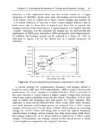
Fig. 1-5. In a DCR, since the downconverted spectrum is located around zero frequency,
the 1/f noise of devices has a profound effect on the signal, a severe problem in metal
oxide semiconductor (MOS) implementations. For example, in typical submicron MOS
technologies, the total flicker noise power in a bandwidth from 10 Hz to 200 kHz can
increase the noise power by 16.9 dB [1].
5
-60
-65
PSD of flicker noise (dB)
-70
-75
-80
-85
-90
-95
-100
0
0.5
1
1.5
2
2.5
3
Frequency (MHz)
3.5
4
4.5
5
Fig. 1-5 PSD of flicker noise.
As shown in Fig. 1-6, for most phase and frequency modulation schemes, a DCR must
incorporate quadrature downconversion, which requires shifting the LO output by 90o .
Due to the finite tolerances of capacitor and resistor values used to implement the analog
components [6], the errors in the nominally 90o phase shift and mismatches between the
amplitudes of the I and Q signals corrupt the downconverted signal constellation [1]. The
imbalance between the amplitudes of I and Q channels and the phase shift error are
totally called I/Q mismatch.
6
LPF
LNA
ω0
ω
I
sin ω0
cos ω0
0
LPF
ω
Q
Fig. 1-6 Direct conversion architecture.
1.4
Previous Works on DCR Design
Many papers have proposed various methods to solve DC offsets and flicker noise [2] [3]
[7] [8]. In [2] the DC offset is removed by employing an alternate current (AC) coupling
which may distort the signals’ DC components due to its high corner frequency [1] [8]; in
addition, the flicker noise is regarded as equivalent in its effect to inter-symbol
interference (ISI) and mitigated only by employing a finite-impulse response (FIR)
minimum mean-square-error linear equalizer (MMSE-LE); moreover, it is difficult to
design a suitable AC coupling because the exact 1/f roll-off frequency is unknown in
practice. In [7] the varying DC component is not considered when making joint
estimation of the DC offset and the radio channel. In [8] an extra averaging circuit is
needed to do long-term averaging of the baseband signal to remove the DC offsets by
subtracting the estimated DC value, which will increase the cost and the size of the
receivers.
7
1.5
Contributions of the Thesis
In this thesis, a novel method to estimate the transmitted signal corrupted by ISI, I/Q
mismatch, DC offsets and flicker noise is proposed. A real valued adaptive mismatch
canceller is employed to cancel I/Q mismatch and the varying DC offsets are removed by
one complex tap simultaneously [9] [3]. In addition, the flicker noise is modeled as a
complex auto regressive (AR) random process, so the system transforms to an Auto
Regressive with eXternal input (ARX) model [10]. By estimating the coefficients of the
model during training period, the desired signal then can be estimated by decision
feedback method. To accelerate the convergence of the algorithm, an internal iterative
algorithm is introduced [9]. Moreover, the analysis of the convergence in the mean of the
taps of the proposed algorithm is given. Simulation results are provided to verify the
superior performance of the proposed algorithm
1.6
Organization of the Thesis
In Chapter 2, the received signal model which is the transmitted signal corrupted by
channel ISI, I/Q mismatch, DC offsets and flicker noise is given. In Chapter 3, the
architecture of the proposed adaptive filters is illustrated and the detailed algorithm to
cancel all the previously mentioned distortions is derived.
To accelerate the
convergence of the algorithm, an internal iterative algorithm is introduced. In Chapter 4,
8
the convergence analysis in the mean of the taps is discussed. In Chapter 5, simulation
results are illustrated to verify the proposed algorithm. Finally, conclusions and future
work are given in Chapter 6.
1.7
Summary
Nearly all existing radio receivers are designed based on a super heterodyne architecture.
The principal issue in super heterodyne receivers is the tradeoff between the image signal
rejection and the adjacent channel suppression, which makes the implementation
complicated. Compared to the receiver based on a super heterodyne architecture, the
DCR has superior advantages in power dissipation, size and cost because in DCR no
image reject filter is required and all IF analog components are eliminated. But DCR is
rarely used so far due to some issues such as I/Q mismatch, DC offsets, even-order
distortion and flicker noise. In DCR design, the methods to cancel I/Q mismatch, DC
offsets and flicker noise cancellation are more frequently discussed than other issues.
There are two phenomena causing DC offsets. One is caused by self-mixing of LO and is
regarded as a constant. The other is caused by self-mixing of interferers and is time
varying. The flicker noise is an intrinsic noise phenomenon found in semiconductor
devices and is characterized by a PSD that is inversely proportional to frequency. The I/Q
mismatch is caused by the imbalance between the amplitudes of I and Q channels and the
phase shift error. In this thesis, a novel method to estimate the transmitted signal distorted
by ISI, I/Q mismatch, DC offsets and flicker noise is proposed. In the following chapters,
9
the architecture of the proposed adaptive filters, the detailed algorithm to cancel all the
previously mentioned distortions, the convergence analysis, the simulation results and the
conclusions are given.
10
CHAPTER 2
RECEIVED SIGNAL MODEL
2.1
Outline
In this chapter the received signal model is given. In Section 2.2 the background to model
the DC offsets, flicker noise and I/Q mismatch is discussed. Then the DC offsets model,
flicker noise model and I/Q mismatch model are given in Section 2.3, Section 2.4 and
Section 2.5, respectively.
2.2
Introduction
As mentioned in Section 1.2, in DCR design, DC offsets and flicker noise are generally
considered more serious and challenging to the designers [2] [5]. In addition, the
mismatch between I and Q channel always exists [6]. So this thesis focuses on I/Q
mismatch, DC offsets and flicker noise cancellation.
As discussed in Section 1.3, there are two kinds of DC offsets. One is caused by
self-mixing of LO and the other is caused by self-mixing of the interferences. The DC
offset caused by LO changes slowly, so it is can be regarded as constant value over a
packet duration. But the self-mixing caused by the signal leakage from RF input signal to
11