DSpace at VNU: Using high algebra to design frequency divider include hazard
Bạn đang xem bản rút gọn của tài liệu. Xem và tải ngay bản đầy đủ của tài liệu tại đây (3.83 MB, 8 trang )
V N Ư Journal o f Science, M athem atics - Physics 24 (2008) 163-170
U sing high algebra to design frequency divider include hazard
Nguyen Quy Thuong*
VNƯ, 144 Xuan Thuy, Cau Giay, Hanoi, Vietnam
R eceived 8 July 2008; received in revised form 8 A u g u st 2008
A b s tra c t. N o rm ally the frequency divider designed by B oole algebra an d to design a frequency
div id er w ith any divide factor, we h ave to repeat all over again every d e sig n step as the sam e. So
to avoid o f w asting tim e and m oney, instead o f using traditional B oole alg eb ra in digital technical
w e replace it by m athem atical m odels in high algebra. A nd becau se o f that we can design
frequency dividers use Computer.
1. Modeling of function circuit
Follow [1,2] show that with one frequency divider has 4/3 factor we need 2 flip flop (FF) and
NAND gates to control chain so that with 4 input impulse we ju st have only 3 output impulse.
How ever using NAND gate to control output impulse likes this, it ju st right in some cases. So to
design frequency divider with any divider K factor (meaning with any input and output im pulse follow
request o f user) w e use O R gate to control output impulse.
Investigate, for example, the input static D and output static Q o f D FF in asynchronous
Divider, real binary, 3 input, c ivide factor K= 7/6)
m
F ig 1. D iag ram im pulse o f frequency divider 7/6.
Q1
8
Qi
D
■c m
R ca
8
D
CO-
-c
R
m
02
08
m
oi
&
08
&
04
02
Fig. 2. F requency divider 7/6 execute follow d iag ram im pulse F ig. 1
E-mail:
163
164
N.Q . T h u o n g / V N U Jo u rn a l o f Science, M athem atics - P hysics 24 (2008) Ỉ 6 3 -170
From circuit o f frequency divider picture 2 and impulse diagram Fig. 1, we realize that in the time
o f first impulse to sixth impulse have at lease one o f three input signal o f NAND gate G1 receive 0, so
output o f G3 {G1,G2} - 1. In this time frequency divider will receive 6 impulses from output
gate G4.
To impulse 7 output o f gate G2 {Q l, Q2, Q3} receive level 0 and because o f that G3 - 0,follow G4
receive level 0 too. So because o f OR gate G2, we conữolled output frequency divider is M 6 .
From Fig. 2 w e have circuit function o f frequency divider 7/6
k
If frequency divider has
8 / 6 , 9/6, ...x/6
- 1 = q ,q , q M + Q 2 ^ Q ^ ) - c
o
( 1)
K - — w ith any X input impulse, mean any n Flip Flop , example
6
then discover more output 0 4 , Qs ....o f FF4, F F 5 ... from OR input. Now frequency
divider with K = — have circuit function:
6
K = l = Ổ,Ổ2Ổ3 ( Ỡ + a + a ) - ổ 4 ổ 4 - c
(2)
o
Obvious, because o f OR gates then after output impulse position M, circuit will reset.
Same as above we have Table 1, X is number o f input impulse, M is num ber output impulse and
K is a divider factor.
Table 1. Circuit function of frequency divider with any divide factor K
=
—
,X
M
M is number output impulse, here M € [4,31
K=
^
M
Function
X/ A
QiQiQi {QiQ} + Q:\)Qi
X/ b
Q,Q,Q, (Q, + Q,)Q,
X / Of
Q,Q,Q, (g, + Q , + Q,)Q,
X /Ĩ
QiQzQiiQi
X/ s
QrQzQiiQi {Q1Q2Q3 + Qá)Qh
X/ 9
X /1 0
X / 11
{Q-iQ-Ằ + Q.ỉ)Qõ
Q\Q-2Q:iQA{Qi + Q-2)Q:ì + Q^ÌQ->
+
Q.ị)Qr,
x/12
Q^Q2QAiQ.Q2+Qi)Q.
x /1 3
QiQzQiQiiQi + Q.i + *34)^5
x /u
Q\Q2Q:ìQa{Qì + Qi + Q.ị + QJQs
x/15
X
/ 16
x/17
Qì Q-1QaQ\ Ọ5{Q‘iQ:\Q\ + ộó )Qcy
x/is
Q^Q2Q.QAAQ.^Q2)Q- sQ ,+ Q ,Q ,
is number of input impulse,
N.Q. T ỉm o n g / VN U J o u rn a l o f Science, M athem atics - P hysics 24 (2008) 1 6 3 -1 70
X /1 6
Q,Q,Q,QMQ.Q2Q.Q.+Qr,)Q.
x/17
q ,q , q , Q
x /1 8
Q,Q,Q,Q,Q,[(Q, + Q,)Q,Q, + Q , u
x/l9
Q M A A Q Á Q A + QủQ>,
A Á Q A A + Q rM
x/20
+ Q,)Qi + Q M
x/21
Q M Q M \iQ .+ Q :M + Q M
x/22
Q,Q,Q,Q„QJ(Q, + Q, + Q JQ , +
x/23
Q m m x Q .+ Q M
x/24
Q m . Q M Q m . Q . + Qủ
x/25
Q m . Q M Q A > + Q.^ + Q r M
x/26
Q A Q .Q M Ả iQ . + Q M +
x/27
Q ^ Q A Q M Q , + Q.^ + QủQ.
x/28
Q m A M Q A + Q. + a . + Q r M
x/29
Q m .Q A iQ .+ Q .)Q .+ Q r M
x /m
x /-i\
165
+ Q r ,U
+ Q 2 + Q, + Q . + QÙ Q.
Q^Q,Q,QA,Q.
From table 1 and com m ent above, we realize circuit function o f frequency divider with any
divider factor have 2 forms:
form 1;
K =
Q Q -Q . . ■Q„ =
/ -I
(3)
A part o f function left over in brackets (Table 1) is a second form :
form 2:
K l = y + Q„
W e need to define function y.
2. Define y o f circuit function
From circuit function (Table 1) we found the form 2 (Table 2)
(4)
166
N.Q. T h u o n g / VN U J o u rn a l o f Science, M athem atics - P hysics 24 (2008) 163-170
X
Table 2. Circuit function form 2 apply to frequency divider with divide factor K = — , n is number of Flipflop
M
F is frequency appear circuit function in proportion to K factor, Fj, e\ 0,1,2,3 I is a basic frequency to show
circulate of circuit function
Flipflop n
B asis
frequenz F b
F requenz F
K = x/M
F o rm 2
0
0
x/4
Q.Q.
+ Q;,
1
1
x/5
Q.
+ Q:i
2
2
x/6
Q\ + Q i
+ Ql
3
3
3
x/7
1
+ Q;i
4
0
0
x/8
■a> + Q,,
1
1
x/9
Qi + Qi
2
2
x/10
3
3
x/11
Ồ.....................
4
x/12
1
5
x/13
Q.
2
6
x/14
Qi + Qi
+ Qi + Q,\
3
7
x/15
1
+ Qi + Qi
0
0
x/16
Q.Q,
1
1
x/17
■
2
2
x/18
■Q:iQ\ +
‘i ......................... 3
x/19
1
0
4
x/20
(Q.Q.
1
5
x/21
(Q.
+ Q .)Q ,+ Q .
2
6
x/22
(Q. + Q,
+ Qi )<3d + Q-,
7
x/23
(1
+ Q| )Q4 + Q-,
0
8
x/24
Q.Q,
1
9
x/25
Q,
2
10
x/26
3
11
x/27
1
■Qi + Qi +
0
12
x/28
Q.Q,
+ Qi + Qi + Qt,
1
13
x/29
Q,
+ Q:k + Q.| + Qõ
2
14
x/30
Q, + Qj
+ Q.I + Q,1 + Qs
3
15
x/31
1
+ Q:, + Q, + Ọ.
•5 .......................
5
(Q, + Q .)
1
•Q| + Qi
•Ộ.1 + + Q:i + Q.I
(Q. + Q J
+ Q, +
•Q.Ọ , +Qr,
+ Q,
•Q:,Q, + a ,
+ Qi )Q.| +
■Q:i + Qi + Qr,
■
Qi + Q a + Qĩ,
■Qi + Q\ + Qr>
N.Q. T h u o ĩig / VN U J o u rn a l o f Science. M athem atics - P hysics 24 (2008) 163-170
67
From table 2 we realize: circuit function need to find m atching with each divide K factor
depend on n and F, also we can build the relationship betw een n, F, M
M = 4.2"-' + F
(5)
F = M - 4.2"-^
(6 )
Provide: - n is a num ber o f Flipflop take parts o f divider.
F is frequency appear o f circuit function in each frequency divider n- FF, follo
circulate from 0 to 2 " - 1
Also from table 2 w e realize a part o f circuit function o f frequency divider having output
impulse M from 4 to 7(in proportion to n
= 3, F = (0, 1, 2, 3))is ju st a part o f circuit function have
output im pulse M > 8 ( this is Q1Q2; Q2 ; Qi + Q2 ; !)• So we take this circuit function make a basic
form and symbol as y „=3 to define circuit function o f all other frequency divider:
Ẩ, i f F = 0, 2 '" ' - 1
ifF =
A
(7)
2''-' - 1
In which:
0 if F = 0
Ai = (Q | + Ỉ,) . Qĩ
with
=
(8)
1 ifF = r~ --\
It call Product Form
0 if F ^ r - ^
It call Sum Form
From ( 8 ) and (9) and consider Qi
(9)
w ith ặ =
A2 = (Q, +^) + Q2
1 if F = r~ ' -1
= K ị we have:
(10)
In which:
0 i f F = [0, 2 ”- ' - 1
/? =
\ if
n-2
(11)
2"-' - 1
(12)
+a
From table 2 show that circuit function in proportion to n = 4, w hen Frequency Fb = (0 ,...3 ) =
0 ... 2"'^ - 1] then circuit function has also product form and sum form as y „=3 and this
circuit
function include circuit function o f y„=3- W e call this circuit function form is Yn=4
Thus:
= (Ỡ 3 + ụ ' ) y „.3 + ^ 3
(13)
0 ỉ/ F = [o, 2 "'" - 1 '
ụ/ = <
(14)
Thus
In which:
1 i f F = [2''--, 2"-' - 1
2
Thus:
Same as let n = 5 w ith F b = (0,...7) = [0,
(15)
and n = 6 w ith F b = (0,...15) = [ 0 , 2 " ^ -1]
y„-.s-(Q .+ ^)y.^4+ ^04
w ith :
1 =
0 i f F = 0, 2 "“' - 1'
1 i f F = 2 " -', 2 '" '- - 1'
(16)
(1 7 )
168
N.Q. T h u o n g / VN U J o u rn a l o f Science, M athem atics - P hysics 24 (2008) Ỉ6 3 -Ỉ7 0
Thus:
Kl,=y„^,+Q,
and:
= ( Ổ 5 + ớ )>'„=5
0 if
with
if
(18)
(19)
+ ^ t
F = 0, 2 " -' - l '
2 «-2
F =
yn=(, +
-
( 20 )
-1
(21)
Ôí
3. The existence o f circuit functions follows a certain law
From a result above we realize circuit function to n = 6 follow a certain law W i t h repeat periode
Fb= [0, 2"'^ -1], a problem now is how to prove with variable intput n > 6 and any value then circuit
function follow a certain law w hen n < 6 or not.
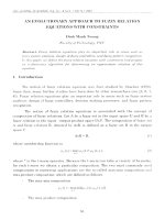
A ssum ing that f { M ) = K is a function satisfying term D irichlet o f Fourier [3]
theorem on period [0, 2”'^ - 1] = [a,b]. In order to develop f(M) into Fourier series, we form a periodic
function g(Fb) having a period either bigger or equal to [b - a" so that
g { F ,) = f { M )
V F, G a ,b \ =
-1
(22 )
Obviously there are m any ways to develop g(Fb) into Fourier series. For each g(Fb) there are
coưesponding Fourier series, therefore there are a number o f Fourier series dem onstrating f(M) = K„
in other words, the circuit function f(M) = Kn with every M is periodical! with period AFb= 2"'“ - 1, in
here A Fb Determine from table 2 .
From dem onsfration above, we realize that circuit function depend on AFb = [0, 2"'" -1], With
circuit functions in proportion to FbỂ [0,
-1] then we have to change F to Fb. so to determine o f
circuit function we need to find the value Fb- From table 2 we have:
Fb = F - 4 . ( n - 3 )
(23)
Now that we can assert that with any variable input n, that is the frenquency divider can
(theoretically) divide to infinite number, then the impulse diagram o f circuit function change
periodically in those periods w hich have sim ilar impulses, that is circuit functions always have form 1
and 2 according to certain A F
To here, we define that circuit function o f frequency divider is change periodically follow a
certain circulate, in other words, circuit function in any form K„.3, K„.4 , K „.5 , K„,6 , ... have same form
apply with same F frequency. From (11) to (18) we can define o f 2 com prehensive forms o f circuit
function o f one frequency divider with output impulse and input as we expect:
K = { Q n - ^ - ^ ( P ) ■ f n i y ) + (P■Qn-^+Qn
(24)
0 i f F = [o, 2"“' - f
With
Ọ=
(25)
\ if
T ~ \ 2"-' - 1
(26)
/„ ừ ) =
>^4
= f { y i )
N.Q. T huong / VN U J o u rn a l o f Science, M athem atics - P hysics 24 (2008) 163-170
169
Com bine form 1 and 2 we realize that circuit function o f frequency divider coưespondence with
any num ber o f input im pulse and num ber o f output impulse expect:
(27)
K .=
(28)
Ô/[(Ổ„-, +
= n
1
Provide: - n is a num ber o f FF participate in frequency divider
- cp is show as function (25)
- f ( y ) is show as function (26)
- K„ Kn-I,... K 4 , K 3 are circuit function coưesponding to different n
4. Determine hazard o f circuit function
From circuit function (28) we can see output state Q o f Fflipflop in negative (Q ) and not
negative Q. Follow [4,5] w hen have same output in negative form and not negative form then a chance
to create hazard
IS
big, so w e need to D eterm inated that circuit s ta y jn one o f static - 0 hazard
(Fig.3a), static-1 hazard x + x (Fig 3b), dynamic hazard XX+ x, (x + x ) x ( Fig.3c,d) or not.
X + XX
XX
a)
c)
(x + x)x
b)
d)
Fig. 3. Basis hazards.
From function (28) w e can build com prehensive circuit o f frequency divider:
From com prehensive circuit w e can construct the residual circuit.
XX
170
N .Q . T h u o n g / V N U J o u rn a l o f Science, M athem atics - P hysics 2 4 (2008) Ỉ 6 3 - Ỉ 7 0
Shown in Fig. 5:
Fig. 5. The residual circuit of frequency divider.
Compare residual circuit o f frequency divider (Fig 5) w ith circuit show ing basic hazards
(Fig.3), w e realize circuits o f basic h azard s where X and X stay in tw o d iffe re n t flat su rfa c e algo rith m
and connected series (Fig. 6 b). It will appear delay in surface X before com e to surface JC, this is cause
o f hazard. On the c o n ừ a ry , with fre q u e n c y divider X and
X
also stay in one su rfa c e algo rith m (Fig.
6 a), they are “equal” on another, so it not delay circuit X to appear hazard. In other word, the
frequency divider showing in (28) is free hazard.
b)
Fig. 6 . Illusfration that frequecy divider is free Hazard.
So because o f function (28) we design frequency divider w ith M atlab softw are without using
Boole algebra. From that we can design frequency divider with any divider factor K using computer,
and free hazard in circuit function.
References
[1] G. Scarbata, Synthese imd Analyse digitaler Schaltungen, Oldenbourg Vcrlag Muenchen Wien (2000).
[2] Nguyen Quy Thuong, Digital Technics, Vietnam University Publishing House, Hanoi (in Vietnamese), (2008) 575
[3] Nguyen Dinh Tri, Ta Van Dinh, Nguyen Ho Quynh, High Mathematics, Education Publishing House, Hanoi (in
Vietnamese), {2004} 415.
[4] John Knight, Cliches and Hazard in Digital Circuits, Elctronics Department, Carleton University (2006).
[5] Erik Meijer, Hazard Algebra for Asynchronous Circuits, POBox 80.089 NL-3508 7B Utrccht The Netherlands
(2006).