DSpace at VNU: Photoelectrical Characteristics of UV Organic Thin-film Transistor Detectors
Bạn đang xem bản rút gọn của tài liệu. Xem và tải ngay bản đầy đủ của tài liệu tại đây (620.41 KB, 8 trang )
VNU Journal of Science: Mathematics – Physics, Vol. 33, No. 2 (2017) 74-81
Photoelectrical Characteristics of UV Organic Thin-film
Transistor Detectors
Dao Thanh Toan*
Faculty of Electrical-Electronic Engineering, University of Transport and Communications,
No.3, Cau Giay, Dong Da, Hanoi, Vietnam
Received 16 March 2017
Revised 25 April 2017; Accepted 20 May 2017
Abstract: In this paper, a pentacene photo organic thin-film transistor (photoOTFT) was
fabricated and characterized. The gate dielectric acted as a sensing layer thanks to it strongly
absorbs UV light. Electrical behaviors of photoOTFT were measured under 365 nm UV
illumination from the gate electrode side. The current in transistor channel was significantly
enhanced by photoelectrons at interface of buffer/gate dielectric. Photosensitivity increased with
the light intensity but decreased with the applied gate voltage. Meanwhile the photoresponsivity
decreased with the light intensity and increased with the applied gate voltage. The transistor
responses well with the pulse of light with many test cycles of light-on and light-off. The best
photosensitivity, photoresponsivity, rising time and falling time parameters of the device were
found to be about 104, 0.12 A/W, and 0.2 s, respectively. The obtained photoelectrical results
suggest that the photoOTFT can be a good candidate for practical uses in low-cost UV
optoelectronics.
Keywords: Pentacene phototransistor, UV sensor, organic electronics, optoelectronics.
1. Introduction
In recent years, electronic components manufacturing from organic materials have been
intensively studied due to their modern applications of low-cost, flexible, large area, lightweight
lighting, and bendable display, which are hard to be realized using conventional inorganic
semiconductors [15]. Evidently, an OLED Television has been succeeded to enter in the market and
the OLED technology is going to occupy in all displays of the modern electronic products. Besides
OLED, photodetection device operating in the ultraviolet (UV) region are increasingly attracting
attention due to a wide variety of potential applications, such as water purification, sterilization,
medicine, fire alarm, ozone sensing, a solar UV radiation monitor , or organic visible light
communication [615]. In recent work [14], we have proposed a new approach to construct a UV
photo pentacence OTFT (organic thin-film transistor) via introducing the photoactive molecules of
_______
Corresponding author. Tel.: 84-979379099.
Email:
/>
74
D.T. Toan / VNU Journal of Science: Mathematics – Physics, Vol. 33, No. 2 (2017) 74-81
75
DPA-CM (6-[4′-(N,N-diphenylamino)phenyl]-3-ethoxycarbonylcoumarin) doped in gate dielectric
polymer of PMMA (poly(methyl methacrylate)). The operation mechanism study realized that the
DPA-CM act as an UV light sensing material that is potential to overcome the limitation of
mismatching the absorption wavelength of the semiconducting material of pentacene with the UV
light wavelength. However, in order to make the transistor device enable for an application in
optoelectronics, the critical photodevice parameters of photosensitivity, response time, and
photoresponsivity of the photoOTFT are necessary to be investigated [5].
In the present work, a photoOFFT with a pentacene semiconductor and a photoactive gate
dielectric is re-fabricated. Then, the photoelectrical characteristics at different applied voltages and
light intensities are measured to estimate the device parameters. The photodevice exhibits a high
photosensitivity or photoresponsivity and fast response characteristic.
2. Experimental methods
(a)
Polystyrene
PMMA/DPA-CM
Pentacene
S/D
S/D
ITO gate
(b)
(c)
(d)
Absorbance
S/D
PhotoOTFT
S/D
1.2
+
induced by
photoelectron
0.8
-
PMMA/DPA-CM
0.4
Pentacene
0.0
300 400 500 600 700 800
Wavelength(nm)
UV
photoactive
molecules
+
+
Gate electrode
Head of UV light source
UV light (=365 nm)
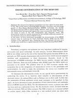
Fig. 1. a, Fabrication process of photoOTFT. S/D stands for source/drain electrodes. Arrow is to indicate
process. b, Absorbance spectra of photoactive dielectric of PMMA/DPA-CM and pentacene measured using
JASCO V-570 spectrometer. c, Illustration of cross-sectional structure and UV light irradiation method. d,
Camera image of fabricated photoOTFT under test.
The photoOTFT was fabricated by employing the previous method [14]. The fabrication process,
device structure and the properties of the main materials are shown in Fig. 1. Firstly, glass substrates
coated with a 150 nm gate electrode layer of indium tin oxide (ITO) were cleaned using
ultrasonication, followed by UV-O3 treatment. PMMA and DPA-CM were dissolved in chloroform at
D.T. Toan / VNU Journal of Science: Mathematics – Physics, Vol. 33, No. 2 (2017) 74-81
76
a concentration 2 wt %. Absorbance spectra of the PMMA/DPA-CM thin-film on quartz are shown in
Fig. 1b. A 260-nm-thick photoactive dielectric layer of the PMMA/DPA-CM was prepared by spincoating and heated on a hot plate at 100 oC for 60 min to remove the residual solvent. Next, a 70-nmthick polystyrene (Aldrich, Mw = 280,000) buffer layer was formed onto the PMMA/DPA-CM layer
by spin-coating of a m-xylene solution (1 wt%) at 1000 rpm for 60 s and dried at 100 oC for 60 min.
The buffer layer here is needed to avoid chemical doping on the semiconducting channel by the
photoelectrons from the photoactive dielectrics. Subsequently, a 50-nm-thick layer of pentacene
(Aldrich, purified by vacuum sublimation twice) was formed on the buffer layer by vacuum deposition
at a deposition rate of 0.02 nm s− 1. Finally, the device was completed by deposition of 50-nm-thick
source-drain electrode of gold at a deposition rate of 0.03 nm s 1 through a designed metal mask to
form the length (L) and width (W) of the channel of 50 and 2000 μm, respectively. The all vacuum
deposition processes were done at a pressure of 2106 Torr.
The thickness of thin film was checked by scratching the film and measuring a height difference
across the scratch with an atomic force microscope (VN-8000, KEYENCE). Electrical measurements
of the photoOTFT were performed using a Keithley 4200 semiconductor characterization system in a
dry nitrogen atmosphere at room temperature. 365 nm UV light generated from an Omron ZUV UV
irradiator was irradiated from a glass substrate side as presented in Figs. 1c and 1d.
3. Results and discussion
Black curves in Fig. 2 present the electrical characteristics of the initial photoOTFT. Regarding
basic transistor device performance, the saturation-region hole mobility () is estimated by fitting the
plot of the square root of drain current (ID) versus gate voltage (VG) with an equation [14]:
ID
W
Ci (VG Vth )2 ,
2L
(1)
where Vth is the threshold voltage. The Vth, on/off current ratio, , and swing factor, estimated from
the transfer characteristics at a drain voltage (VD) of 5 V shown in Fig. 2b, are 3.45 V, 3.48 ×10⁵,
and 0.025 cm2 V-1 s-1, 1.22 V/decade, respectively. The similarity of the initial characteristics to other
organic transistors [1,914] confirming that the fabrication process is proper.
The differences in both transfer and output curves under dark, light, and after light-off shown in
Fig. 2 clearly indicate a UV photo sensing property of the fabricated device. As shown in Fig. 1b, the
absorbance of pentacene at 365 nm is very weak, leading to a photocurrent originating from direct
carrier generation in pentacene is negligible. On other aspect, the absorbance of the PMMA/DPA-CM
is much stronger than that of pentacene in the UV region, resulting in the DPA-CM plays an important
role to construct the UV pentacene photoOTFT. The working principle was detailed in our previous
report [14], here it is briefly explained. When the photoOTFT is irradiated and biased. The chargeseparation state is generated and under the application of a voltage between the gate and drain
electrodes, the charge-separation state is converted into free electrons and holes. Under effect of the
gate electric field, the photogenerated holes move to the ITO gate electrode and the photogenerated
electrons move to the interface of the photoactive/polystyrene buffer layers. The additional electric
field made by the photogenerated electrons further induces additional holes accumulation in the
pentacene transistor channel (see Fig. 1(c)). As the result, the concentration of hole in the channel
becomes larger than that of the device in dark, leading to the increasing the ID as indicated by red
curves in Fig. 2. On the other hand, when the UV light is removed, the PMMA/DPA-CM and buffer
D.T. Toan / VNU Journal of Science: Mathematics – Physics, Vol. 33, No. 2 (2017) 74-81
77
Drain current (A)
Drain current (A)
layer work as a normal gate dielectric layer for field-effect operation and thus hole accumulation in the
transistor channel is inducted by the gate electric field only, leading to decreasing the ID as presented
by black curves in Fig. 2.
10
-6
10
-7
10
-8
10
-9
10
-10
10
-11
10
-12
Light-on
2.45 mW/cm2
(a)
Light-off
Initial dark
-20
-1.2
-1.0 (b)
-0.8
-0.6
-0.4
-0.2
0.0
0
-15
-10
-5
Gate voltage (V)
0
VG= - 18 V, 2.45 mW/cm
2
VG= - 16 V, 2.45 mW/cm
2
VG= - 18 V, dark
VG= - 16 V, dark
-4
-8
-12
Drain voltage (V)
-16
Fig. 2. Transfer (a) and output (b) characteristics of photoOFET under dark and UV light of 2.45 mW/cm 2.
The photosensitivity P of the phototransistor can be estimated by the following equation [5]:
P
I D ,ill I D ,dark
I D ,dark
(2)
where ID,ill and ID,dark are the drain current under light illumination and dark, respectively. Figure 3a
shows the relationship between the P and gate voltage at different light intensities. The P tends to
decrease with applied gate voltage, and almost saturates at UV light intensity higher than 25.60
mW/cm2. This tendency is similar to the experimental data reported by other groups [1214]. The
maximum P is realized at a VG = 2 V as indicated by dotted line in Fig. 3a. Fig. 3b plotted the
maximum P versus light intensity. As can be seen, the large maximum P is obtained to be from 103 to
104 corresponding to increasing light intensity.
The R of the photoOTFT is determined by formula [15]:
R
I D ,ill I D ,dark
Popt A
(3)
where Popt is the incident light intensity, A is the area of the transistor channel, which can be
calculated by W×L. Thus, eq (3) can be converted to be:
D.T. Toan / VNU Journal of Science: Mathematics – Physics, Vol. 33, No. 2 (2017) 74-81
78
R
I D ,ill I D ,dark
Popt W L
(4)
Photosensitivity
Using eq (4) and based on the experimental data, the calculated R is presented in Fig. 4. Unlike P,
the R was found to increase as increasing the applied VG. Also, dependence of the R on the UV light
intensity has been summarized. As shown in Fig. 4b, the R decreased as increasing the light intensity.
At a certain intensity of light, the maximum R (Rmax) was obtained to be in a range of 0.010.1 A/W.
Besides the P and the R, the response time is other important parameter of the photodevice. Figure
5 shows the response time of the photoOTFT at UV light power of 2.45 mW/cm2 recording by a
digital oscilloscope. The VG of 2 V was chosen since at this value, the photodevice can reach the
maximum P as mentioned above. As shown, the repeatable change in the drain current is well
correspondent to the cycle of the light-on and light-off. Utilizing the response behavior, the rising time
(rise) and falling time (fall) were measured to be about 0.2 ms, indicating that the device has a fast
response property in comparison with that in the recent pentacene phototransistor [10].
10
4
10
3
10
2
10
1
VD = - 5 V
2
UV light intensity (mW/cm )
2.54
8.80
25.60
44.30
(a)
0
Pmax
10
-20
10
4
10
3
10
2
10
1
10
0
-15
-10
-5
Gate voltage (V)
0
VD = - 5 V
(b)
0
10
20
30
40
2
Intensity (mW/cm )
50
Fig. 3. Photosensitivity versus gate voltage at various UV light intensities (a) and maximum photosensivity
versus intensity (b) of fabricated photoOTFT at VD of 5 V.
D.T. Toan / VNU Journal of Science: Mathematics – Physics, Vol. 33, No. 2 (2017) 74-81
Photosensitivity (A/W)
10
0
VD = - 5 V
10
-1
10
-2
2
UV light intensity (mW/cm )
2.54
8.80
-4
10
25.60
(a)
44.30
10
-3
10
-5
-20
Rmax (A/W)
10
-15
-10
-5
Gate voltage (V)
0
0
10
-1
10
-2
10
-3
10
-4
10
-5
VD = - 5 V
(b)
0
10
20
30
40
2
Intensity (mW/cm )
50
Fig. 4. (a) Relationship between photoresponsivity and gate voltage at different UV light intensities and (b)
maximum photoresponsivity as function of intensity of fabricated pentacene photoOTFT at VD of 5 V.
-7
Drain current (A)
10
VD = - 5 V, VG = - 2 V
On
On
On
-8
10
-9
10
-10
10
-11
10
0
Off
10
20
30
40
Off
Off
50
60
70
Drain current (%)
Nomalized time (s)
100
90
80
70
60
50
40
30
20
10
0
12
rise=0.2 s
13
14
fall=0.2 s
15
16
Time (s)
17
18
Fig. 5. (Top) Response time characteristics and (Bottom) determinations of rising time and falling time of
pentance photoOTFT.
79
D.T. Toan / VNU Journal of Science: Mathematics – Physics, Vol. 33, No. 2 (2017) 74-81
80
Table 1 presents the summary of device performance of the present pentacene photoOTFT and
relative works reported so far in terms of operating wavelength (), channel area, rise, fall, maximum
P, and maximum R. The R is current device approaches the commercial value and can be comparable
to that in other pentacene based-OTFTs. Significantly, the pentacene photoOTFT shows advancement
with respect to the rise, fall, P. This is due to the fact that the photoOTFT was designed and made
using a different approach, where the gate dielectric works as a UV sensing layer.
Table 1. Summary of device performance of current photoOTFT and relative photodevices.
(s)
(s)
N/A
N/A
364
90500
365
UV sensor
(nm)
LW
(m m)
Inorganic SiC
210-380
Pentacene
OTFT
Pentacene
OTFT
Pentacene
OTFT
Pentacene
OTFT
Pentacene
OTFT
P
R
(A/W)
Year, Ref
N/A
N/A
0.13
Industry, Ref. 6
N/A
N/A
1.010
N/A
2006, Ref. 9
504000
60
60
1.010
0.015
2009, Ref. 10
365
1004000
N/A
N/A
1.210
0.07
2012, Ref. 12
350
10017200
N/A
N/A
1.010
0.08
2013, Ref. 13
365
502000
0.2
0.2
1.010
0.12
Current work
rise
fall
1
4
4
4
4
4. Conclusions
In conclusion, an UV pentacene photoOTFT with a sensing layer of gate dielectric has been
fabricated and characterized. Electrical behaviors of phototransistor were investigated at 365 nm UV
irradiation from the gate electrode side. The enhancement of the photocurrent in transistor channel
resulted from the photoelectrons at the buffer/gate dielectric interface. Photosensitivity was found to
increase with the light intensity and decrease with the VG. On contrast, the photoresponsivity was
observed to decrease with the light power and increase with the VG. The pentecene transistor rapidly
responded with the light-on and light-off. The highest photosensitivity, largest photoresponsivity,
fastest rising/falling time of the phototransistors were recorded to be 10 4, 0.12 A/W, and 0.2 s,
respectively. Such photoelectrical data indicate that the fabricated photoOTFT is highly potential for
practical low-cost UV optoelectronic circuits.
Acknowledgements
Author would like to thank the International Information Science Foundation, 2016, Tokyo, Japan
(grant no. 2016.1.3.126) and Prof. H. Sakai, JAIST, Japan for supporting facilities of semiconductor
component manufacturing.
D.T. Toan / VNU Journal of Science: Mathematics – Physics, Vol. 33, No. 2 (2017) 74-81
81
References
[1] R. Liguori , W.C. Sheets, A. Facchetti, A. Rubino, Light- and bias-induced effects in pentacene-based thin film
phototransistors with a photocurable polymer dielectric, Organic Electronics, 28 (2016) 147.
[2] N. N. Dinh, D. N. Chung, T. T. Thao, T. T. Chung Thuy, L. H. Chi, T. Vo-Van, Enhancement of performance of
organic light emitting diodes by using Ti- and Mo-oxide nano hybrid layers, Mater. Sci. Appl., 4 (2013) 275.
[3] N. N. Dinh, T. T. Thao, D. N. Chung, V.-V. Truong, Characterization of organic solar cells made from hybrid
photoactive materials of P3HT:PCBM/nc-TiO2, VNU Journal of Mathematics – Physics, 30 (2014) 8.
[4] M.H. Hoang, T.T. Dao, N.T.T. Trang, P.H.N. Nguyen, T.T. Ngo, Synthesis of gold nanoparticles capped with
quaterthiophene for transistor and resistor memory devices, Journal of Chemistry, 2016 (2016) 8 pages.
[5] Y. Wakayama, R. Hayakawa, H.-S. Seo, Recent progress in photoactive organic field-effect transistors, Sci.
Technol. Adv. Mater. 15, (2014) 024202.
[6] accessed 16 March 16, 2017.
[7] S.R. Forrest, Active optoelectronics using thin-film organic semiconductors, IEEE J. Select. Topics Quantum
Electron. 6 (2000) 1072.
[8] T.D. Anthopoulos, Electro-optical circuits based on light-sensing ambipolar organic field-effect transistors, App.
Phys. Lett. 91 (2007) 113513.
[9] J.-M. Choi, J. Lee, D. K. Hwang, J. H. Kim, S. Im, Comparative study of the photoresponse from tetracene-based
and pentacene-based thin-film transistors, Appl. Phys. Lett. 88 (2006) 043508.
[10] B. Lucas, A. El Amrani, M. Chakaroun, B. Ratier, R. Antony, A. Moliton, Ultraviolet light effect on electrical
properties of a flexible organic thin film transistor, Thin Solid Films, 517 (2009) 6280.
[11] El Amrani, B. Lucas, F. Hijazi, A. Skaiky, T. Trigaud, M. Aldissi, Transparent pentacene-based photoconductor:
high photoconductivity effect, Eur.Phys. J. Appl. Phys. 51 (2010) 33207.
[12] A. El Amrani, B. Lucas, B. Ratier, The effect of the active layer thickness on the performance of pentacene-based
phototransistors, Synthetic Metals, 161 (2012) 2566.
[13] D. Yang, L. Zhang, S. Y. Yang, B. S. Zou, Influence of the dielectric PMMA layer on the detectivity of
pentacene-based photodetector ưith field-effect transistor configuration in visible region, IEEE Photonics Journal,
5 (2013) 6801709.
[14] T. T. Dao, T. Matsushima, M. Murakami, K. Ohkubo, S. Fukuzumi, and H.Murata, Enhancement of ultraviolet
light responsivity of a pentacene photoOTFT by introducing photoactive molecules into a gate dielectric, Jpn. J.
Appl.Phys., 53 (2014) 02BB03.
[15] S.-H. Yuan, Z. Pei, H.-C. Lai, C.-H. Chen, P.-W. Li, Y.-J. Chan, Au nanoparticle light scattering enhanced
responsivity in pentacene phototransistor for deep-UV light detection, IEEE Electron Device Letters, 36 (2015)
1186.