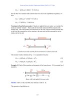
3 FET fundamentals
Bạn đang xem bản rút gọn của tài liệu. Xem và tải ngay bản đầy đủ của tài liệu tại đây (7.97 MB, 214 trang )
FET Basics
• Fundamentals: definition, structure,
operations and characteristics
• Biasing of FET
• Modeling of FET and small signal
analysis
• DC and AC load line analysis
• FET amplifier configurations and
design
• FET applications
Introduction of FET
An FET (field-effect transistor) operates on either electrons or holes flow. Hence it
is a unipolar transistor, i.e. single-type of current carriers.
Whereas a BJT is a current controlled device, a FET is a voltage controlled device.
It has an extremely high input resistance (in the order of 107 to 1012).
It requires virtually no input (gate) current IG = 0 A.
Also used as amplifier and logic switches
It is preferred over BJT as the input stage of a multi-stage amplifier.
FETs generate low noise and are more temperature stable than BJTs. (It does not
depend on electron-hole pair for current conduction.)
Therefore they are more suitable for amplification of very small signals.
As there is no minority carrier storage time (no p-n junction recovery time) for FETs,
they are widely used (very popular indeed) in switching applications.
FET analogy, bias, and currents
The source of water
pressure can be
likened to the applied
voltage from drain to
source that will
establish a flow of
water (electrons) from
the spigot (source).
The “gate" through an
applied signal
(potential), controls
the flow of water
(charge) to the "drain”
The drain
and source terminals
are at opposite ends or
the n-channel as
introduced in Figure
3
Introduction of FET
There are two major types of FETs.
(a) Junction FET (JFET), and
(b) Metal Oxide Semiconductor (or silicon) FET (MOSFET)
(i) Depletion-type MOSFET (D-MOSFET)
(ii) Enhancement-type MOSFET (E-MOSFET), and
(iii) Vertical MOSFET (VMOS).
Each type can be further classified into n-channel or p-channel MOSFETs.
Major Types of FETs
FET
JFET
p-channel
n-channel
p-channel
MOSFET
Depletion Type
n-channel
p-channel
Enhancement Type
Conventional
Structure
n-channel
VMOS
p-channel
n-channel
Metal Oxide Silicon FET (MOSFET)
There are two basic types of MOSFET
- Depletion-type MOSFET (D-MOSFET)
- Enhancement-type MOSFET (E-MOSFET)
The gate terminal of a MOSFET is insulated from its channel
region by the Silicon Oxide (SiO2) layer.
MOSFET is also called an Insulated-Gate FET (IGFET).
FET Properties
• Advantages:
– High input impedance (M)
(Linear AC amplifier system)
– Temperature stable than BJT
– Smaller than BJT
– Can be fabricated with fewer processing
– BJT is bipolar – conduction both hole and electron
– FET is unipolar – uses only one type of current carrier
– Less noise compare to BJT
– Usually use as logic switch
• Disadvantages
– Easy to damage compare to BJT
7
JFET
8
JFET Fundamentals
9
Junction FET
• There are 2 types of JFET
– n-channel JFET
– p-channel JFET
• Three Terminal
– Drain – D
– Gate -G
– Source – S
n-channel JFET
p-channel JFET
Water analogy for the JFET
control mechanism
N-channel JFET
• N channel JFET:
– Major structure is n-type material (channel) between
embedded p-type material to form 2 p-n junction.
– In the normal operation of an n-channel device, the Drain
(D) is positive with respect to the Source (S). Current flows
into the Drain (D), through the channel, and out of the Sour
ce (S)
– Because the resistance of the channel depends on the
gate-to-source voltage (VGS), the drain current (ID) is control
led by that voltage
N-channel JFET
• Current can flow initially because plenty of electrons are
available in the channel.
• Gate : Apply negative voltage to increase the depletion
width, so as to reduce the current. When the gate voltag
e is negative enough, current will stop.
• Hence, this is a depletion device.
N-channel JFET
• Pinch off in JFET (that bop)
P-channel JFET
• P channel JFET:
– Major structure is p-type material (channel) between
embedded n-type material to form 2 p-n junction.
– Current flow : from Source (S) to Drain (D)
– Holes injected to Source (S) through p-type channel
and flowed to Drain (D)
JFET Characteristic Curve (N-Channel)
• To start, suppose VGS=0
• Then, when VDS is increased, ID increases. Therefore, ID is
proportional to VDS for small values of VDS
• For larger value of VDS, as VDS increases, the depletion layer
become wider, causing the resistance of channel increases.
• After the pinch-off voltage (Vp) is reached, the ID becomes
nearly constant (called as ID maximum, IDSS-Drain to Source c
urrent with Gate Shorted)
ID versus VDS for VGS = 0 V.
JFET for VGS = 0 V and 0
Channel
becomes
narrower as
VDS is
increased
Pinch-off (VGS = 0 V, VDS = VP).
Application of a negative voltage to the
gate of a JFET.
JFET Characteristic Curve (N-Channel)
•
For negative values of VGS, the gate-to-channel junction
is reverse biased even with VDS=0
•
Thus, the initial channel resistance is higher (in which
the initial slope of the curves is smaller for values of
VGS closer to the pinch-off voltage (VP)
•
The resistance value is under the control of V GS
•
If VGS is less than pinch-off voltage, the resistance
becomes an open-circuit ;therefore the device is in
cutoff (VGS=VGS(off) )
•
The region where ID constant – The saturation/pinch-off
region
The region where ID depends on VDS is called the
linear/triode/ohmic region
•
n-Channel JFET characteristics curve
n-Channel JFET characteristics curve
n-Channel JFET characteristics curve
with IDSS = 8 mA and VP = -4 V.
JFET Characteristic Curve
JFET Characteristic Curve (P-Channel)
• Operation is almost the same as n-channel FETs.
• Voltage polarity and current direction reversed.
• BUT… for p-channel devices,
– The carriers are holes (not electrons). So, mobility is
lower and minority carrier lifetime shorter.
– Consequence: p-channel devices are usually POORER!
• Higher threshold voltage, higher resistance, and lower current capability.
p-Channel JFET
p-Channel JFET characteristics with IDSS = 6 mA
and VP = +6 V.